Note: Descriptions are shown in the official language in which they were submitted.
78~
The purpose of the disclosed serial data bus is to
allow multiple microprocessors to easily communicate with each
other over a common pair of wires using a scheme similar to a
telephone party line. The invention relates to data
communications links between members of a distributed
processing multiplex system in ~ vehicle such as an
automobile. The serial data bus and interface integrated
circuit developed and disclosed herein is capable of
supporting many types of communication protocols.
Description of the Prior Art
Data communications between microprocessors or
microcomputers need to communicate with each other in many
applications.
Local area networks (LAN) link such microprocessors
or microcomputers, allowing one of the microcomputers to seize
control of the serial data channel commonly linked to all
other microprocessors on the LAN and transmit data to any
other unit. The protocols, controllers and software needed in
a LAN are very complex, especially in large systems.
An automotive environment is a smaller application
and, thus, does not require the complex performance
capabilities available in a LAN.
Digital data buses have been designed to handle the
above-described data communications link in a small area.
Such a system is described in SAE Paper No. 840317, by Ronald
L. Mitchell entitled "A Small Area Network for Cars". Also
descriptive of such a digital data bus is U.S. Patent No.
4,429,384 to Kaplinsky entitled "Communication System Having
An Information Bus And Circuits Therefor".
Also descriptive of developments in this field is SAE
Paper No. 860390 by Frederick H. Phail and David J. Arnett
entitled "In Vehicle Networking - Serial Communications
Requirements and Directions".
The subject invention differs from the art noted
above by use of a constant speed, the lack of use of an
acknowledgement bit and the lack of requirements for a tight
link between the transmitting station and the receiving
rn/J~
~ v~
` ~'78~2
stations. Also Import~nt In the subject inventlon i5 the communlcation link between
the message transmitter and recelver.
Generally, the ~ollowing U.S. patents discuss collision detection in data
communications systems: U.S. Patent No. 4,281,380 of DeMesa 111 et al. entitled
"Bus Collision Avoidance System For Distributed Network Data Processing
Communications System" dated July 28, 1981; U.S. Patent No. 4,409,592 of V. Bruce
Hunt entitled "Multipoint Packet Data Communication System Usin~ Random
Access And Collision Detection Technigues" dated October 11, 1983; U.S. Patent
No. 4,434,421 of Baker et al. entitled "Method For Digital Data Transmission With
Bit-Echoed Arbitration" dated February 28, 1984; U.S. Patent No. 4,470,110 of
Chiarottino et al. entitled "System For Distributed Priority Arbitration Among
Several Processing Units Competing For Access To A Common Data Channel" dated
September 4, 1984; and U.S. Patent No. 4,472,712 of Ault et al. entitled "Multipoint
Data Communication System With Local Arbitration" dated September 18, 1984.
The U.S. Patent No. 4,434,421 patent to Baker et al. deals with a method
to reduce the number o~ collisions. This is done by reducing the number of slavestations attempting bus access until there is one master and one slave station in
communication. This differs from the subject invention in that a broadcast method
is employed whereby several users can receive the same message.
The U.S. Patent No. 49470,110 to Chiarottino et al. discloses a system to
exchange messages including an interface. In addition, the '110 patent assigns apriority to an address bit of a particular logicaJ level.
Also of interest is an article in an IEEE publication "Automotive
Applications of Microprocesors," 1984; Paper No. CH2072-7/84/0000-0083 entitled
"A Data Link For Agricultural And Off Highway Communications" by Boyd Nichols,
Vijay Dharia and Kanaparty Rao.
Of paramount importance in the subject invention is the inclusion of the
capability to communicate with a serial communication interface (SCI) port, a serial
peripheral interface (SPI) port and a buffered serial peripheral interface (BSPI) port.
7~7~ `
SUMMARY OF THE INVENTION
The purpose of the serial data bus system disclosed
herein, also known as Chrysler Collision Detection (C2D) bus,
is to allow multiple microprocessors to easily communicate
with each other over a common pair of wires or bus using a
scheme similar to a telephone party line. All microprocessors
connected to the bus are able to receive all messages
transmitted on the bus. Any microprocessor with a message to
transmit on the bus waits until any current user is finished
before attempting to use it.
Whenever the bus is available, its use is allocated
on first-come first-serve basis. That is, whichever
microprocessor begins transmitting its message on the bus,
after any previous message finishes, gets the use of the bus.
If, however, multiple microprocessors attempt to begin
transmitting their messages on the bus at exactly the same
time, then the message with the highest priority wins the use
of the bus. All messages have unique message priority values
and each message is transmitted by only one microprocessor.
The invention disclosed herein is further summarized
in applicant's U.S. Patents Nos. 4,706,082 and 4,719,458,
issued November 10, 1987 and January 12, 1988, respectively.
Also relevant is SAE Information Report entitled
"J1567 Collision Detection Serial Data Communications
Multiplex Bus" to be presented to the SAE Multiplexing
Committee by Frederick O.R. Miesterfeld on May 23, 1986.
Attention is invited to the above-described patents
for further explanation of the summaries of some of the basics
of the invention described in the subject application.
It i5 an object of the subject invention to provide
an SCI port, an SPI port and a buffered SPI port as part of
the serial data interface integrated circuit described herein.
This allows communication with any device configured with any
rn/
~27~3~372
~one ~f these thrce ports all on the s~me bus. The IncJusion of the ports augments
the simplification of the serial data communication described in the
patents identified above.
DESCRIPTION OF THE DRAWINGS
Other objects, ~eatures and advantages of the present invention will
become more fully apparent from the following detailed description oi the preferred
embodiment, the appended claims and in the accompanying drawings In which:
Fig. 1 is a block diagram showing a serial data bus network;
Fig. 2 illustrates the hardware for the serial data bus described herein;
Fig. 3 is a continuation of the hardware drawing for the serial data bus;
Fig. 4 is a block diagram of the bus interface integrated circuit (IC);
Fig. S is a timing diagram showing an example of the collision detection
on the bus interface IC during arbitration;
Fig. 6 is a gate diagram of the arbitration detector 42;
Fig. 7 is a gate diagram of the collision de$ector 44;
Fig. 8 is a gate dlagram of the start bit detector 200;
Fig. 9 is a ~ate diagram of a clock diYider 201;
Fig. 10 is a gate diagram of a word counter 202;
Fig. I l is a gate diagram of a flip-~lop 203;
Fig. 12 is a gate diagram of framing error detector 204;
Fig. 13 is a gate diagram of idle counter 206;
Fig. 14 is a gate diagram of idle flip-flop 207;
Fig. lS is a gate diagram of digital filter 210;
Fig. 16 is a gate diagram of mode select 301;
Fig. 17 is a gate diagram of SCK selector 302;
Fig. 18 is a gate diagram of SCK counter 303;
Fig. 19 is a gate diagram of a 16-bit buffer and bit reverser 304;
Fig. 20 is a gate diagram of a 2 or I byte receive 305;
Fig. 21 is a gate diagram of a 2 byte counter 306;
Fig. 22 is a gate diagram of a start/stop bit generator and SPI data path
307;
Fig. 23 is a gate diagram of SPI clock generator 308;
1~88'a~2
Figure 24 is a gate diagram of SPI transmit scheduler
and controller 309;
Figure 25 is a gate diagram of test mode detector
401;
Figure 26 is a gate diagram of reset circuit 402;
Figure 27 is a gate diagram of break generator 403;
and
Figure 28 is a gate diagram of an over range latch.
DETAILED DESCRIPTION OF THE PREFERRED EMBQDIMENT
This application is one of three filed by the
applicant on the same day, ~ay 21, 1987, and having related
specifications and drawings. The other cases are commonly
owned with the same inventors and are Serial No. 537,661,
entitled "Method for buffered Serial Peripheral Interface
(SPI) in a Serial Data Bus" and Serial No~ 537,662, entitled
"Method For Serial Peripheral Interface In A Serial Data Bus".
Further documents of relevance include U.S. Patent
No. 4,429,384 issued to Kaplinsky and entitled "Communication
System Having An Information Bus And Circuits Therefor"; SAE
Technical Paper No. 830536 entitled "Serial Bus Structures For
Automotive Applications" by Anthony J. Bozzini and Alex
Goldberger dated February 28, 1983; SAE Paper No. 840317 by
Ronald L. Mitchell entitled "A Small Area Network for Cars";
SAE Paper No. 860390 by Frederick H. Phail and David J. Arnett
entitled "In-Vehicle Networking - Serial Data Communication
Requirements And Directions"; and SAE Paper No. 860389 by
Frederick O.R. Miesterfeld entitled "Chrysler Collision
rn~c
~27~
5a
Detection (C2D) A Revolutionary Vehicle Network'~.
Attention is invited to U.S. Patents Nos. 4,706,082
and 4,719,458 and the concurrently filed copending Canadian
patent applications identified above, for a more complete
description of some of the hardware disclosed in Figure 1,
Figure 2, Figure 3 and Figure 4.
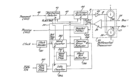
The interaction between the arbitration detector 42,
collision detector 44, word counter 202, word flip-flop 203,
start bit detector 200, framing error detector 204, idle
counter 206, idle flip-flop 207, clock divider 201, digital
filter 210, bus driver made up of OR gate 62 and NAND gate 63,
along with bus receiver 30 in conjunction with current source
34 and current sink 36 as connected to the bus 26.
An understanding of the above-listed blocks is
necessary for understanding the improvements outlined in the
subject application. Attention is, therefore, invited to U.S.
patents Nos. 4,706,082 and 4,719,458 and the explanations
included therein and the drawings.
rn/
8~37~ j
~ eferring now to Fig. 1, Fig. 2, Fig. 3 and Fig. 4, the hardware for the
serial data bus is shown.
SCl MODE O~ OPERATION5
The circuit shown in Fig. 1, Fig. 2, Fi~. 3 and Fi~. 4, used to obtain SCI
operation are used for the other modes of operation and are basic to the entire
interIace IC.
. When the start bit detector 200 senses a valid start bit, it causes the
word counter 202 to synchronize itself to the timing of the received data word. The
word counter 202 is used to generate pulses, one for the collision detector 44 and
another for the word flip-flop 203. At 1/4 bit time, the word flip-flop 203 clocks
the arbitration detector 42. The word counter 202 triggers the framin~ error
detector 204 at the stop bit time. If the stop bit is not detected, the idle counter
206 is extended by the framin~ error detector 204 until 10 idle periods in a strin~
are received.
The collision detector 44 samples the transrnitted input and received
output. It is the function of the collision detector 44 to block transrnission that
could interrupt bus 26 operations. II two or more user microprocessors 22 want to
transmit at about the same time, the arbitration detector 42 will allow transmission
on a ~irst-come first-serve basis. If the user microprocessors 22 both try to
transmit in synchronism, that is within an arbitration window of time, the collision
detector 44 will permit only the one with the highest priority to continue I
transmittin~. ¦
When a user microprocessor 22 is connected to the bus 26 and is ready
for transmission, it shall use the following procedure. First, the user microprocessor
looks at thè IDLE line and waits until it goes to a logical zero, indicatin~ that the
bus 26 is idle. Then the user microprocessor 22 tries to transmit an 8-bit ID word
associated with the data to be transmitted. If the user microprocessor 22 started
transmitting first or has the highest priority ID, the collision detector 44 and I
arbitration detector 42 will permit transmission. The user microprocessor 22
confirms transmission by reading the received ID word by comparing it with the ID
it wanted to transrnit. If there is a confirmation that the same ID was transmitted,
-6-
,;
~ 88
then the data can b~ ~ran5mitted. 1~ not, then the user rnicroprocessor needs tocheck to see lf the recei~ed ID and data 15 needed for Its own use.
It is important to realize that data collision may resu~t due to ou~side
interference or a request for arbitration when long data strings are transmitted.
The user microprocessor 22 that is transmitting data can compare the transmitteddata with the received data Ior this type of collision. Appropriate action should
then be taken by the user microprocessor 22.
The function of the idle counter 206 and idle flip-flop 207 is to detect
when the bus 26 is in the idle condition. This is accomplished by sensing a received
stop bit. A deJay is then imposed for a short idle period of ten bit times. The IDLE
output is then set to a logiaJ zero. The IDLE line is set to a logical one by
receiYing a start bit. This signal is also used to terminate transmission not allowing
transmission during a received signal message. The idle counter 206 and idle fli~
flop 207 also supply a reset signal to the collision detector 44 at the beginning of an
idle period.
A request for arbitration can be generated by a module that needs to
interrupt transmission of a long data string. The way this can be accomplished is by
~orcing the IDL input to a logical zero; this forces a data collision after
transmitting the start bit of the fifth byte, and the transmitting user microprocessor
22 is required to detect this and stop transmitting. It is, however, allowed to again
arbitrate for the bus 26, but the interrupting module may not cause a second data
collision if it loses arbitration.
In the SCI mode, the bus interface 24 supports a typical full duplex
asynchronous serial communications interface for transfer of data bytes to and from
a user microprocessor 22.
In addition to the asynchronous data interfaces, the user microprocessor
must also have an interface to the bus interface IC 24 for the IDLE line and forcontrol purposes.
In the SCI mode, when a user rnicroprocessor 22 wants to send a message
on the bus 26, it sends and receives each byte one at a time and monitors its
pro~ress. As the bits of a byte are sent from the transmit line of the SCI port of the
~` ~ d
user microprocessor 22, they are passed throu~h the bus lnter~ace IC 24 and onto the
bus 26.
Simultaneously, the bits on the bus 26 are detected by the bus interface
IC 24 and passed to the receive line of the user microprocessors 22 SCI port. The
user microprocessor 22 compares the received/reflected byte to the last transmitted
byte and, if they are equal, the user microprocessor 22 knows that the last byte was
transmitted successfuJly and can go on to process the remaining bytes. When the
messages are transmitted on the bus 26 by other user microprocessors 22, the businterface IC 24 receives then one byte at a time through the receive line of its SCI
port.
The user microprocessor 22 must monitor the IDLE line in order to
determine when the last byte of a message has been received, when the next
received byte will be the ~irst message and when it is arbitration time.
SPl MODE OF OPERATION
In this mode, the word counter 202 generates the $iming signals to drive
the SCK counter 303 in conjunction with the SCK selector 302 and the start bit
detector 200. The user microprocessor 22 becomes a slave to the bus interface IC24. When the user microprocessor 22 needs to transmit a word, it loads that wordinto its buffer register and watches for the IDLE pin of the bus interface 24 to 8
to a logical zero signifying that the bus 26 is idle.
The user microprocessor then pulses the CONTROL pin of the bus ¦
interface IC 24. This sets an XMIT eNABLE register within the scheduler and
controller 309 to transmit. The bus interface IC 24 will then generate a start pulse
and supply the user microprocessor 22 with 8 SCK shift pulses in synchronizationwith the start pulse. If a collision is detected on the message ID byte by the user
microprocessor 22, the user microprocessor 22 stops transmitting immediately andstarts receiving. If no collision is detected, this means that the user microprocessor
22 has won arbitration and it, therefore, completes data transmission.
Synchronizer Jogic works with the SPI clock generator 308 and produces
synchronized shift clock pulses for both receiving and transmitting of data. j
However, it does not output shift pulses for start and stop bits. A very accurate
- ~
clock is requ~red here to synchronlze an established data tran5mission/receptlonrate.
In the 5PI mode, the bus interface IC 24 supports the SPI type of
interface facilities available on some model microprocessors.
With the generalJy avaiJabJe SPI suppor~, two microprocessor ~amiJy
devices, one a master and the other a sJave, interchange at high speed, two bytes of
data, c~ne bit at a time, with data synchronization controJled by a clock signalsupplied by the master device.
With the bus interface IC 24 in the transmit mode, one byte of data is,
one bit at a time, simultaneousJy transferred to the bus interface IC 24, $ransmitted
onto the bus 26, while a received refJected bit is received from the bus 26 and
transferred back to the user microprocessor 22. At the end of a one-byte transmit
cycJe, the user microprocessor 22 has, in its SPI data register, the byte that reflects
the transmission of the byte that was in its SPI data register when the user
microprocessor ~2 pulled the CONTROL line low to request the beginning of the
transmission cycJe.
When the bus interface IC 24 begins to receive a byte of data ~rom the
bus 26 before $he user microprocessor 22 pulls the CONTROL line low, the bus
interface IC 24 pulls the CONTROL line low and starts generating the SCK cJock
signaJ. As each data bit is received, it is clocked out of the bus interface IC 24 into
the user microprocessor 22. Any data in the user microprocessor's SPI data register
before the SCK signaJ starts is transferred out of the data register to nowhere as
the received data is transferred into the SPI data register.
In some cases, it may be usefuJ to connect the CONTROL line of the bus
interface IC 24 to the SS line of the user microprocessor SPI port as an aJternative
to other ways of setting the SS low.
There is a slight time deJay between the transfer of the bit from the user
microprocessor 22 to the bus interface IC 24 on the rising edge of an SCK cycJe and
the transfer of the bit from the bus interface IC to the user microprocessor on the
faJling edge of the same SCK cycle.
Data transfers between the user microprocessor 22 and the bus interface
IC 24 occur at the bus transfer speed, 7,812.5 bits per second. ¦ !
2'i~
SPI mode differs from the 5CI rnode mainly because o~ the dif~erences
between SPI types o~ interfaces ~nd S.CI types of interfaces. In the 5PI mod~, the
user microprocessor 22 does not have access to the start and stop bits transmitted
on the bus 26. In the SPI mode, the user microprocessor must reverse the bit order
of transmitted and received bytes.
SPI mode is similar to the SCI mode in that the user microprocessor 22
sends or receives data to and from the bus interface IC 24 one byte at a time. When
transmitting a message, each bit of a transmitted byte is simultaneously transmitted
onto the bus while the reflected bit is received from the bus 26.
In SPI terms, the user microprocessor 22 operates in the slave mode and
the bus interface IC 24 operates as the master. I
In functional terms, the user microprocessor 22 in the bus interface IC ~,
24 are on somewhat equaJ terms with the bus interface IC 24 being more equal than
the user microprocessor 22 as both can initiate a data transfer. The user
microprocessor 22 can request the transmission of a byte by the bus interface IC 24
by pullin~ the CONTROL line low, but it has to do so before the bus interface IC 24
be~ins receiving data from the bus.
As a slave to the bus interface 24, the user microprocessor 22 must be
able to handle the use of the SPI port at any time by the bus interface IC 24.
Data is transmitted on the bus 26 in an asynchronous fashion with a start
bit, eight data bits and a stop bit. The order of data bits is the least significant bit
(LSB), bits 1, 2, 3, 4, 5, 6 and MSB. In an SPI transfer, a user microprocessor 22
normally transfers the MSB first and the LSB last, just the opposite of the bus
transmission.
In order to use SPI mode, the user microprocessor 22 must reverse the
bit order of all transmitted and received bytes. (This problem does not occur in the
buffered SPI mode explained below.)
BUFFERED SPI MODE OF OPERATION
The buffered SPI mode required additional circuits to that used in the
SCI and SPI modes. A 16-bit buffer and bit reverser 30~ is provided for both
receiving and transmitting data. A control flip-flop is used to determine whether
_ 10-
~`\` ~ l
~ 8~
the buffer 304 ls connect~d to the user microprocessor 22 or to th~ bus transmitcircuitry.
When powered up the control ~lip-flop Is connected to the user
microprocessor 22. The user microprocessor 22 is the master and the bus interface
IC 24 is a slave peripheral. The user microprocessor 22 can be connected to other
peripheral ICs and the bus interface IC 24 will be selected by the CS pin (chip select
not pin). When the user microprocessor 22 wants to transmit it selects the bus
interface IC 24 by outputting a zero to the CS pin and then watches the
CONTROL pin. When the control pin goes to a logical one signifying that the
buffer register 304 is full of received data and can be read by the user
microprocessor 22 the user microprocessor 22 then supplies the 16 shift pulses and
reads the data at the same time it loads the SPI bufIer in block 304 with the ID and
data it wants to transmit.
The user microprocessor 22 then pulses the CONTROL pin and the data
will be transmitted at the proper time. If the microcomputer just wants to read it
just reads by supplying the shift clocks and does not pulse the CONTROL pin. Thebus interface IC 24 contains the circuitry to hold the received data in the buffer
register and ignore receiYing new data until after the old data has been read. This
ensures that the transmitted data can be tested to be sure that it won arbitration; if ¦
not it will need to be re-transmitted.
In the buffered SPI mode the bus interface IC 24 uses an internal 16-bit
shift register called a 16-bit buffer and bit reverser 304 to buffer two bytes of data
between the user microprocessor 22 and the bus 26 while supporting the use of the
typical SPI type of interface for the transfer of data between the user ¦
microprocessor 22 and the bus interface IC 24. ¦
The two byte buffer separates the user microprocessor 22 from the
operation of the bus 26. This allows the user microprocessor 22 to concentrate on
other higher priority tasks and to have multiple devices on its SPI bus.
The user microprocessor 22 loads the two-byte buIfer in the bus ¦
interface IC 24 at high speed using an SPI interface and signals the bus interface IC
24 to transmit the data in the buffer. ¦ i
-Il-
.
-\`
The bus Interlace IC 24 at bus speed, ~ttempts to transmit the buffercd
data to the bus 26. During thls attempt to transmitl the bus Interface IC 24
receives two bytes ol reflected data back from the bus 26, s~ores them in the buffer
and locks the buffer from receiving further data from the bus 26 until the received
data is unloaded by the user microprocessor.
Later, the user microprocessor 22, again using the high speed SPI
trans~er technique, unloads the received bytes and simultaneously loads the nextbytes to be transmitted.
While it is transmitting and receiving two bytes of data to and from the
bus, the bus interface IC 24 is not transferring data to and from the microprocessor
22 and, in fact, does not need to be chip selected by the user microprocessor 22durin~ this time.
The user microprocessor uses the IDLE and CONTROL line to sense the
status of the bus interface IC 24 and to control its operation.
The principle differences between the buffered SPI and the unbuffered
SPI rnode are the use of a two-byte internal buffer, that the user microprocessor 22
operates in master mode instead of slave mode and, the separate rather than
combined steps of transferrin~ data between the bus interface IC 24 buffer and the
user microprocessor 22, and transmitting/receiving data to/from the bus 26.
Referring now to Fig. 2 and Fig. 3, the hardware of the bus interface IC
will be described.
The mode select block 301 is composed mostly of data multiplexers and
gates well known to those who design ICs. The function of the mode select block
301 is to control data and the shift clock (SCK) signal flow into and out of the bus
interface IC 24. The MODE and CS (active low) inputs determine which one of the
three modes the bus interface IC is in.
If the MODE and CS inputs are a logical one value, the bus interface IC
24 is in the SCI mode. Here data flows from the XMIT (transmit) pin and is gateddirectly to an output of mode select block 301 to the arbitration detector 42. In
addition, the data to be sent to the received data (REC) pin comes into the block
301 from the digital filter 210.
-12-
.
. . 1.1
7887~
If the MODE Input Is at a 3O~ical one 5tate and the CS input Is at a
logical zero, then the bus interface IC 24 is in the SPI mode. In the SPI mode, data
is input to the bus interface IC 24 in a synchronous fashion in which the bus j
interface IC 24 is the master. When the user microprocessor 22 is transmitting, the
SCK output produces rising and falling ed~es which will induce the user
microprocessor 22 to output data on the risinK edge and will latch data into itself on
the f al ling edge.
The SCK pulses for the SCK pin come into the block 301 from the SPI
clock generator 308. Data that comes in from the XMIT pin is sent out to the
start/stop bit generator and SPI data path 307 for start and stop bit generation.
Data from the start/stop bit generator 307 comes back into the mode seJect block301 and is then sent out on an output line to arbitration detector 42. Data for the
REC pin from the mode select bJock 301, while in the SPI mode, comes from the
digital filter 210.
If the MODE pin is at a logicaJ zero state, the bus interface IC 24 is in
the buffered SPI mode. In this mode, the CS input acts as a true chip select.
If the CS is a Jogical zero, the REC pin will be in the active or driving
state. If the CS input is at a logical one, the REC pin will be in a hi8h impedance
state, and any SCK pulses entering the bus interface IC 24 will be blocked.
While in the buffered SPI mode, the user microprocessor 22 is the
master, which means that the user microprocessor 22 must supply ~he SCK pulses.
The user microprocessor 22 selects the chip or bus interface IC 24 via the CS input
and produces 16 SCK pulses, the data associated with these pulses will be put into a 1 ; -
16 bit buffer and bit reverser 304 via mode select 301. The 16-bit buffer and bit
reverser 304 is clocked from SCK selector 302.
Data from the XMIT pin flows from that pin out of the mode select block
301 and into the 16-bit buffer and bit reverser 304. While the buffer is being
clocked, data intended for the receive pin REC is sent from the buffer Yia the 2 or 1
byte receive block 305.
The mode select block 301 also supports a test mode facility. This is
signal to the block 301 from the test mode detector 401 in combination with the
reset circuit 402. This signal will pass the data from the over range latch 61 to the
,
788~2
REC pin. REC pin on the mode ~elect block 301. The test mode detector 401
comprises essentially two D ~lip-~lops and two NOR ~ates.
The test rrlode detector 401 has a purpose to signal the mode select block
301 to pass data from the over range latch 61 to the REC pin located off the mode
select block 301. The test mode detector 301 also allows the user micr~processor 22
to perform a reset.
The test mode condition is entered when the A input to the test rnode
detector 401 is given two pulses. At the point the two pulses are given, the test
mode is in effect and the data from the over range latch 61 is sent to the REC pin
directly bypassing the digital filter 210.
The test mode is exited by pulsing the A pin two more times. The test
mode detector 401 is also reset on power up.
While in the test mode and when the B pin is put to a logical one, the bus
interface IC 24 will enter a reset state. If the B input pin is at a logical zero level,
the bus interface lC 24 will not be in reset. This reset circuit 402 also produces a
reset upon the power up condition. The 402 reset circuit comprises essentially two
NOR gates with an internal reset capability.
The clock divider 201 allows the user microprocessor 22 the capability of
having a divide by 10, 8, 4 or 1. The four states of the counter included in the clock
divider are determined by the inputs on pin A and pin B. The clock divider 201 is
also reset by the reset circuit 402. The clock divider 201 is composed of Iive D flip-
flops, six gates and three data mul~iplexers.
The arbitration detector 42 comprises essentially the ~ollowing gates:
one D flip-flop and two nand gates. The arbitration detector operates as follows.
When a user microprocessor 22 accesses the bus 26, the IDLE line of the bus
interface IC 24 goes high and the user microprocessor 22 sees this condition anddetermines that access to the bus 26 is still possible. If the user microprocessor
accesses the bus within 1/4 bit times, then the arbitration window is not set and the
user microprocessor attempting access has a chance to go through the collision
detector phase. If the user microprocessor does not get the start bit on the bus 26
within 1/4 bit times, then the user microprocessor 22 attemptin~ to access the bus
_14_
"
~6 is locked ou~ ftom th~ bus 26 until the bus Idle condltlon occurs. This declslon is
made at the 1/4 bit time and ls reset by the bus idle line.
Turning now to the collision detector 44, this block is cornprised
essentially of the following logical elements: one D flip-flop and a nand gate.
The collision detector 44 is clocked at the mid bit time. When the
collision detector 44 is clocked, it determines if the user microprocessor 22 was
transmitting a one while the bus 26 carried a logical zero state; if so, a latch is set
in the collision detector 44 and the bus interface IC 24 is blocked from transmittin~
onto the bus 26. A logical one at the bus 26 or on the input to the collision detector
44 will not aIfect the latch and the user microprocessor 22 will continue to have
access to the bus 26. The collision detector 44 is reset at the bus idle condition.
The digital filter 210 comprises three flip-flops and two gates to ~ilter
for noise. It has two D-type flip-flops connected in a shift register fashion, clocked
by the system clock, the Q outputs of the fli~flops go into an AND ~ate. Also, the
Q outputs go into a NAND ~ate. The first NAND gate goes into the set of an RS
fli~lop, and the second flip-Ilop goes into the reset of the RS flip-flop. The resul$
oI this is to give a two out of three vote detector. The digital filter 210 takes its
input from the over range latch 61, and outputs its data. The digital filter 210 is
also held in reset during a reset condition.
The word counter 202 comprises basically twelve D-type fli~flops
configured as a ripple counter. The purpose of the word counter 202 is to start
counting when a start bit enters from the start bit detector 200. The word counter
202 then provides the timing for the collision detector 44, arbitration detector 42,
framing error detector 204 and other SPI timing functions.
The word counter 202 provides the 1/4 bit time clock for the word
counter 202, the output of which is taken off of the sixth flip-flop in the counter
chain.
The collision detector 44 gets its 1/2 bit time signal from the seventh
flip-flop in the counter chain. Also, a signal is decoded from the counter chain to
give a signal at the center of the tenth bit (stop bit). This signal, from word counter
202, is used to clock the framing detector circui~ 204. A clock cycle delay signal
from word counter 202 is used in setting block 203 Ihe word flip-flop. The SPI
~ ` ``~Z~B~
control outputs from the word counter In block 202 wlll be eoYered completely inthe respective portions of the bus lnterface iC 24 in the rest ~ Fi~. 2 and Fig. 3.
The ~unction of the word flip-~lop Jn block 203 is to, after the middle o~
the tenth bit, or after a reset condition, lock onto a start bit from the start bit
detector 200 if the start bit has been in existence Ior 1/4 bit time.
If the start bit, after the middle of the tenth bit, or after reset is less
than 1/4 bit time, then the word flip-flop 203 will not lock onto a start bit and the
word counter 202 is allowed to reset via the start bit detector 200, but if the start
bit has been in existence for more than 1/4 bit time, the word fli~flop 203 is
latched and will not be reset until the middle of the tenth bit (a stop bit~. Resetting
to the word flip-flop in block 203 is done via an output signal ~rom the word counter
202.
The start bit detector is block 200 is basically a NOR gate and it works
in conjunction with the word flip-flop 203.
These two blocks work together after the passing of the middle of the
tenth bit or just after a reset. The bJocks look ~or a start bit from the framing error
detector 204 and when this start bit appears, the word counter 202 is turned on ~ia
the start bit detector 200.
If the start bit remains, the word counter 202 is kept on and, if the start
bit has been there for 1/4 bit time, then the word flip--flop 203 will be latched and,
hence, the word counter 202 will also be latched on via the start bit detector 200.
The start bit detector 200 is a NOR gate with its inputs from the
framinE~ error detector 204 and the word flip-flop 203. The output of the start bit
detector 200 goes to the reset of the word counter 202 so that either of these two
circuits can turn the word counter 202 on. If the start bit is less than It4 bit time,
then the start bit detector 200 turns off the word counter 202. When the start bit
detectc>r 200 sees a start bit, idle flip-flop 207 output is activated, thus forcing
IDLE to a high level. The framing error detector 204 accepts data from the digital
filter 210 and passes its data alon~ to the start bit detector 200. The ~raming error
detector 204 is clocked at the middle of the tenth bit, or the stop bit. If the stop bit
bit is a logical one in value, then the stop bit is valid and the data can continue to
5s fr!ly through the circuit. But, il the tenth bit is a logical zero, therl this is a
, I
1;~7~8~ ~
~raming error conditlon and the ~ramlng error detector 204 will lock out any more
start bits from enterlng the start blt detector ~00. The e~fect of this is to keep the
word counter 202 in an off or reset condition and leave the idle counter 206 running
until the bus 26 has been idle for at least 10 bit times. The framing error detector
204 ~ill be reset at the bus idle time. I
The idle counter 206 is similar in construction to the word counter in
block 202 and is an ll-bit ripple counter. The idle counter 206 turns on whenever
the word flip-flop in block 203 is in a set condition. This occurs after reset or after
the middle of the tenth data bit.
The purpose of the idle counter 206 is to count the bit times after a word
has b~en completed. The counter will count up to ten bit times and will reset the
idle flip-flop 207 and the framing error detector 204. If, while counting out the idle
times, a zero on the bus 26 of less than 1/4 bit time appears, the upper four bits of
the idle counter 206 will be reset, and the ten bit times will be extended. The bus
data, ~rom the di~ital filter 210 is sampled at 1/2 bit time durations to give some
noise immunity to the upper four bits in the idle counter 206. Therefore, the less
~han 1/4 bit time zero value on the bus 26 would have to appear during the 1/2 bit
time window in order to reset the upper four bits in the idle counter 206, thus
extending the idle time.
The idle flip-flop 207 is comprised of a fli~flop, an AND/NAND gate
and a transistor with an active pull up. Its purpose is to signal the bus 26 as busy
whenever there is an activity on the bus 26. The idle flip-flop 207 comes up in a set
condition after a power on reset. This is then passed through an AND gate. The
output of the AND gate drives a transistor. So, when the AND ~ate is high, the
IDLE pin is low and vice-versa. The other input of the AND gate comes from the ¦start bit detector 200.
Assuming that conditions in the bus interface IC 24 are just after a ¦
power on reset or a long idle period, greater than 10 bit times, the IDLE pin will be
low. As soon as a logical zero is detected on the bus 26, the output of the start bit
detector 200 ~oes low and si~nals the AND gate to drive the IDLE pin high. Then, if
the start bit is deformed by noise or generated by noise and is less than 1/4 bit time,
the output ~ the start bit detector 200 will go high and the IDL~ output will return
..
~2~8~
low. ~ut when the start blt Is more than 1/4 blt times In duration, it is probably a
valid start bit, and the word flip-flop 203 wJll latch. This will reset the idle ~lip-~lop
207 and when the output of the Idle ~li~fJop 207 is applied to the AND gate, this
will guarantee the output of the AND 8ate to be a logical zero, thus forcirig the
IDLE pin high. The bus 26 will signal a busy condition until a signal from the idle
counter 206 sets the idle ~lip-flop, thus forcing the IDLE pin back to a low condition
and signaling a bus idle'condition. The break generator 403 is intended to allow a
user microprocessor 22 to force a zero state on the bus 26. This zero state on the
bus 26 is only allowed to be forced on the bus 26 after a user microprocessor has
transmitted at least four bytes. At the first data bit of the fifth byte, the break
will be enabled. So, if the user microprocessor 22 then pulls down on the idle line, a
zero state will be put out onto the bus 26. If the idle is then released, the break
generator 403 no longer has an effect on the bus 26. The break generator 403 ¦
comprises essentially three D flip-flops and four ~ates. ¦
The SPI transmit scheduler and controller in block 309 is made up of
approximately three D fli~flops, nine ~ates, a data multiplexer and a transistor j
with an active pull up. The transmit scheduler and controller in block 309 is used in
the SPI and the buffered SPI modes. Its primary function is to control when datafrom a user microprocessor 22 is put onto the bus 26. When the user microprocessor
22 wants to transmit data, it pulls down on the CONTROL line. In the unbuffered
SPI mode, after pulling down on the CONTROL line, the SPI transmit scheduler andcontroller in block 309 is latched low by the bus interface IC 24. If the CONTROL
line which is connected to the block 309 had been pulled low immediately after the
IDLE line had gone low, there is a 2-bit time delay inserted before a start bit can go
out onto the bus 26. A signal from the idle counter 206 determines 1.5 bit times of
the 2-bit time delay. When the 1.5 bit time after idle has been reached, the signal
from the idle counter 206 will set a flip-flop in the scheduler and controller 309.
This flip-flop is reset at the idle time by a signal from the idle flip-flop in block 207.
Therefore, once this signal is set, and the control pin is low, this action
will enable another flip-flop in the scheduler and controller 309 to oe set 1/2 bit
time later. This flip-flop is clocked by another signal from the idJe counter 206.
Once Ihis ip-~lop is set in bl~ck 309~ its outpu~ si~nal is sent to the start/stop
!
. .
.
8a72
generator and SPI data path block In 307 where a start blt Is generated. The output
of the flip-Ilop is reset vla ~ slgnal from the word counter ~02 at the end of the
start bit tirne.
If a start bit does come on~o the bus 26 and the user microprocessor 22
did not pulJ the CONTROL line to a low state, then another signal lrom the word
counter 202 clocks the control latch in block 309 and makes the CONTROL line go
to a low condition. l his happens at the end of a start bit.
Two inputs, one from the arbitration detector 42 and another ~rom the
collision detector 44, tell the scheduler and controller in block 309 if there have
been any collisions or lost arbitratlons and, thus, that no more start bits may be
produced by the bus interface IC 24 until the bus ;dle condition reappears.
The scheduler and controller in block 309 in a buffered SPI mode works
essentially the same as in the unbuffered SPI mode described above, but with a few
minor exceptions. When the buffered SPI user microprocessor wishes to transmit, it
must first load its 16-bit buffer in block 304 with data. Then, it must pull down on
the control line and the CONTROL line will be latched low by the bus interface IC
24.
The input to the scheduler and controller 309 from the SCK counter 303
signals the scheduler and controller 309 that if 16 bits have been read and a byte
comes in from the data bus 26, then the CONTROL line will be pulled low, when the
input signal from the word counter 202 clocks the control latch. This will happen at
the end of the start bit time. The determination of whether the 16 bits have been
read or not is determined by another signal from the SCK counter 303 as presented
to the scheduler and controller 309. If the 16 bits have not been read, the control
line will not be pulled to a low condition.
Given that the 16 bits have been read and the user microprocessor pulls
on the control line, then the bus interface IC 24 will respond just as in the
unbuffered SPI mode, by generating a start bit, clocking 8 data bits onto the bus,
followed by a stop bit, a start bit, then 8 more data bits, followed by the stop bit. In
the buffered SPI mode, the control line will return high at the end of the ninth bit of
~he second byte. This is accomplished via a signal from the SPI clock generator 308
-19-
as presented to ~he schedul~r control~er 309 which clocks the control Istch In ~h~
scheduler and controller 309.
In the buffered SPI mode, the control line Is brought back to a high
condition at the end of the ninth bit time. This i5 accomplished by clockinE thecontrol latch via a signal from the start/stop bit generator in the SPI data path
block 307 as presented to the scheduler and controller block 309.
The SPI clock ~enerator found in bJock 308 is made up oI a gate and an
RS flip-fJop and it is used to generate the SCK pulses to the user microprocessor 22
and to the 16-bit buffer bit reverser in block 304.
These pulses are such that a rising edge is given at the beginning of the
second b;t, which is the first data bit and a falling edge at the middle of the second
bit. This continues for eight bit times. That will now be at the middle of the ninth
bit.
The main time base for the SCK signal is from the word counter 202 as
presented to the SPI clock generator 308. This is a 1/2 bit time clock.
The SCK output from this block is derived from the 1/2 bit time clock
signal, but the SPI clock generator 308 must block any clock pulses before the end of
the start bit. The SCIC output from the SPI clock generator 308 is presented both to
the mode select block in 301 and to the SCK selector in block 302.
A signal from the word counter 202 and presented to the SPI clock
generator 308 is activated at the end of a start bit. This signal, in turn, clears an
internal flip-flop in SPI clock generator 308 whose output is the reset for the control
latch. Once this signal is clear, the SCK generator signal output from the SPI clock
generator 308 begins to clock in the fashion described earlier. The signal is then
blocked at the middle of the ninth bit. This is done with another signal from the
word counter 20~ which blocks the SCK. This signal sets the internal flip-flop of the
SPI clock generator 308. As before, this output is the reset control latch signal as
presented to the scheduler and controller 309, and is also set at a power on reset.
Turning now to the SPI start/stop bit generator and data path block in
307j this is the block used as a data path for the buffered and unbuffered SPI modes.
It comprises essentially one RS flip-flop and two gates.
~\` . ~
Usually, data Ilows freely ~rom the ;nput to block 307 lr~m the mode
select block 301 to the output of the block 3~7 back Into ~he mode select block 301.
However, the data is interfered with when a start bit or a stop bit is ~enerated.
When the bus interface IC 24 comes up from a power on reset, the signal from thearbitration detector 42 i5 blocking data from the bus 26. That i5, it ~orces a stop it
level onto the bus 26. When a user microprocessor 22 is in the SPI mode and is ready
to transmit, the signal from the scheduler and controller 309 to the data path block
in 307 induces a start bit onto the bus 26. At the end of the start bit, the input
si~nal from the word counter 202 to the data path block 307 resets an internal fli~
flop in block 307, the output of which is sent to the SPI clock generator 308 and to
the brake generator 403, thus allowing valid SPI data to enter the bus 26. Data can
then pass freely until the input signal from the word counter 202 sets the output
si~nal of the block 307 as presented to the SPI clock ~enerator 308 and the scheduler
and controller 309. This, then, will induce a stop bit onto the bus 26 and block any
more SPI data. This siKnal, as presented frorn the word counter 202, is also labeled
"set at stop bit time."
The SCK selector in block 302 is used only during the buffered SPI mode.
It comprises a flip-flop, a data multiplexer and a gate. The SCK selector 302 has a
function to describe what source is to clock the 16-bit buffer and bit reverser 304.
The clockin~ is done via the output from SCK selector 302 into the 16-bit buffer and
bit reverser 304. The clockin~ can come from one of two sources, either the
internally ~enerated SCK si~nal from the SPI clock ~enerator 308 or the user
microprocessor 22, which enters the SCK selector 302 from the mode select block
301.
When the bus interface IC 24 comes off of a power on reset, as si~naled
from reset circuit 402, or after a two-byte receive si~nal, as si~naled by the 2-byte
counter 306, or after a bus idle, as si~naled by the idle flip-flop 207, the 16-bit
buffer and bit-revcrser 304 can be clocked by the user microprocessor 22. When the
user microprocessor clocks the 16-bit buffer and bit reverser 304, 16 times via the
SCI< pirl, this enables the user microprocessor to transmit or to receive new data
from the bus 26. V/hen the 16 bits have beer, Input, this enables the output Irom the
.. _
.,..~
SCK counter 303 whlch wlll ~o hi8h at the end of the îlrst start bit, because of the
slgnal Irom the word counter 202 which Is a reset at the ~irst bit tlme.
When the output from the SCK counter 303 is presented to the SCK
selector 302, this wilJ determine what clocks the 16-bit buffer and bit reverser 304,
via signal MUXCNTRL. When the MUXCNTRL signaJ from 302 is reset, the 16-bit
buffer and bit reverser 304 will be clocked by the bus interface lC 24. When it is
set, the user microprocessor 22 will clock the block 304. The MODE input to thisblock 304 will make the signal shared between one of the outputs of the SCK
counter 303 and one of the inputs to the 16-bit buffer and bit reverser 304, always
to be in a logical zero condition, so the 16-bit buffer and bit reverser 304 will
alwa~rs be clocked by the user microprocessor 22.
The 16-bit buffer and bit reverser in block 304 is made up of a shift
register utilizing 16 flip-flops and 16 data multiplexers. It is connected as a shift
register. Two to one multiplexer gates are used to change the feedback path. When
a signal from the multiplex control ~MUXCNTF~L) line of the SCK se~ector 302 is a
logical zero, data in the 16-bit buffer and bit reverser 304 is shifted from the right
to the left. Data from the user microprocessor 22 is input to the first flip-flop in
the chain in the signal line labeled "data for BSPl."
Data will then flow out of the last flip-flop intended for the REC pin.
When the MUXCNTRL signal from block 302 is a logic one, the data
enters the eighth fli~flop from the digital filter 210. Data is then shifted from the
eighth bit towards the first bit. The first bit will then pass data to the 16th bit, and
the data from the 16th bit is shifted down towards the 9th bit. Data is sent out to
the data bus 26 from the 9th flip-flop.
The SCK counter consists of five D flip-flops hooked up as a ripple
counter and flip-flops and gates to control the counter. The purpose of the SCK
counter is to count the SCK pulses that come in from the user microprocessors 22.
This counts the pulses from the si~nal fed from the mode select block 301.
Upon power up, the SCK counter 303 is reset. When the user
microprocessor 22 counts, a five-stage ripple counter counts the number of SCK
Pulses that enter. When the number hits 16, the last counter in the stage is latched
.` ~
and Its output goes to ~ !oglcal one and Is presented to the scheduler and controlJer
ln blocSt 309.
When the user microprocessor 22 begins to transmit and the input signal
NQSFF8 goes from a logic zero to a logic one, this, too, wilJ reset the SCK counter.
An output from the SCK counter 303 resets the signal NQSFF8; it also drops the
control pin to a low state during the buffered SPI mode if a start bit comes in from
the bus 26, if the user mjcroprocessor has read 16 bits from the bus 26.
The two or one byte receive block in 305 is basically an RS f!ip-flop and
a data multiplexer. Its function is to distinguish between a two byte receive signal
and a one byte receive signal. This is done because typical!y most messages are at
least two bytes. If so, the user microprocessor 22 will go out and receive the two
bytes, and the bus interface IC 24 will have its 16 bit buffer and bit reverser 24 full,
and the first byte is clocked out first and the second byte second. If, however, the
bus interface IC 24 receives only a one byte message, then there is only one good
byte sitting in the block 304. ~Ihat will happen is that the first byte to be clocked
out of the 16-bit buffer and bit reverser 304 will be the bad byte and the next byte
will be the received byte. To correct this, we added a circuit to detect a one by~e
or two byte receive. When the transmission begins, the block 3D5 is reset by an
output signal from the SCK counter 303 which produces a default one byte receive.
If, after transmission, two bytes were received, the block will be set by the two byte
counter in block 306.
If there was a one byte receive, then data will be sent to the receive pin
from the middle of the 16-bit buffer and reverser 304. If there was a two byte
receive, data will be sent to the receive pin from the end of the buffer in block 304.
The two byte counter 306 is essentially made up of two flip-flops and a
NOR gate to count bytes. The function of the block is to count up to two receivebytes. The two byte counter is clocked via the output from the arbitration detector
42. T~e clocking takes place at the middle of the ninth bit, which is the the eighth
data bit.
This counter serves two purposes, when it counts up to two, it will switch
the SCK selector 302 from being clocked by the bus interface IC 24 to being clocked
l ~
~ '
by thc user mlcroprocessor 22. This Is done vla the output directly connecting the
two byte counter 306 wlth the two or one byte recelve block In 30S. This same
signal also sets the flip-flop In1ernal to block 30S after a one byte receive. The over
range detector found in block 60 is used to detect when the bus 26 ~oes above 3.i3
volts or below 1.8 volts. This is known as an over range condition and the output
signal from this block ~oes high. When the inputs to the block are both below 3.13
Yolts, and above l.B volts, then there is no over range condition and the output of
the block is low. The block is essentially a detector that is internal to the l/O cell.
The over range latch (ORL) found in block 61 is essentially a D latch.
When an over range latch condition is detected in block 60, the over range detector
6~ will signal the over range latch in block 61 which wili latch on the Jast valid piece
of data before the over range condition. When there is no over range condition, data
has pa3sed freely from the block 60 through block 61 and out to the digital filter
210.
The three input OR gate, shown as block 62, is used in conjunction with
the collision detector 44 and arbitration detector 42 and multiplexed output from
mode select block 301, which is the transmitted data. If either of the detectors is
set, the output of the gate is a constant one value. Thus, when passed through block
63, this will force a zero. This will not turn on the current sources in block 34 and
36 and, thusly, the bus interface IC 24 will not transmi~ onto the bus 26. If the
detectors 44 and 42 are not set on the data from the multiplexed output of the mode
select 301, will pass freely into the NAND ~ate in block 63 and will be transmitted
onto the bus 26.
The two input NAND ~ate shown as block 63 will transmit data from
either the block 62 or from the break generator in block 403. When either input is a
logical zero, the output of the NAND will be a logical one, thus turning on the
current sources in blocks 34 and 36. ¦
The bus plus current source shown in block 34 is turned off and has no
effect on the bus plus line when the input to the block is a logical zero. When Input
to the block is a logical one, the current source 34 is turned on. When the source is
on, current is passed from Vcc to the bus plus line.
ll
- Z4 -
.
l~7aa~z
The bus mlnus current source In block 361s turned off and has no cffect
on the bus minus line when the Input to the block is a logical zero. ~/hen the Input
to this block is a logical one, the current source is turned on and the current is
passed from the bus minus line to ground.
Fig. S illustrates an example of the collision detection on the bus
interface lC including the CONTROL signal.
Fig. 6 through Fig. 28 are gate diagrams of the blocks shown in the block
diagrams.
While the present invention has been disclosed in connection with the
preferred embodiment thereof, it should be understood that there may be other
embodiments which fall within the spirit and scope of the invention and that theinvention is susceptible to modification, variation and change without departingfrom the proper scope or fair meaning of the following claims.