Note: Descriptions are shown in the official language in which they were submitted.
9~()4
83-367
--2--
BACKGROUND OF T~E INVENTION
1. Field of the Invention
The invention relates generally to the field of
lithographic processing techniques and more specifically to
techniques using lasers for fabrication of electronic
devices using lithography. The inventive laser techniques
are particularly useful in fabricating such components as
thin-film magnetic read/write heads for magnetic storage
devices for digital data processing systems.
2. Description of the Prior Art
Microlithographic techni~ues have been advantageously
used for a number of years in the fabrication of a number of
types of electronic equipment~ Such techniques are used,
for example, in semiconductor processing, and more recently
have been applied to the manufacture of read/write heads
used in disk mass data storage units
In microlithograph fabrication of electronic com-
ponents, a workpiece, such as a substrate in the case of
semiconductor processing, is first formed. Lithographic
techniques are then used to form the various circuit and
other features in the workpiece. In such techniques, vari-
~-4~
. .
791()~
83-367
--3-- .
ous layers of material are deposited and the features are
outlined therein by means o a photoresistive material
("photoresist'l) that is applied and patterned in a well-
known manner. After the photoresist is patterned, portions
of the workpiece or selected layers under the regions not
covered by the masks are removed by chemical or ion beam
etching. This procedure is typically repeated a number of
times to form the final device.
A number of problems arise, however, in both chemical
and ion beam etching. In chemical etching, the chemicals
that are used to perform the etch not only remove the un-
protected material from the unmasked areas, they also tend
to undercut, at least slightly, the portions of the work-
piece directly under the edges of the masked areas. This
occurs because, as the etching chemicals remove the unmasked
material, the sidewalls of the regions directly under the
masks are exposed to the chemicals, which also are etched.
This undercutting limits the size of the features that can
be formed in the device. In particular, in designing a
device, the designer must take into account the degree of
undercutting that would be expected during device fabrica-
tion when he is determining how close features can be and
the minimum widths of the features.
,
~79~)4
83-367
--4--
With ion beam etching, the ion beam which performs the
etch is unidirectional. Accordingly, if the ion beam is
directed perpendicular to the surface of the workpiece, un-
dercutting does not occur. However, current ion beam etch-
ing techniques use a broad ion beam which is applied to the
entire workpiece, rather than to a specific portion of the
workpiece. As a result, the ion beam not only removes
material that is not masked, it also cuts into at least the
masking material itself. Accordingly, care must be taken to
ensure that the masks are thick enough so that all of the
unmasked material that is to be removed is in fact removed
before the mask itself is completely etched away. The mask
cannot be arbitrarily thin; it must be at least thick enough
so that it is not etched away before the portions of the un-
derlying layer to be etched have been etched to the required
depth. Furthermore, if the mask it too thick, it will limit
the minimum feature size on the workpiece.
Another problem with ion beam etching techniques is
that they use energetic particles, such as atoms or ions,
which are applied to the entire workpiece. When the entire
workpiece is so exposed to the energetic particles, it expe-
riences a temperature increase and heat build-up which is
undesirable for such devices as the magnetic read/write
1'~79~04
83-367
--5--
heads. Furthermore, with ion beam etching, often some small
amount of the material initially removed from the workpiece
is redeposited elsewhere on the workpiece, which can limit
the feature resolution size possible with the technique, and
can also interfere with proper operation of the device in
some circumstances.
Heretofore, lasers have also been used to etch certain
difficult to etch workpiece materials such as ceramics and
certain polymers, and also in trimming such circuit elements
as thin film resistors. In the existing laser techniques,
the laser beam is focussed to a tiny spot, which is directed
onto the surface of a workpiece. The spot is moved over the
surface of the workpiece to remove the unwanted material.
This eliminates the need for masking, but it has at least
several drawbacks. For example, in laser etching the size
of the spot is a lower bound on the size of the features
that can be formed in the workpiece, and so for a very small
or arbitrarily-shaped feature sophisticated optical elements
would be needed. Furthermore, since in the conventional
laser technique only one feature is ~urmed at a time, more
time would be required than if the laser could operate on
the entire surface of the workpiece at one time.
With all three techniques, it is also difficult, once
etching begins, to stop the etch to ensure that recesses are
~L~79~
83-367
--6--
formed which have predetermined depths that are fairly
precisely defined. The depth of an etched recess varies not
only with the time the etch is applied, but also with the
characteristics of the materials being etched, and as be-
tween various production runs even of nominally the same
materials, variations in the materials will result in varia-
tions in the depths of the recesses.
SU~MARY OF TEIE INVENTION
The invention provides a new and improved laser
lithographic technique for etching a wor~piece. In the new
technique, a mask of a material that is highly reflective in
the wavelengths of the laser to be used is placed on the
surface of the workpiece by conventional techniques. The
laser radiation is then applied to the masked surface of the
workpiece to remove the unmasked material. The laser radia-
tion is applied uniformly over an area of the workpiece that
is large compared to the size of a feature to be formed
thereon. The reflective material reflects the laser radia-
tion from the areas that are not to be removed.
In this new method, much of the applied energy is not
absorbed by the workpiece, but instead is either reflected
by the mask or used to vaporize unmasked material. Accor-
1~79104
83-367
--7--
dingly, the portions of the workpiece that are covered by
the reflective mask, that are not to be etched, stay at
close to ambient temperature. This minimizes the detrimen-
tal effects of heat build-up which are mentioned above.
To form a recess of a preselected depth in the surEace
of a workpiece, the workpiece is formed in which a layer of
reflective material is first deposited on a substrate, and
another layer of non-reflective material, in which the
recess it to be formed, is deposited over the top of the
reflective material. A mask which is patterned to define
the sidewalls of the recess is then placed on the surface of
the workpiece, that is, over the top of the deposited non-
reflective material. Laser radiation is then applied to the
upper surface of the workpiece, which removes the exposed
non-reflective material. The lower layer of reflective
material forms the lower limit of the recess formed by this
process.
In a variation of this process, a liquid may be applied
to the surface of the workpiece to be etched during the
etching process. Preferably, the liquid selected does not
absorb the laser radiation. The liquid assists in removing
the material vaporized by the laser so that the process may
proceed faster and more cleanly, and also provides other ad-
.
: :.
9~04
60412-1794
vantages such as cooling the workpiece to avoid thermal stresses
in the etched areas. In addition, if a liquid is selected which
reacts with the material Qf the workpiece in the etched areas at
the high ~emperatures that are produced by the laser, a finer etch
resolution may be obtained. In a variation, instead of placing
the liquid only over the surface of the workpiece to be etched,
the workpiece may be partially or entirely submerged in a bath of
the liquid.
The invention may be summarized, according to a first
aspect, as a process of etching a recess in a workpiece using
laser radiation comprising the steps of: a. depositing over the
worXpiece a covering layer of masking material that is reflective
at the wavelengths of the laser radiation; b. patkerning the
reflective covering layer to form a mask to expose the portions of
the workpiece under the reflective covering layer in which the
recess is to be formed; c. providing a layer of liquid over the
surface of the mask, the liquid selected to be substantially
transparent to the radiation of the laser to be used, and
substantially non-reactive to the materials forming the workpiece
at room temperature, and reactive to the radiation exposed etch
materials forming the workpiece at elevated temperatures produced
by the laser radiation; and d. exposing the workpiece to laser
radiation through the mask to remove material from the exposed
portions for a time sufficient to produce a recess of the desired
depth, the mask preventing the portions covered thereby from being
etched by the laser radiation.
~;~7~ 4
60412-1794
According to a second aspect, the invention provides a
process of etching a recess in a workpiece using laser radiation
comp.rising the s~eps of: a. forming over a first portion of the
workpiece an etch stop layer of material that is reflective at the
wavelengths of the laser radiation; b. depositing a second po~tion
of the workpiece, comprising a layer of material to be etched,
over the etch stop layer; c. locating a reflective mask that is
reflective at the wavelengths of the laser radiation over the
layer of material to be etched; and d. applying laser radiation
through the mask to the layer of material to be etched to remove
material from the exposed regions for a time sufficient to produce
a recess of a desired depth, the etch stop layer serving to stop
the laser radiation from penetrating into the first portion of the
workpiece beyond the etch stop layer to thereby limit the depth of
the recess, and the mask preventing the regions of the second
portion of the workpiece covered thereby from being etched by the
laser radiation.
B~IEF DESCRIPTION OE THE DRAWINGS
This invention is pointed out with particularity in the
appended claims. The above and further advantages of this
invention may be better understood by referring to the following
description taken in conjunction ~ith the accompanying drawings,
in which:
Fig. 1, compri~ing Figs. lA through lC, depict the new
laser lithography technique in accordance with the invention;
3L2791(:)4
60~12 1794
DETAILED DESCRIPTION OF AN ILLUSTRATIVE EMBODIMENT
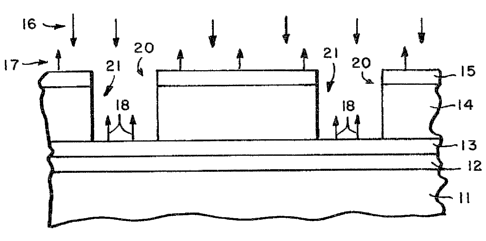
With reference to the Figures, Fig. lA depicts a
workpiece 10 which may be used in connection with the new laser
lithographic technique. The workpiece includes a substra~e
8b
.~
~ ;~791~)4
83-367
_g_
11 on which prior processing may have been performed before
the laser processing technique described herein has begun.
In the workpiece 10 depicted on Fig. 1, prior processing has
been perormed to deposit a layer 12 on top of substrate 11.
In addition, in previous processing, various features and
electronic circuit elements which are not specifically shown
in Fig. 1 may have been formed in substrate 11 and layer 12
by means of conventional processes which form no part of the
invention.
In accordance with the invention, a layer 13 is ini-
tially deposited on the layer 12, a third layer 14 in which
a recess is to be formed by means of laser radiation
(represented by downwardly-going arrows 16) is then
deposited on layer 13, and a top layer 15 is then formed
over layer 14. Layer 15 is patterned to form openings 20
IFig. lB) in the layer, which serves to expose portions of
underlying layer 14. The layer 15 can be patterned by, for
example, conventional photolithographic techniques using
chemical or ion beam etch procedures. The openings 20 are
provided to define the sidewall boundaries of the recesses
which are to be formed in underlying layer 14. Two such
openings 20 are depicted in Fig. lB. The openings may be of
any arbitrary shape.
7 9 1~
83-367
-10-
The laser which will be used is selected so that the
materials which comprise layers 13 and 15 are highly reflec-
tive at the wavelength of the laser radiation. The material
which comprises layer 14 is selected to h ve low reflec-
tivity, and also low transmissivity, at the wavelength of
the laser radiation. As shown in Fig. lC, since layer 15 is
highly reflective at the wavelengths of the incident laser
radiation 16, layer 15 reflects laser radiation as
represented by arrows 17 and thus is not effected by the
radiation~ However, layer 14 does not reflect the radia-
tion, and thus the regions exposed by openings 20 absorb the
radiation and are effectively vaporized thereby and thus
removed to form recesses 21. The removal of the exposed
portions of layer 14 continues until the underlying portions
of reflective layer 13 are exposed. Layer 13, like layer
15, reflects the laser radiation, as represented by arrows
18, and is also unaffected thereby.
Thus, the pattern of layer 15 determines the shape (as
viewed from a direction orthogonal to the exposed surface of
layer 15) of the recess in layer 14, and layer 13 effective-
ly serves to determine the maximum depth of the recess in
the workpiece by preventing laser radiation from impinging
on layer 12. Accordingly, it is apparent that the recess
will not extend into layer 12 or substrate ll.
~9lt~
83-367
While the pattern of layer 15 has been described as
being formed in situ, that is, while layer 15 has been in
place on the workpiece, it will be appreciated by those
skilled in the art that layer 15 may comprise a mask which
has been patterned prior to being placed on laye~ ~
It will be appreciated that in certain circumstances it
may be undesirable for the etch-stop layer 13 to extend
throughout the entire workpiece 10. For example, if copper
is selected as the layer 13, and if layer 13 extends
throughout the workpiece, the copper would act as an elec-
trical conductor throughout the entire workpiece. If the
workpiece is to have electrical connections through the
openings 21 in layer 14, it would clearly be undesirable for
layer 13 to extend to all of the openings. ThuS, it may be
necessary to also pattern etch-stop layer 13 so that the
layer effectively complements the openings in layer 15.
This would suffice to eliminate electrical conduction paths
through layer 13 between the openings 21.
The materials selected for layers 13, 14 and 15 depend
upon the laser to be used in the process, or alternatively,
the laser selected for use in the process depends on the
types of materials which may be required for the workpiece.
In one particular example, the substrate 11 may comprise a
, . .
~;~79104
83-367
-12-
high density ceramic substrate having about seventy percent
alumina (Al2o3) and thirty percent titanium carbide, and
layer 12 may comprise alumina, and it is desired to produce
a recess in a layer 14 also comprised of alumina.
Continuing with the aforementioned example, a carbon
dioxide (CO2) laser may effectively be used since the ab-
sorption by alumina of the carbon dioxide laser radiation isvery high; that is, the alumina comprising layer 14 readily
absorbs radiation in the wavelengths emitted by the carbon
dioxide laser, and thus the exposed areas of layer 14 will
effectively be evaporated by the laser. Suitable material
for layers 13 and 15 in that example are copper and gold,
both of which reflect on the order of ninety-eight percent
of radiation in the wavelengths produced by carbon dioxide
lasers. In one particular example, layer 13 may be gold and
layer 15 may be copper, with both materials being deposited
on the respective underlying layers by means o~ sputtering,
and with the copper layer 15 being easily patterned by means
of ion beam or chemical etching techniques.
It will be appreciated that this method provides a num-
ber of benefits over conventional etching methods. In par-
ticular, the laser etching typically removes unwanted
material much faster than can be achieved by means of chemi-
~9~()4
83-367
-13-
cal etching techniques and with none of the undercutting
problems that are present. The new laser technigue may
cause some minor deformations due to thermal energy being
conducted in the vicinity of the openings in the workpiece
outside of the region being removed, and further to
resolidification of some of the melted material, but these
can be minimized as explained below.
The new laser etching technique does not rely on dif-
ferential etch rates between the masking material and the
material to be etched, as do ion beam etching techniques.
Accordingly, the minimum thickness of the mask used in the
laser technique is not related to the thickness of the
recess to be etched, as is the case in connection with ion
beam techniques. The reflective layers used in the laser
etching technique must be of sufficient thickness to be
reflective over the surface of the workpiece in the areas
not to be etched.
Furthermore, the new laser etching technique does not
require focusing of the laser beam to a small spot and
moving it over the surface of th~ workpiece to define the
required features, as is necessary in present laser etching
techniques. Thus, the sophisticated optical systems charac-
teristic of present laser techniques are not required in the
9~34
83-367
-14-
new technique. In addition, the minimum feature size is not
related to the size of the laser spot, and the workpiece can
be processed at one time since the new technique allows the
entire surface of the workpiece to be processed at one time.
As has been noted, recesses formed by the the new laser
lithographic technique may be slightly deformed due to heat-
ing of the workpiece outside the region being removed, and
also due to resolidification of material which was heated by
the laser but not evaporated, which could limit the resolu-
tion of the work. In addition, some metal and ceramic
materials may deform and some ceramic materials may crack
under intense laser radiation. However, these problems can
be minimized by immersing the workpiece in a liquid, or
providing a layer of liquid over the irradiated surface of
the workpiece, while the laser is irradiating the surface.
The liquid can act both to cool the workpiece and, depending
on the nature of the liquid, may also either dissolve, by
chemical action, or flush away, by mechan~cal action, debris
that is thrown up from the workpiece while the laser is
entrained thereon.
As will be appreciated by one skilled in the art, the
selection of a suitable liquid will depend on a number of
factors. In particular, a suitable liquid should be ~airly
,
2 ~ 91~ 83-367
-15-
transparent to the laser radiation and should not react with
the masking material (that is, layers 13 and 15 in Fig, 1).
It is also preferable that, if the liquid reacts with the
material being etched (that is, layer 14 in Fig. 1) at all,
it should react only very slowly at room temperature, so
that the workpiece itself not be etched by the liquid out-
side of the area on which the laser beam is impinging.
If the liquid reacts with the material to be etched at
elevated temperatures, which would be present at the areas
illuminated by the laser radiation, it may assist the etch
operation, effectively performing a chemical etch on the
material in the area being struck by the laser. Since the
temperature of the portions of the material that do not
directly receive laser radiation will not be increased as
much as the portions that do, they will not be etched as
much by the liquid. The resulting etch by the liquid, which
is effectively a chemical etch, would be more anisotropic
than is a conventional chemical etch.
.,, . ~ .
1~9~L04
83-367
-16-
EXAMPLES
Example No. 1
Etching of Alumina by CO2 Laser
An alumina layer was formed on a substrate, and a 200
Angstrom layer of chromium was deposited by sputtering. The
chromium layer was provided to act as an adhesion layer for
the next layer, which was gold (alternatively, copper could
have been used). The gold layer, which served as layer 13
(Fig. 1) was one-half micron thick. A sheet of alumina ap-
proximately thirty to forty microns thick was then deposited
by sputtering to form layer 14, and a three-tenths to five-
tenths micron thick layer of copper (alternatively gold
could have been used) was sputtered as layer 15.
The copper layer (15) was then patterned by conven-
tional photolithographic techniques. In one case, a layer
of photoresist was deposited on top of the copper layer and
patterned in a conventional manner exposing a pattern of ths
copper layer underneath. The exposed copper was etched by
an ion beam etch and any photoresist was dissolved in a de-
veloper. This leaves the openings (20, Fig. 1) exposing
alumina in layer 14.
In another case, the copper layer 15 was patterned
using a conventional lift-off technique. In that technique,
, . .. .
~ 79~
83-367
-17-
the photoresist layer was deposited before the copper layer
~the photoresist layer is not shown in Fig. 1) and a pattern
in the photoresist was exposed in a conventional
photolithography step. A thin copper layer was then sputter
deposited on top of the photoresist, and the patterned
photoresist was dissolved in a developer. The dissolving
photoresist took with it the copper directly on top, leaving
the copper in the desired pattern.
After the copper layer 15 was patterned, the workpiece
was covered by a thin film of methylene chloride liquid and
irradiated using a pulsed carbon dioxide laser to etch the
exposed alumina. The energy supplied by the laser was about
four Joules per laser pulse at four to ten pulses per second
over an area of approximately one-fourth square inch.
Example No. 2
Etching Using A Removable Mask
In this example, the mask comprising layer 15 was not
deposited onto the workpiece, but instead was formed sepa-
rately and placed onto the surface of the workpiece to be
etched. A workpiece was formed of alumina. A base mask was
formed of generally planar nickel, with openings through
791~34
83-367
-18-
which the workpiece could be exposed. The mask had a thick-
ness of about fifteen microns in the areas adjacent the
openings, and elsewhere a thickness of about 125 microns,
the thick portion providing mechanical sturdiness while the
thin portion allowed for better resolution in alignment of
the mask over the workpiece. To prevent chemical interac-
tion between the mask and a liquid which might be used, the
mask was plated with a ten micron layer of gold. The mask
was then aligned with the workpiece and both were clamped
together in a fixture. Methylene chloride liquid was then
sprayed onto the fixture to form a uniform thin layer on the
surface which would receive the laser radiation.
The workpiece was then illuminated by a CO2 laser. To
increase the energy per unit area of the laser (which had
about four Joules per pulse), the laser beam was focussed to
a size of about one-fourth inch by one inch by means of
lenses, and the workpiece was moved under the laser beam at
a rate of six-thousandths of an inch per second until the
entire surface of the workpiece had been exposed through the
mask. The process was repeated twenty times to form
recesses in the alumina having a depth of approximately
thirty-five microns.
` ~X791()4
83-367
--19--
After the process was concluded, the mas~ was removed
from the workpiece by unclamping the fixture. The mask
could be used in a subsequent etching process.
Example No. 3
Etching of High-Density Ceramic
A workpiece was fabricated of high-density ceramic hav-
ing a patterned layer of copper to define the pattern to be
etched. Carbon dioxide, ruby and Nd:YA5 lasers were used to
perform the etch. When the etch was performed in air, that
is, when no liquid was present, small cracks developed in
the ceramic and some ceramic debris from the etch
resolidified.
In other trials using high-density ceramic, several
liquids were used, including methylene chloride and a solu-
tion of potassium hydroxide in water. The potassium
hydroxide solution was generally satisfactory for the Nd:YAG
and ruby lasers, even though for some depths of liquid it
absorbed about thirty-five percent of the radiation of the
Nd:YAG laser. The preferred concentration of the potassium
hydroxide was on the order of twelve normal (12N) or above;
trial etches in solutions having concentrations of on the
order of six normal or less exhibited some cracking of the
ceramic.
1 2~9~V4
83-367
-2~-
~xample No. 4
Etching of Permalloy
A workpiece was prepared comprising an Alsimag sub-
strate on which a three thousand Angstrom thick layer of
aluminum was deposited by sputtering. The aluminum served
as an etch-stop layer. A two thousand Angstrom thick layer
of permalloy was then plated onto the aluminum sheet. An
aluminum mask was formed on the permalloy layer using a
lift-off technique. The workpiece was then irradiated, in
air, with a krypton fluoride laser. The permalloy was
etched without affecting the aluminum mask or the etch-stop
layer.
In another trial, a solution of dilute nitric acid with
small amounts of potassium dichromate was used. The result-
ing etch had less resolidification of molten permalloy than
had occurred in the etch without the liquid.
5,
Example No. 5
Etching of Poly~er
A thin film of copper was deposited on a silicon sub-
strate as an etch-stop layer (13, Fig. 1). A layer of
photoresist was deposited on the copper layer and baked
,
.
~ ;~79104
60~12-1794
hard. A portion of the photoresist layer was exposed to ruby
laser radiation through a hole in a removable stainless steel
mask. The laser beam had an effective diameter of about 3
millimeters, and the hole in the mask had a diameter of about 40
microns. The portion of the photoresist struck by the laser was
effectively decomposed into volatile parts, and so no
resolidification occurred. The copper effectively stopped the
etch, but was somewhat deformed by the high energy of the ruby
laser radiation.
The foregoing description has been limited to specific
embodiments of this invention. It will be apparent, however, that
variations and modifications may be made to the process, with the
attainment of some or all of the advantages of the invention.
Therefore, it is the object of the appended claims to cover all
such variations and modlfications as come within the true spirit
and scope of the invention.