Note: Descriptions are shown in the official language in which they were submitted.
79~6
DIGITAL SEQUENCE POLaRITY DETECTION WITH
ADAPTIVE SYNC~RONIZATION
Technical Field
This invention relates in general to synchronous
digital communication systems and in particular to
determining the polarity of and synchroni~ing to received
digital data.
Background Art
Some of the decisions in the design of synchronous
digital communication systems involve the method of
encoding source bits and the method of synchronizing
decoding processes in the receiver for correct recovery
of the transmitted message.
In a binary data system, each bit received from the
channel can be one of two possible symbols. Without
a priori knowledge of polarity inversions that the bits
may have encountered in crossing the channel, the
receiver lacks the information necessary to decode the
individual bits. Inversions may occur when the data is
modulated by frequency shift keying (FSK) and the signal
undergoes frequency translations in being sent across the
channel. In FSK modulation, a positive frequency shift
of the carrier corresponds to one binary symbol, and a
negative shift corresponds to the other. Frequency
,
1;~79116
- 2 -
translations during up- or down-conversions associated
with radio transmission or with multiplexing for
telephone line transmission may not preserve the meanings
of positive and negative frequency modulation shifts.
onQ of the methods used in the prior art to preserve
polarity information across a channel is known as
differential encoding. The signal is encoded o that
information resides in the difference of polarity from
one bit to the next. Using this method avoids the need
for a coherant, local phase reference, since each bit
serves as the local reference for the succeeding bit.
Differential ancoding trades noise performance for
reduced system complexity. An error in one bit extends
to the next, for if an error occurs in one bit, the
receiver has an uncertain reference and may not correctly
decode the next bit. By degrading error performance,
differential encoding may interfere with system
operation. In particular, it may diminish the
effectiveness of error correction circuits.
The present invention also addresses the method of
synchronization used in a communication system. What
method i5 used can affect the ability of the receiver to
detect sequences transmitted over the channel for various
identification purposes, to maintain or quickly regain
synchronization in an noisy channel environment, and to
quickly adapt to changes in delay characteristics of the
transmission channel. Prior art design choices have
frequently involved tradeoffs,-in which improvements of
one aspect of synchronization performance have meant
degradation of another.
An example of transmitting sequences for
identification occurs in a synchronous stream encryption
system. The transmitter encrypts source bits with a
pseudo-random keystream sequence; the receiver decrypts
them by an inverse operation. Each channel bit produced
791~
-- 3 --
depends only on its position in the stream of source bits
and on the particular keystream in use. To recover the
source bits, the receiver must regenerate the keystream
locally and align it with incoming channel bits.
To enable the receiver to regenerate and align the
keystream, the transmitter sends an identi~ying sequence.
Not knowing when the sequence will be sent, the receiver
must be able to detect the sequence in the presence of
random digital data. Detecting a sequence can serve a
variety of other purposes. For example, to increase the
certainty that the receiver has correctly identified a
synchronization or timing mark imbedded within noisy
data, the system may require that the receiver have
previously detected a unique sequence.
A different aspect of synchronization that the
present invention addresses is how the receiver initially
establishes synchronization when communication begins and
how it maintains synchronization during interruptions of
communication. When error correction is used to improve
the certainty of synchronization in a noisy environment,
initial synchroni~ation i9 often a slow process. Error
correction circuits must process a number of bits to
reach full effectiveness. Synchronization attempts made
shortly after transmission begins or after recovery from
a fade use less certain bits and may, therefore, be less
reliable than later attempts, which can use more certain
bits.
Delaying synchronization also helps the receiver
adapt to changes in delay characteristics of the
transmission channel that occur after communication has
been established. on type of delay change contemplated
by the invention is found in a multiple site system with
receivers situated at diverse geographic sites to obtain
wide area coverage of the transmitted signal. Each of
7911~
-
-- 4 --
the receivers sends demodulated output to a central
control point that chooses one signal path, according to
signal quality, to supply the data decoding circuits.
The time scales may be misaligned among the data signals
received from the ~everal sites because of propagation
differences in the paths from the transmitter to each of
the receiving sites or differences in the electrical
paths from the remote sites to the control point.
Synchronization may be disrupted if the path selection
changes after a message commences.
In a typical scenario, thls receiver selection occurs
shortly after a message begin~s. The initial selection
may be changed before being made final. Synchronization
rapidly acquired at the start of the message might later
become incorrect if the selection changes. Under these
circumstances, it is desirable for the synchronization
system to be able to rapidly and automatically readjust.
Delaying synchronization affects the ability of the
receiver to quickly recover from momentary communication
impairments, so prior art designs have often employed
hysteresis to provide adaptive timing. Hysteresis
prevents the receiver from attempting to reestablish
synchronization, with its attendant delay, if it has been
interrupted for only a short time. An example of
hysteresis may be found in a communication system
designed for a terrestrial radio channel that may be
subject to momentary fading. During a fade, the receiver
may be unable to continue to recover synchronization
information yet have sufficient short-term stability to
continue to correctly decode channel bits. Without
hysteresis, the receiver would attempt to reestablish
synchronization each time it recovered from a fade.
A problem experienced with hysteresis is that it
prevents the receiver from responding to synchronization
91~ '
- 5
changes until the hysteresis interval has elapsed. This
interferes ~ith the ability to respond rapidly, as
required in a multiple site receiver system.
Summary of the Invention
It is an object of this invention to overcome the
foregoing deficiencies in prior art digital communication
systems in determining polarity of digital channels and
in reliably establishing and maintaining synchronization.
In particular, it is an object of this invention to
provide an improved method for determining the polarity
of a received digital data stream without adversely
affecting the performance of error correction circuits.
It is a further object of this invention to provide
an improved method for detection of synchronization
sequences by being able to quickly readjust after initial
synchronization and tolarate path delay shifts that occur
soon after transmission begins.
It is another object of this invention to provide a
synchronization method that can rapidly reacquire
synchronization after it has been interrupted momentarily
because of transmission impairments.
According to the invention, the transmitter in a
digital communication system sends a synchronization
sequence that uniquely identifies the polarity of tha
data. From the received data, the raceiver produces
non-inverted and inverted polarity data streams that
couple to like synchronization detectors. Only the
detector to which the correct polarity data stream is
coupled responds. Logic circuitry determines which
detector responds and, accordingly, selects the polarity
of received data to be further processed by the receiver.
~2'7911~i
-- 6
After polarity is established, both detectors monitor
the received data stream of the selected polarity to
determine whether synchronization shifts after having
been initially established. Monitoring continues until
terminated by other recei~er circuits.
Brief DescriPtion of the Drawinqs
The features of the present invention that are
believed to be novel are set forth with particularity in
the appended claims. The invention, together with further
objects and advantages thereof, may be understood by
reference to the following detailed description taken in
conjunction with the accompanying drawings, in which:
Figure 1 is a block diagram of a synchronization
sequence detector that includes error correction and is
of the type used in the embodiment of the invention:
Figure 2 is a block diagram showing in greater detail
the sequence correlation circuits of Figure l; and
Figures 3A a~d 3B are block dia~ra~s of a polarity
a~d sy~chronization ~equence detector collstructed in
accordance vith the pr~ser~t il~ve~tion.
Detailed DescriPtion of the Invention
Af~tcrisks (*) in thi~ sr)ecif`ica~t.ion arc p~rt Or
the signal ~ame (eg. SNYC-DETECT*) and do not indicate
footnotes or further definitions.
The invention is shown as part of a synchronous
digital communication system, which incll~des: a
transmitter, a communication channel, and a receiver.
The transmitter sends a sequence for purposes of
identifying channel polarity and providing
synchronization information. The sequence will not be
detected if it is inverted. The receiver creates non
inverted and inverted data streams from the received
signal and couples them to two like sequence detection
'79'~16
-- 7 --
circuits that can respond to the transmitted sequence.
Regardless of the net polarity through the channel from
transmitter to receiver, one of the two data streams will
have net non-inverted polarity, and the sequence detector
to which it is coupled will ~e able to respond to the
sequence. Logic circuitry determines which has responded
and selects that polarity of data for further processing
in the receiver.
The method used for sequence detection is to locally
generate a sequence that is based on a portion of the
received data stream and that is continued according to
the algorithm by which the transmitter generates its
identifying sequence. Error correction circuitry
estimates errors that may have corrupted the sequence
during transmission and corrects them to the extent
possible. The detector correlates the data stream and
local sequence during an interval that is shifted either
ahead or behind the portion of the error-corrected data
stream used to initialize the local se~uence generator,
t~ereby avoiding the region during which short-term
correlation between the data stream and local sequence
would otherwise cause false indications of detection when
only noise or random data is being received. Although
not shown here, the logic circuitry may provide switching
so that the detector that has responded can provide its
locally generated sequence to receiver circuits for
further processing.
After one detector responds, which establishes
polarity, the logic couples both detectors to the input
stream of the selected polarity. The logic circuit
monitors both detectors, and if the other detector
responds, the logic circuit selects it, instead of the
first detector to have responded, for providing the
locally regenerated sequence to the receiver circuits.
-- 8
Also, after a detector has responded, hysteresis in the
logic prevents that detector from immediately changing
its locally regenerated sequence but allows the other
detector to quickly respond to synchronization changes.
The operation of the sequence detectors is readily
explained with reference to Figure 1, which isolates one
detector. The detection circuit of Figure 1 is the
subject of United States Patent No. 4,667,327, entitled
"Linear Feedback Sequence Detection with Error
Correction", which issued May 19, 1987, to Bright et al
and assigned to the assignee of this application.
Figure 1 shows a transmitter, which includes a
source 402 of arbitrary serial data 404, a generator 406
for developing a synchronization sequence 408, and a
switch 410 that selects, on command of control line 412,
either the source data or the synchronization sequence
for output at 414 onto a communication channel 416. The
sequence generator is a linear feedback shift register
(LFSR) that generates a pseudo-random, maximal length
sequence according to characteristic polynomial, C(x),
where:
C (X) = 1+X15+X27+X38+X46+X62+X64
Outputs from shift register stages corresponding to
non-zero terms in the polynomial add in exclusive-OR
gates 420, 422, 424, 426, and 428 to form parity signal
430, which feeds back to the first stage of the register
at 432. Those skilled in the art will appreciate that
the length of the shift register and the characteristic
polynomial are matters of design choice depending on the
particular application required.
The output of the transmitter reaches the receiver
at 418 via communication channel 416. The receiver uses
1'
791~t~
circuit 100 to estimate ancl, within limits, correct
errors in a shift register synchronization sequence. No
provision is made here to correct errors in random serial
data. A suitable embodiment for circuit 100 is fully
described in U.S. Patent 4,667,327 entitled "Error
Corrector for a Linear Feedback Shift Register Sequence,"
issued May 19, 1987 and assigned to the same assignee as
the present application. The circuit will be only
briefly described here.
The received bits shift into register 110 at input
102. Exclusive-OR gates 120, 122, 124, 126 and 128,
arranged according to the characteristic polynomial used
in the transmitter, combine outputs of the register to
form a parity bit at 132. The parity bit does not feed
back into the register 110; instead, it drives one side
of exclusive-OR gate 116, which compares the parity bits
with the received bits. When the expected LFSR sequence
is received, each parity bit and corresponding incoming
bit should agree a difference indicates either that the
received bit is not from the expected sequence or that
the bit is from the sequence but has been corrupted by
noise.
A difference causes exclusive-OR gate 116 to
indicate a logical true level. Successive bits from gate
116 shift through gate 118 into syndrome register 112.
Selected outputs of the syndrome register represent past
estimated errors and feed majority threshold decoder gate
114. The majority gate also received the most recent
estimated error from signal 104, which improves the
ability of the circuit to correct errors under high error
rate conditions. The decode threshold is l greater than
a majority to account for this additional input.
1;~'79~
-- 10 --
When sufficient estimates of error in ths syndrome
register 112 coincide with the taps feeding the majority
gate 114, its output 134 asserts, indicating that an
error has been estimated in the bit at 138 that is at
this time being shifted out of register 110. Signal 134
corrects the bit by complementing it in exclusive-OR gate
130, maXing corrected bits available at 136.
Additionally, signal 134 complements the error terms as
they shift into succeeding stages in the syndrome
register 112 and complements signal 104 as it passes
through gate 118 to feed into the syndrome register at
106. This is known as s~ndrome resetting, which has the
effect of removing error terms greater that the length of
the shift register and which further improves the error
correction capability of the circuit.
As the corrected bit stream becomes available at 136,
the receiver searches for tha LFSR se~uence by performing
several steps. First, it loads a portion of the
corrected bit stream into shift register 302. Next, it
locally regenerates an LFSR sequence continuing from that
initial load, using a parity tree to provide feedback at
332 according to the characteristic polynomial in the
transmitter. At the same time, it derives a sequence
shifted from that in register 302, using future bit
25 parity tree 336 to provide the shifted sequence at 356.
Finally, it correlates the shifted sequence at 356 with a
correspondingly shifted input sequence at 358, using
detector 200 and sync detect latch 222 to indicate by
signal sync-detect* at 310 whether the received signal
is the expected LFSR sequence.
If the initial load in closed-loop register 302 were
incorrect to generate the LFSR sequence, detector 200
would fail to indicate detection. In that event,
register 302 would have to be reloaded for a new attempt
1~7~
to generate the sequence. The preferred embodiment uses
a parallel loading arrangement that saves time and can
give more chances to reload when only a limited number of
bits of the LFSR sequence are transmitted. To shift out
the incorrect bits from rsgis1:er 302 and refill it in
serial would require shifting in 64 new bits. However,
by loading in parallel, new bits replace incorrect bits
in a single operation and save the time otherwise needed
for 64 shifts.
The length of the correlation interval is 48 bits.
After correlation, 48 bits will have shifted into
register 302 from the feedback parity tree at 332 and
must be replaced. Sixteen of the initial 64 bits will
have been shifted by 48 places, but they will remain in
register 302 and may be kept. During the correlation
interval, temporary shift register 306 receives 48
error-corrected bits in serial at 304 and stores them.
Then, on command from line 314, the parallel load
operation sends 48 new bits on bus 308 from reglster 306
to replace the 48 feedback bits in register 302, leaving
the other 16 bits in place.
To form the parity bit 330 that feeds back at 332 to
regenerate the LFSR sequence, exclusive-OR gates 320,
322, 324, 326, and 328 add outputs of register 302
selected according to the characteristic polynomial used
in the transmitter. ~ach parity bit computed is the next
bit in sequence following the 64 bit vector initially
loaded in shift register 302.
Future parity tree 336 provides at 356 a sequence of
bits shifted ahead of the sequence of parity bits feeding
back at 332 to register 302. The polynomial, P(x), to
compute the parity sequence shifted by (i) bits may be
determined from the characteristic polynomial for the
sequence, C(x), as:
P(x) = x~(i+l) mod C(x),
~'~791~6
- 12 -
where positive values of index (i) mean a shi~t to the
future, and negative values mean a shift to the past.
In other words, P(x) is the remainder after dividing
x~(i+l) by the characteristic polynomial C~x). For a
shift of 25 bits to the future, i = +25, and:
P(x) = xl+x4+xl2+xl6+x2o+x27~x3s
+X36+X38~X5l+x53,
The polynomial terms indicate how to combine taps on
the intermediate stages of shift register 302. A zero
degree term would correspond to the output of the first
stage of the register, a first degree term would refer to
the output of the second stage, and so on until a 63rd
degree term, which would indicate the output of the 64th,
or last, stage of the register. A zero coefficient would
indicate to ignore that output; a non-zero coefficient
would indicate to include that particular intermediate
output in the parity sum. For example, to compute the
sequence shifted 25 bits into the future requires ten
exclusive-~R gates to sum the eleven non-zero terms in
the polynomial P(x~. Exclusive-OR gates 340, 342, 34~,
346, and 348 through 35~ represent the parity tree.
A version of the input sequence shifted by an amount
corresponding to the future parity sequence is obtained
by taking a tap ahead of the output stage of register
110. The feedback parity sequence 330 corre~ponds in
time to the bit sequence coming out of the open loop
register 110 at 138 and available with error correction
at 136. Register 110 delays the input sequence by 64
bits, so a sequence shifted ahead by the equivalent shift
in the future parity tree, up to 64 bits, is available at
one of the intermediate stages in the register. To
obtain a shift of 25 bits~ line 158 takes the input
sequence from tap 39 of the register, 25 bits ahead of
the output at the 64th stage.
~791~ .
- 13 -
Finally, the two sequences are correlated during a
suitable measuring interval. Exclusive-OR gate 360
compares corresponding bits from the two sequences
coupled to it on lines 356 and 358 and indicates errors
by logical true on output 362 whenever they differ.
Detector 200 accumulates the comparisons for a
predetermined number of bits and indicates detection if
the number of disagreements is less than a selected
limit.
Figure 2 shows details of synchronization detector
200, sync loss counter 240, and miscellaneous logic
circuitry for internal resetting and for providing output
signals 310 and 312. In response to a clock synchronized
with the sequences and supplied at pin 231, window
counter 216 counts towards a terminal count, which
defines the correlation interval and is chosen here as
48, while the error counter 214 accumulates error
indications supplied by line 362 to its clock pin 229.
Delay flip-flop 217, coupled to the terminal count output
1232 of the window counter, delays and holds that output
on line 232 for one clock period. Whichever counter
reaches terminal count first resets both by sending its
terminal count output through OR gate 225, whose output
resets the error counter at 228 and the window counter at
230. When the error counter reaches terminal count, line
225 pulses only momentarily, as the reset clears the
terminal count. When the window counter resets, the
pulse at 232 holds for an entire clock period, which
facilitates the timing of circuits coupled to it.
To initialize and start the detector from a known
state, an externally supplied reset signal momentarily
goes high and couples on line 243 through OR gate 244 to
reset sync detect latch 222, which forces a logical true
on the Q* output 224. The reset signal also clears the
1~79il~i .
- 14 -
delay flip-flop 217 and resets the srror and window
counters through OR gate 226. Now, if sufficient error
counts arrive on line 362 for the error counter to reach
its terminal count before the window counter resets it,
the error counter momentarily asserts line 225, which,
combining in AND gate 238 witll the logical true on line
224, sends a parallel load pulse on line 312 to shift
register 302 at pin 314, shown in Figure 1. Upon
receiving the parallel load s:ignal, register 302 reloads
from the contents of temporary register 306 and begins
generating a sequence from the new load vector.
In contrast, if few error indications arrive on line
362, the window counter will reach its terminal count
before the error counter does and will assert line 1232.
A high will appear on 232 one bit time later, which sets
latch 222 at pin 234, and output 224 negates, which
inhibits gate 238 from sending a parallel load siynal to
the shift register. The sequence generator continues to
generate the sequence according to its initial load
vector. Sync-detect* 310 negates, indicating that the
LFSR sequence has been detected.
Sync loss counter 240 provides detection hysteresis,
which allows sync detector 200 to accept momentary bursts
of errors in the received sequence or to fail to detect a
predetermined number of synchronization sequences in the
message format without immediately removing indication of
detection. Each time window counter 216 reaches terminal
count, line 232 asserts after a delay and triggers line
235 to reset sync loss counter 240, which itself counts
clock pulses supplied at pin 233 from the master clock.
A~s long as the correct LFSR sequence continues to arrive,
the window counter will reach terminal count and provide
an output at 232 before the error counter can reset it.
- ~79 L~;
- 15 -
If the correct LFSR sequence stops arriving, error
counter 214 begins to accumulate a su~ficient number of
counts to reach its terminal count before the window
counter resets it, and the error counter will force both
the window counter and itself to reset. This prevents
the window counter from resetting the sync loss counter,
which continues towards its own terminal count. If
errors continue to occur in each window period for longer
than the predetermined hysteresis interval, sync loss
counter ~40 reaches terminal count, asserts its output at
242, and resets latch 222 at pin 220. The Q* output
224 asserts, indicating loss of detection on 310 and
removing the inhibit from gate 238. Gate 238 will be
able to pass the parallel load pulse when the error
counter next indicates an accumulation of errors.
Those skilled in the art will appreciate that the
circuits shown in Figures 1 and 2 represent just one way
to detect sequences and that other detectors may be
substituted.
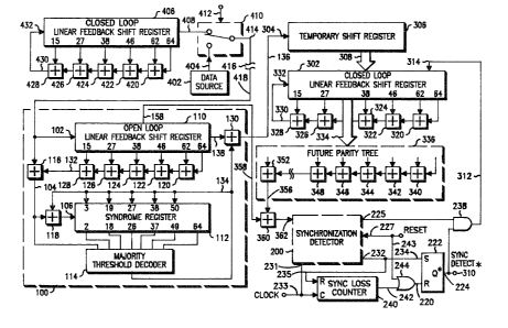
Figure 3 now shows the preferred embodiment of the
invention in its entirety. Two sequence detectors are
provided and are indicated by similar reference numerals,
with primed numerals indicating the detector that
initially monitors inverted polarity received data. The
data stream from the transmitter at 414 crosses channel
416 and reaches the receiver at 418. The non-inverted
data stream couples to error correction circuit 100 on
line 420. Circuit 100 is identical with that described
in the discussion of Figure 1 and includes open-loop
register 110, the parity tree for generating parity bit
132, syndrome register 112, decoder 114, and exclusive-OR
gate 130. Circuit 100 provides the delayed input
sequence at 138, the shifted input sequence at 158, and
the error-corrected output at 136.
7911~
.
- 16 -
As suggested by the dashed line, inverter 419 could
be used to invert the input stream and provide inverted
polarity, received data strea~ 420' to error-correction
circuit 100' in like manner as line 420 couples
non-invertad data to circuit 100. However, it will be
recognized that the open-loop regi~ter 110 and the parity
tree providing the sequence at 132 perfor~ linear
operations on the input data stream. Circuit 100' need
not be duplicate these linear functions, since inversion
performed before or after linear operations has the same
effect. Thus, rather than obtaining ths input signal to
circuit 100' from inverted data stream 420', the output
104 of exclusive-OR gate 116 may be inverted at 105 to
directly provide the inverted error estimate 104'.
Furthermore, the delayed input sequence at 138 may be
inverted at 139 to produce inverted, delayed input
sequence 138'. The inverted, shifted input seguence,
indicated as 158x', is unavailable, since the open-loop
register 110' is not used in this embodiment. Instead,
inverter 159 derives sequence 158' from sequence 158.
Avoiding duplication of the shift register and parity
tree saves considerable circuitry, which may be
advantageous in an implementation of the circuit. Those
circuits performing non-linear functions, in particular,
the majority threshold decoder and syndrome register, are
not redundant and must be duplicated.
Switches 137, 161, 137', and 161' can direct the
error-corrected and shifted sequences to either of the
synchronization detection circuits. Initially, non-
inverted signals couple to detector 200, and inverted
signals couple to detector 200'. once polarity detection
occurs, the logic circuitry couples the sequences of the
selected polarity to both detectors and ignores the
sequences of the other polarity. Also, the logic
911~:i
- 17 -
circuitry selects which polarity of input signal, 418 or
418', will supply other circuits in the receiver at 422.
To initialize the logic and correlation circuits, an
externally supplied signal provides momentary reset
pulses. The pulses on lines 227 and 227' reset the
counters in synchronization detectors 200 and 200',
respectively; the pulse on line 243 drives OR gate 244
high to reset the sync detect latch 222, the polarity
latch 60, and the last detect latch 40. Sync detect
latch 222 provides a high at sync-detect* output 224,
and it provides a low on Q output 84. Polarity latch 60
provides a low at its Q output 70, which couples on line
16 to switches 161 and 137 and places them in the state
indicated by (0). These switches couple the non-
invert~d, shifted sequence 158 and error-corrected
sequence 136 to sequence detection input lines 358 and
304, respectively. Polarity latch Q output 70 combines
in exclusive-OR gate 72 with the Q output 84 of the sync
detect latch and provides a logical low on line 16' to
switches 161l and 137' to place them in the (0) state.
These switches couple the inverted sequences 158' and
136' to detector input lines 358' and 304', respectively.
Sync-detect* output 224 also enables AND gate 64 and
passes on lines 54 and 54' through OR gates 52 and 52' to
enable gates 58 and 58' and their parallel load lines 314
and 314', respectively.
Enabling the load lines allows both the sequence
detectors to search for the transmitted LFSR sequence.
If the net channel polarity is non-inverted and the LFSR
sequence is being received, detector 200 responds. Line
310 goes high and drives OR gate 32 high~ Delay element
34, clocked one half bit period later by the inverted
clock 36 from inverter 35, produces a high at 38 that
passes through enabled AND gate 64 to clock the polarity
t~9~
- 18 -
latch 60 at pin 62. The polarity latch captures the low
at its D input from line 311 and produces a low on Q
output 70. Line 70, connecting by line 16 to switch 18,
causes it to select non-inverted data onto line 422,
which can supply other receiver circuits (not shown
here).
once detection has occurred, the output of polarity
latch 60 will not change unless sync is lost. The high
signal 38 from the delay element 34 sets sync detec~
latch 222 at pin 234, pulling sync-detect* line 224
low, disabling AND gate 64 an~ preventing further
clocking of the polarity latch. The Q output 84 of the
sync detect latch goes high, which causes exclusive-OR
gate 72 to invert the signal on line 70 and send a high
on line 16' to switches 137' and 161'. These switches
will select the (1) state and connect non-inverted
polariky se~uences to synchronization detector 200' and
its associated circuitry. This means that detectors 200
and 200' now both search the non-inverted polarity data
lines.
The inverted output at 311 from synchronization
detector 200 also goes on line 48 to the D input of the
last detect latch 40. On line 42, the Q output from
delay element 34 clocks the last detect latch, which goes
low on Q output 44 and high on Q* output 46. Line 54
will be low, because sync has been detected, so line 44
going low causes OR gate 52 to send a low on 56 and
disable parallel load signals through AND gate 58. This
prevents detector 200 from reloading if it stops
receiving the LFSR sequence. Instead, it will continue
to generate a local sequence from its initial load.
In contrast, Q* output 46 from last detect latch ~0
couples through OR gate 52' and enables AND gate 58'.
Therefore, detector 200' may reload its local shift
register if it accumulates a sufficient error count
791~i
-
-- 19 --
and may quickly respond to changes in synchronization.
For example, in a multiple site receiver system, if the
channel dslay shifts because receiver selection changes,
detector 200 will continue to generate its sequence,
which will now be incorrectly synchronized with received
data. Detector 200' will lose synchronization and
reload. Once detector 200' reloads, it will again be
able to detect the synchronization sequence, which it
will indicate by pulling line 310' high. This signal
will force OR gate 32 high, and a high will again be
clocked out of delay element 34 at Q output 38. Polarity
latch 60 will not change, as AND gate 64 is disabled;
however, last detect latch 40 will clock and sample its D
input, which will at this time be at a logical high, as
detector 200 has not pulled its detect line 310 high. Q
output 44 will go high and couple through OR gate 52 to
enable AND gate 58 and parallel loads to register 302.
Q* output 46 will go low and, combining with the low on
line 54', will force OR gate 52' low to disable AND gate
58' and cut off parallel loads to register 302'. The
roles of the two sequence detectors will have reversed:
detector ~00' may not reload; detector 200 continues to
search for shifts in synchronization and may reload if it
accumulates errors. The process of exchanging roles may
continue indefinitely or be terminated by an external
event. For example, the message may include a timing
mark in the message format to indicate the end of the
synchronization interval, or the receiver may use a timer
to terminate synchronization attempts after a
predetermined time.
This discussion has assumed that non-inverted
detector 200 was first to detect a sequence. If the
channel had inverted the received data, detector 200'
9~
- 20 -
would have been the detector that first recognized a
valid sequence. Line 310' would have gone high and
pulled OR gate 32 high, and delay element 34 would have
produced a high at 38 that would have clocked polarity
latch 60 and last detect latch 40. The polarity latch
would have sampled a high on line 311 and produced a high
at Q output 70. This would have pulled line 16 high and
set switches 137 and 161 to the (1) state, which would
have coupled inverted sequences 136' and 158' to detector
200. Also, signal 70 would have combined with signal 84
and sent a low from exclusive-OR gate 72 on line 16' ~hat
would have kept switches 137' and 1~1' in the ~0) state.
These switches would have continued to provide the
inverted sequences to detector 200'. Line 16 would also
have caused switch 18 to select inverted polarity data
stream 418' and provide it to receiver circuits at 422.
The embodiment shown in Figure 3 differs slightly
from the basic sequence detector shown in Figures 1 and 2
in the connection of the sync loss counter 240, which
provides hysteresis in the detection process. Rather
than being connected to the window counter output of a
particular detector, the sync loss counter 240 connects
to the output of OR gate 32. This signal combines the
window counter outputs of the two synchronization
detectors and goes high when either window counter
reaches terminal count. As long as one of the two
detectors continues to reach the end of the correlation
interval before too many errors accumulate, the sync loss
counter will be reset. If both detectors begin
accumulating errors, neither will reach window terminal
count and reset the sync loss counter. The sync loss
counter will eventually reach its terminal count and
reset the sync detect latch 222 on pin 220 through ~R
gate 244. Resetting the sync detect latch forces
~ ~791~i
- 21 -
sync-detect* 224 high and starts the entire polarity
and sequence detection process over from the beginning.
While a particular embodiment of the invention has
been described, it should be understood that the
invention is not limited to the embodiment shown, as many
modifications may be made. It is contemplated to cover
by the present application any and all such modifications
that may fall within the true spirit and scope of the
underlying principles disclosed and claimed herein.
What is claimed is: