Note: Descriptions are shown in the official language in which they were submitted.
~79381
D-8446 C-3681
Summary of the In ention
This invention relates to a phase shift
oscilla~or which may be used in two modes: (1) a fixed
frequency mode wherein the frequency of oscillation is
precisely fixed by a resonator such as a crystal and
(2) a variable freauency mode wherein the frequency of
oscillation may be varied from that determined by the
resonator in either direction in response to a control
voltage. Such an oscillator, when used in its first
mode, has the advantage of a stable predetermined
frequency of oscillation determined by the resonator
and a minimu~ of other circuit elements. It may be
placed in a second mode of operation, however~ by
activating other elements responsive to a control
voltage to vary the frequency of oscillation from the
predetermined freqency. The oscillator has utility, to
cite only one example, in a radio receiver, wherein it
ma~ be used in its first mode in one reception circuit,
as a fixed fre~uency oscillator, but may be used in its
~ second mode in a phase locked loop in another reception
circuit.
The prior art typically uses a single voltage
controlled oscillator to perform both sin~le and
multiple freauency operation; but sin~le frequency -
operation is subject to the variation of the control
voltage due to device and environmental changes, which
tends to vary the frequency of operation. Variable
crystal oscillators are also known, but they tend to
'
'
.
~7~;38~
include control voltages and extra phase shift networks
which are also subject to drift.
The oscillator of this invention comprises an
amplifier with a feedback loop from the output to the
input thereof, the feedback loop including a resonator
providing oscillation of the amplifier at a
predetermined frequency, means coupled to the amplifier
to generate a voltage oscillating at the same frequency
as the amplifier, said volta~e being selectably
variable in amplitude from zero upward either in phase
with the amplifier or 180 degrees out of phase
therewith, and means effective to selectably insert the
voltage from the last means into the feedback loop 90
degrees out of phase with the output of the amplifier,
whereby, when it is inserted, the frequency of
oscillation of the amplifier varies from the
predetermined freauency in direction depending upon the
phase relationship of the amplifier and voltage and in
amount upon the amplitude of the voltage.
In particular, the ampli~ier may be a
differential amplifier having a crystal and capacitor
pi network in feedback loop around one of the
transistors; and the voltage may be generated by a
balanced modulator coupled to the differential
amplifier and inserted through a capacitor of the pi
network. In the first mode of operation, the frequency
of oscillation is controlled only by the crystal
feedback network for maximum stability, since the
voltage controlled elements are effectively removed
from the circuit. These elements may be activated when
desired to vary the frequency in the second mode of
operation. Further details and advantages will be
1~7~43~3~
a~parent in the accompanying drawing and following
description of a preferred embodiment.
Summary of the Drawin~s
Fiqure 1 shows a circuit diagram of a
preferred embodiment of the oscillator of this
invention.
Figure 2 shows an equivalent circuit of a
portion of the circuit of Figure 1 at the fre~uency o~
oscillation.
Figure 3 shows a phasor diaqram useful in
understanding the operation of Fiaure 1.
Description of a Preferred Embodiment
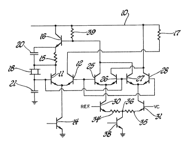
Referrin~ to Figure 1, a voltage supply rail
10 is connected to an electric power supply, not shown,
capable of supplying current on demand at a
predetermined supply voltage. A first differentially
connected pair of transistors comprises transistors 11,
12 having emitters coupled together and, through a
current source transistor 14, to the ground of the
power supply. All transistors in this circuit are
shown as NPN, bipolar transistors for illustration only
and are not to be restricted thereto; those s~illed in
the art will be able to construct embodiments of the
~ invention using a variety of transistor types and
polarities. In addition, for each of the
differentially connected transistor pairs having
coupled emitters, the control terminals are bases and
the output terminals are collectors. Different types
or polarities of transistors might have different names
for their control and output terminals without
departing from this invention.
The output terminal, or collector, of
3~1
transistor 11 is connected to supply rail 10, in
series, through a load resistor 15 and the emitter and
collector of a transistor 16. Likewise, the collector
of transistor 12 is connected to supply rail 10 throu~h
a load resistor 17. A cr~stal 18 is connected in a
feedback loop from the collector of transistor 11 to
its base. A capacitor 20 is connected from the
collector of transitor 11 to the emitter of transistor
16, in parallel with resistor 15; and a capacitor 21 is
connected from the base of transistor 11 to ground.
Crystal 18 and capacitors 20, 21 thus form a pi network
in the feedback loop around transistor 11.
A second pair of differentially connected
transistors 25, 26 has coupled emitters connected to
the collector of a transistor 30. Likewise, a third
differentially connected pair of transistors 27, 28
has coupled emitters connected to the collector of a
transistor 3t. Transistors 30, 31 form a fourth
differentially coupled pair having emitters connected
through a pair of resistors 34, 35 in series. The
junction 36 of resistors 34 and 35 is connected through
a transistor 38 to ground. The collectors of
transistors 26 and 28 are connected to supply rail 10,
~ and the collectors of transistors 25 and 27 are
connected to the base of transistor 16 and also through
a resistor 39 to supply rail 10. The bases o~
transistors 26 and 27 are coupled to the base of
transistor 11, and the bases of transistors 25 and 28
are coupled to the base of transistor 12. ~lements
25-38 thus form a balanced modulator which applies an
output voltage through transistor 16 to the feedback
loop at capacitor 20. There are means, not shown, for
1;~7~81
generating a constant reference voltage REF and
applying it to the base or control terminal of
transistor 30. Likewise, there are means, not shown~
for generating a control voltage and applying it to the
base or control terminal of transistor 31. The control
volta~e VC is a DC voltage but is variable in voltage
level to control the output of the balanced modulator.
Transistor 38 is a current source for the balanced
modulator, which may be switched on and off by the
voltage applied to its base to activate and deactivate
the balanced modulator.
To provide for operation as a free running
crystal oscillator, the voltage at the base of
transistor 38 is set low to turn ofE the balanced
modulator 25-38. The pi network 18-21 in the feedback
loop around transistor 11 qenerates a 180 degree phase
shift at a predetermined frequency which, when added to
the 180 degree phase shift from base to collector of
transistor 11, creates positive reinforcing feedback to
produce oscillation of the amplifier comprising
transistors 11, 12 at the predetermined frequency. In
this mode of operation, the oscillator is a standard
crystal contolled, phase shift oscillator; and provides
the stable and predictable operation associated with
such oscillators~ It is, in particular 7 not subject to
variations of a control volta~e or of additional phase
shift networks.
To vary the frequency of operation of the
oscillator from the predetermined frequency, transistor
38 is turned on by providing an appropriate DC voltage
on its base. This activates the balanced modulator
25-38 which, since it is coupled to the bases of
., - : .
1'~79~38~
transistors 11, 12, generates an output voltage varying
at the same fre~uency as the frequency of oscillation
of amplifier 11, 12. The amplitude and phase of this
output, however, vary with the control voltage VC
applied to the base of transistor 31, relative to the
reference voltage REF applied to the base of transistor
30. If the control and reference voltages are e~ual,
the amplitude of the output is zero. As control
voltage VC varies in one direction from the value of
reference voltage REF, the amplitude of the output
increases in phase with the output of differential
amplifier 11, 12. As control voltage VC varies in the
opposite direction from the value of reference voltage
REF, the amplitude of the output also in~reases, but
180 de~rees out of phase with the output of
differential amplifier 11, 12.
The output of balanced modulator 25-38 is
applied through the emitter of transistor 16 to
capacitor 20. The emitter of transistor 16 is, at high
2Q frequencies typical of the operation of the oscillator,
at ground potentialO The pi network 18-21 can thus be
shown as the e~uivalent circuit of Figure 2, with the
output of transitor 11 applied at the terminal labelled
~ "AMP SIGNAL IN" and the modulator signal applied at the
terminal labelled "MODULATOR SIGNAL IN". The modulator
signal is thus 90 degrees out of phase with the output
of transistor 11, due to capacitor 20, as the two are
combined. The resusltant feedback signal may be
understood with reference to the phasor diagram of
Figure 3~ I~ the output of balanced modulator 25-38
has zero amplitude, the feedback signal will be
essentially unaffected thereby and the result will be
~7~38~
as shown in phasor 50, which represents a phase shift
of 180 deqrees. If the balnced modulator signal
increases in amplitude due to control voltage VC
varying in a first direction from reference voltage
REF, it will produce the phasor 51. The resusltant
phasor 52 will have a phase angle differing from 180
degrees in one directionO Thus, in order for
oscillation to take place, the oscillator will have to
shift its frequency of oscillation in a first direction
from the predetermined freauency to the fre~uency at
which the crystal shifts the phase back to 180 degrees.
Likewise, if control voltage VC varies in the opposite
direction from the reference voltage REF, the amplitude
of the balanced modulator output will increase in the
opposite phase to generate phasor 53. The resultant
phasor 5~ will cause a variation in frequency of
oscillation in the opposite direction from the
predetermined frequency. Clearly, the phasors shown
are only examples - a continuous range of frequency
ad~ustment is possible in both directions from the
predetermined frequency.
.