Note: Descriptions are shown in the official language in which they were submitted.
~L27~39C)~9
DESCRIPTION
AMPLITUDE MODULATED ~ROADCAST TRANSMITTER
Technical field
The invent;on relates to the field of broadcast
engineering. In particular, it concerns amplitude modu-
lated broadcast transmitters (AM broadcàst transmitters)
having
- an RF output stage which is equ;pped with at
least one output stage tube;
- a main modulator in the form o~ a switching am-
plifier uhich outputs an anode volt3ge, modulated as deter-
mined by an LF input signal, to the output stage tube; and
- a radio frequency circu;t with a carrier frequen-
cy source for generat;ng a Garrier s;gnal and a sub-
sequent driver stage which amplifies the carrier signal
and passes it to a control grid of the output stage
tube.
Prior art
In amplitude modulated h;gh power broadcast trans-
mitters, for example short or medium wave transmitters
of several 100 kW transmitting power, the achievable ef-
fic;ency is of great importance for the operating costs.
In particular, the construction and the mode of operation
of the modulator used has a decisive significance for the
efficiency.
The latest policy has therefore been to replace
the class 8 push-pull modulator equipped with two high
power tubes normally used until n~w with a semiconductor-
equipped sw;tching amplifier which either operates with
pul~e duration modulation (P~M) (see, for example, EP-~1
0 Q25 234) or is constructed as socalled pulse step mod-
ulator (PSM) (see, for example, ~rown Bover; Review 5
(1985), pages 235-24û).
114/86
~'7~
Z
In both cases, the power amplification of the LF
input signal necessary for the modulation is no longer
performed by means of a linear amplifier but by means of
a time-controlled switching on and off of switching
stages with an output voltage which remains the same.
The amplified analog signal is then recovered by means of
a lowpass filter located at the output of the switch;ng
amplifier.
In the case of the PDM modulator, the duration-
modulated pulses cannot become shorter than a minimumpulse duration due to the fin;te switching times of
the switching elements used (for example thyristors~.
The result is that, when the modulat;on is actually 100 %
(m = 1), the required zero value of the RF output power can-
not be ach;eved at minimum modulation, that is to say atthe minimum of the LF input signal, because the switch;ng
amplif;er outputs a minimum modulation power to the RF
output stage below which it cannot go. 100 % full modu-
lat;on can therefore not be achieved with this type of
modulator.
The same cons;derations also apply to the PSM
modulator because, in addition to the coarse stairstep-
like approximation of the required output voltage vari-
ation by the (for example 32) switching stages, a fine
approximation is also performed ~ith the aid of a super-
imposed pulse duration modulation.
Representation of the invention
The present invention then has the object of cre-
ating an amplitude modulated broadcast transmitter which
exhibits the advantages which can be achieved by means of
a modulator constructed as switching amplif;er and, at
the same t;me, can be fully modulated at 100 %.
In an AM broadcast transmitter of the type ini-
tially mentioned, the object is ach;eved by the fact
that, in order to real;~e up to 100 % modulation, even at
the modulation minima, means are provided by means of
114/86
~7~7
-- 3
which the zero value of the RF output voltage output by
the RF output stage can be con~inuously attained at a
modulation minimum via control of the carr;er signal as
determined by the LF input signal.
Thus, the core of the invention consists in modu-
lating, in addition to the known modulation of the anode
voltage for the output stage tube, also the carr;er sig-
nal at modulation minima with approximately 100 ~ modu-
lation in order to continuously set by this means the
zero value of the RF output voltage via the control grid
of the output stage tube.
This additional modulation of the carrier signal
is preferably performed by means of an additional modu-
lator which is disposed in the radio frequency circuit
immediately behind the carrier frequency source.
In this arrangement, the LF input signal neces-
sary for controlling the additional modulator is picked
up, in particular, directly at the input of the main mod-
ulator and applied to the additional modulator via a
delay circuit which delay circuit compensates for the
signal trans;t time in the main modulator.
It is also particularly advantageous to dispose
between the delay circuit and the additional modulator a
correction circuit which, in particular, compensates for
nonlinearities of the RF output stage and of the addi-
tional modulator and predetermines a starting point for
the additional modulation of the carrier signal in the
additional modulator, from which this modulat;on starts.
These and other illustrative embodiments are
found in the subclaims.
~rief description of the drawings
In the text which follows, the ;nvention will be
described and explained in greater detail with the aid of
illustrative embodiments, in conjunction with the draw-
ing, in which:
Figure 1 shows the basic conf;gurat;on of a known
114/86
9~
-- 4 -
PSM modulator;
Figure 2 shows the output voltage of a modulator
according ~o Figure 1, with stairstep- like approximation
of an ;llustrative signal variation;
Figure 3 shows a diagram of the pulse duration
modulat;on ;n a switching ampl;f;er,
F;gure 4 shows an ;llustrat;ve modulated RF out-
put voltage with modulat;on minimum;
F;gure 5 shows a block d;agram o~ a preferred em-
bodiment of the broadcast transmitter according to the
invent;on;
Figure 6 shows a detailed c;rcu;t of a successful
embodiment of the add;tional modulator and of the correc-
tion circuit accord;ng to F;gure 5; and
F;gure 7 shows a detailed circ~;t of a successful
embodiment of the delay circuit according to Figure 5.
Approaches to carrying out the invention
The e~planations following are based on the exam-
ple of a broadcast transm;tter with PSM modulator without
restriction of the generality.
The basic circuit diagram of such a PSM modu-
lator, as ;t is known from the printed document Brown
80veri Rev;ew initially mentioned, is shoun in F;gure 1.
The central part of the modulator is a switching ampli-
fier consisting of a plural;ty of similar switch;ng
stages 7.
Each sw;tch;ng stage 7 has an approximately con-
stant output voltage Us which determines the he;ght of thesta;rsteps ;n the approximation of a steady signal vari-
ation (Figure 2). To generate this output voltage US,
each switching stage 7 is connected to a separate secon-
dary winding of a power system transformer 1, the primary
of ~hich is operated, for example, across a medium vol-
tage system (3 ... 24 kV).
The alternat;ng voltage of each secondary coil is
rectified in each switching stage by means of a rectifier
- 114/86
3~
-- 5
8 and smoothed by a combination of smooth;ng choke 9
and capacitor bank ~. The switching stages 7 can be suc-
cessively connected in series or disconnected from the
series circuit by corresponding change-over s~itches 3 at
their output.
The change-over switches 3 are controlled as de-
termined by an LF input signal present at an LF ;nput 10 by
a switch;ng stage control system 4 via potential-
isolating optical wave guides 5.
The summed output voltages Us Of the series-
connected switching stages 7 are supplied to a lowpass
filter 6 through which the steady analog signal is re-
covered in amplified form. The stairstep-Like voltage
before and the smooth output voltage UA after the lowpass
filter 6 are shown together in Figure 2 in an illus-
trative curve trace. The output voltage UA here fluc-
tuates around a mean value of 14 kV.
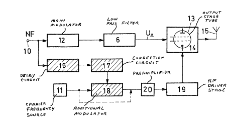
In a broadcast transmitter of known type, the
block diagram of which can be seen in Figure 5 if the
function blocks drawn shaded in this figure are omitted,
the switching amplifier according to Figure 1 is used as
main modulator 12 with the subsequent lowpass filter S.
The output voltage UA is used as modulated anode voltage
for an output stage tube 13, in most cases a high power
tetrode, used in the subsequent RF output stage 14. -
The carrier frequency, the amplitude of which isto be modulated with the LF input signal, originates from
a carrier frequency source 11, an oscillator or frequency
synthesizer. The carrier signal from the carrier fre-
quency source 11 is amplified tpassing along the pathdrawn ~ith a dashed line) in a preamplifier 20 and an RF
driver stage 19 and then applied to a control grid of
the output stage tube 13 in the RF output stage 14.
The preamplifier 20 is ;n rnost cases a wideband
transistor amplifier and the Rf driver stage is frequent-
ly equipped with a driver tube. Together with the car-
rier frequency source 11 and the RF output stage 14, they
form a rad;o frequency circuit the more detailed
114/86
'7~3~)
-- 6
construction of which can be seen, for example, ;n the
printed document Brown Boveri Review 5/6 (1983), pages
235 - 240.
As has already been mentioned, the relatively low
S number of switching stages in the switching amplifier
(for example 32) means that a fine approximation of the
steady signal must be prov;ded by additional pulse dur-
ation modulation in order to achieve a smoother curve
variation. At least one of the switching stages in the
series circuit therefore outputs the pulses shoun in Fig-
ure 3, having the period T and variable pulse duration
(indicated by the dual arrow). In this pulse duration
modulation mode, the pulse duration cannot drop below the
minimum pulse duration drawn shaded because of the finite
switching times of the switching elements used.
This means that, differently from the ideal;zed
case shown in Figure Z, the value UA = ~ cannot be con-
tinuously achieved at a modulation minimum with 100 %
modulation. On the output side of the transmitter, at
the antenna 15, there is therefore a signal according to
Figure 4 present in which the carrier frequency TF ex-
h;b;ts an envelope E which does not follow the curve
(drawn with a dashed line) for 100 ~ modulation at the
minimum but only assumes a finite minimum value Em.
Since such a curve variat;on, however~ is equivalent to
additional distortion, 100 % full modulation could not,
therefore, be used ;n transmitters of the prior art and
the modulation could only extend to a percentage at which
the minimum value Em of the envelope was reached in each
case at the modulation minima.
In order to be able to retain the main modulator
12 in the form of the switching amplifier unchan~ed with
all its advantages and, nevertheless, provide the possi-
bil;ty of steady 100 % full modulation, the carrier sig-
nal is additionally modulated in the radio frequency cir-
cuit, that is to say greatly reduced~ at the critical
points of the modulation minima when the minimum value Em
of the envelope is reached, according to the invent;on.
114/86
~27~
-- 7
The RF output signal can be further reduced in this man-
ner at the modulation minimum via the control grid of the
output stage tube 13 even though the anode voltage Uh re-
mains constant at its minimum value. The combined modu-
S lation via the anode voltage and the carrier s;gnal thusallows 100 % modulation ~ithout any disadvantages.
In the preferred embodiment of the ;nvention ac-
cording to Figure 5, an additional modulator 18 is in-
serted into the radio frequency circuit immediately be-
hind the carrier frequency source 11 (the dashed line hasno significance in this case) for the additional modulation
of the carrier signal.
The LF signal needed for controlling the addi-
tional modulator 18 is picked up directly at the input of
the main modulator 12, that is to say after the input
filters which may be present at the LF input 10. Since
the main modulator 12 has a relatively long signal tran-
sit time but the two modulations must occur matched to
each other in time, a delay circuit 16 must first be in-
serted before the additional modulator 18 ~hich compen-
sates for the signal transit time caused by the main mod-
ulator 12, particularly at higher modulation frequencies.
In addition to the delay in the delay c;rcuit 16,
the LF signal must be precorrected in a correction cir-
cuit 17, for the following reasons:- nonlinearity of the RF output stage 14
- nonlinearity of the additional modulator 18
- starting point of the additional modulation only
in the region of high modulation
- minimum influence on I91 of the output stage
tube 13
- no additional spurious radiation in thq RF
spectrum.
The detailed circuits of successful embodiments
of the additional modulator 18 and of the correction cir-
cuit 17 are shown in Figure 6.
The actual additional modulator 18 consists of a
two-stage controllable attenuator with the dual field
114/86
-- 8
effect transistor T3, T4 followed by an impedance con-
verter with the transistor T5 in order to avoid any un-
specifiable loading of the attenuator by the subsequent
preamplifier 2~.
The correction circuit 17 is constructed as non-
linear amplifier with the operational amplifiers V1 to
V4~ For the above reasons~ only relatively narrow negative
peaks are needed for the additional modulation of the
carrier signal, but without any irregular transitions.
1 0 Assuming a sinusoidal modulation signal ~see, for
example, Figure 4), the upper portion of the sine wave is
severely compressed by the nonlinear resistance of the
diodes D5 to D8.
The shape of the negative peaks can be influenced
1 5 by an addition of even narrower sinusoidal peaks which
are obtained by the diodes D1, D2 and the operational am-
plifier V2 and the amplitude of which can be adjusted by
means of the potentiometer P3 in order to achieve an im-
provement in the total harmonic distortion with 100
2 0 modulation.
The transistors T1 and T2 and the LEDs form an
indicating circuit. The LED is illuminated when 100 ~
modulation is reached, driven by a monostable flip flop
formed by the transistors T1 and T2 with a sufficiently
2 5 long conduction period at each modulation peak. This in-
dicating circuit is mainly used as adjustment aid.
The potentiometer P1 is used for setting the LF
input level and the potentiometer P2 is used for setting
the required starting point. Matching the modulation
3 û characteristic of the transistors T3, T4 and thus the re-
quired shape of the envelope is then achieved by means of
potentiometers P4 and P5.
The additional modulator 18 has a frequency range of
up to 30 MHz.
3 5 The detailed circuit of a successful embodiment
of the delay circuit 16 is shown in Figure 7. Since a
traditional delay line for the required delay times and
the LF range is too expensive, the delay circult of Figure
114t86
~'79~
7 is constructed as three-stage active lowpass f;lter
combined with an adjustable all-pass filter.
These 3 stages of the lowpass filter are imple-
mented by means of the operational amplifiers V5 to V7.
S The potentiometer P6 can be used for correcting, as required,
the amplitude characteristic at higher frequencies and the
potentiometer P7 is used for setting the coincidence between
main and additional modulator at about 4 kHz.
The delay circuit according to Figure 7 results
1û in the required delay in the frequency range from 50 Hz
to 5 kHz.
Commercially available components of su;table
size can be used for the operational amplifiers V1, ....
V8, the transistors T1, ~.., T6, the diodes D1, ..., D8,
the resistors R1, ..., R42, the capacitors C1, ..., C23
and the potentiometers P1, ..., P7 of the circuits of
Figures 6 and 7.
Overall, the invention results in an AM broadcast
transmitter which exhibits the advantages of modulation
by means of a switching amplifier and, at the same time,
can be fully and continuously modulated up to 1ûO %.