Note: Descriptions are shown in the official language in which they were submitted.
NE-181~l2~7~91906
TL~ OF THE INVENTION
2 "CARRIER RECOYERY CIRCUIT F'OR OFFSET QPSK
3 DEMODULATORS"
4 BAC~CGROUND OF THE INVENTION
S The present inven~ion relates generally to a camer recovery circui$
6 for an offset QPSK (quadrature phase shift keying) demodulator.
7 Offset QPSK is a form of QPSK in which the digits in the quadrature
8 channels have a relative delay in their transitions. If the serial input data
9 have symbol duration T, then the I and Q data will each have symbol
duration 2T. The relative delay between channels is T. In conventional
1 1 QPSK the transitions are coincident The purpose of thls delay is to restrict
12 the carrier phase transitions from having 180 phase transitions. When
l 3 filtered, the o~fset QPSK will have less envelope fluctuation compared
14 with QPSK In the unfiltered case, the introduction of a delay has no
15 performance effect and offset QPSK has the same error rate as does
l 6 conventional QPSK As is well known, signals are transmitted in the form
17 of a succession of shor~-duration bursts in satellite communications system
l 8 for minimizing satellite's power consumption and for enabling time
1 9 division multiple access. In order to ~educe demodulator signal acquisition
2 0 time, bursts are structured so that each starts with a preamble containing
2 l bits that accentuate carrier and clock frequency spectra. The preamble for
2 2 each o~ the quadrature channels begins with a carrier recovery field which
23 is followed by a cloclc recovery field. Specifically, the carrier recovery
2 4 fields of both of the quadrature channels contain a successian of all binary25 1's. Whereas the clock recovery field of in-phase channel contains a
2 6 succession of all binary 1's as in the carrier recovery field and the clock
NE-1 81 ~L~7
recovery field of the quadrature channel cs~ntains a succession of
2 alternating binary 1's and binary 0's. Since demodulators of satellite
3 transmission systems operate at low carrier-to-noise (C/N) ratios and
4 since the preamble is of a short duration for channel utilization efficiency,
S it can occur that demodulators fail to successfully recover a carrier at the
6 end of the carrier recovery field and hence the recovered carrier still
7 contains a phase error at the beginning of the clock recovery field. This
8 implies that carrier recovery action should con~inue after entering the clock
9 recovery field. However, with conventional carrier recovery circuits for
10 offset QPSK demodulation, clock timing is not successfully recovered at the
11 beginning of the clock recovery field. Even though a delay has been
12 introduced in a Costas loop with a view toward coinciding phase
13 transitions between in-phase and quadrature channels, it is impossible to
14 continue to the carrier recovelg process in the clock recovery field.
SUMMARY OF THE INV~NIIC)N
l 6 It is therefore an object of the present invention to provide a carrier
l 7 recovery circuit for an offset QPSK demodulator which permits carrier
l 8 recovery process to continue in a subsequent clock recove~y field.
19 The signal received by the carrier recovery circuit an offset QPSK
20 modulated signal having first and second channels of quadrature phase
2 l relationship. Each of said channels has a carrier recovery field and a bit
22 timing recovery field (BTR~, the carrier recovery field of each of said
2 3 channels and the BTR of the first channel having a series of binary digits of
2 4 identical logic values and the Bll~ of said second channel having a series of
2 5 binary digits of alternating logic values.
26 According to the present invention, the carrier recovery circuit
NE-181 1~79~3~D6
comprises a voltag~controlled oscillator with a ~/2 phase shifter coupled
2 to it for generating carriers of quadrature phase relationship, first and
3 second phase comparators ~or detecting phase differences between the
4 first and second channels of the offset QPSK modulated signal and the
S carriers of the quadrature phase relationship. Si~nal from one of these
6 phase comparators is delayed by a 1/2 symbol duration and applied to one
7 input of a quadri-phase detector having stable phase angles at 7514, (3/4)7~,
8 (5/4)~ and (7/4)~ radian and signal from the other phase comparator is
9 applied to the other input of the quadri-phase detector. A bit timin~
10 recovery field (BT~) detector is connected to the second phase comparator
11 for detecting a BTR of the second channel. Signal from the quadri-phase
12 detector is applied to a loop filter and thence to the voltage controlled
13 oscillator when a E~TR of the second channel is not detected by the BTR
14 detector. In response to the detection of a Bll~ of the second channel, the
15 output of the second phase comparator from which that Bll~ is detected is
16 briefly switched to the loop filter, instead of the signal from the quadri-
17 phase detector.
18 This switching operation stabilizes the operation of a carrier
19 recovering closed loop of the circuit against the effect of a phase error
2 0 which occurs as a result of an unsuccessful recove~y of caITier from a clock21 recovery field, allowing the carrier recovery process to continue in a
2 2 succeeding clock recovery, or bit timing recovery field.
2 3 In a preferred embodiment, an envelope detector is connected to the
24 outputs of the first and second comparators for detecting the carrier
2 5 recovery field of at least one of the first and second channels. Initial phase
2 6 error of a closed loop formed by the carrier recovery circuit with respect to
NE-181 ~ 799~
a signal phase of the offset Qr'SK signal is estimated from the outputs of
2 the first and second phase comparators. Frequens~y offset of the carriers is
3 estimated from the initial phase error. A variable phase shiff er is provided
4 for introducing a constant phase shift of (7~/4) radian and a variable
S arnount of phase shift equal to the es~imated initial phase error to the
6 carriers when a Glrrier recovely field is detected by the envelope detector.
7 Signal from the second phase comparator is combined with the frequency
8 offset and applied to the VCO as a frequency control signal when the
g carrier recovery field is not detected by the envelope detector. When the
10 carrier recovery field is detected by the envelope detector, signal from the
1 1 loop filter is combined with the ~requency offset, instead of the signal from
12 the second phase comparator, and applied to the YCO as the frequency
l 3 control signal.
14 BRIEF DliSCRIPIION ~:)F THE DRAWINGS
1 S The present invention will be described in further detail with referenc
16 to the accompanying drawings, in which:
17 Fig. 1 is a block diagram of a carrier recovery circuit according to one
18 embodiment of the present invention;
19 Fig. 2 is a timing diagram useful for describing the operation of the
2 0 Fig. 1 embodiment;
21 Fig. 3 is a block diagram of a carrier recovery circu;t of a preferred
2 2 embodiment;
2 3 Fig. 4 is a circuit diagram of an envelope detector of Pig. 3; and
24 Fig. 5 is a timing diagram and scattering diagrams associated wi~h
2 5 the embodiment of Fig. 3.
,i
,~ ~
NE-181
DETAILED DES(:P~IPTION
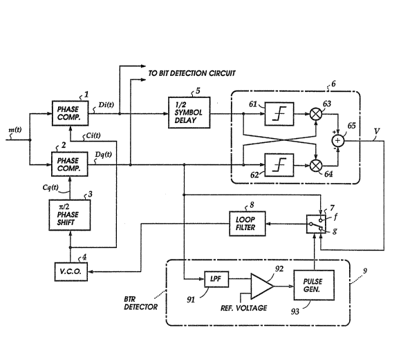
2 Referring now to Fig. 1, there is shown a carrier recovery circuit of
3 an offset QPSK demodulator according to a preferred embadiment of this
4 invention. An IF (intermedia~e frequency) offset ~2PSK input si~nal m(t),
S which contains an in-phase channel component I(t) and a quadrature
6 channel component Q(t), is applied to an in-phase charmel phase
7 comparator 1 and a quadrature channel phase comparator 2, where the
8 offset QPSK signal is represented as:
9 m(t) = 2 I(t) (ej~ct + e-j~ct) + 21j Q(t) (ei~Dct + ej~ct) ~1)
Phase comparators 1 and 2 each multiply the input QPSK signal with
11 quadrature versions Ci(t) and Cq(t) of a recovered carrier which are
12 respectively supplied from the output of a voltage-controlled oscillator 4
13 via a ~witch 13 and the output of a 7ç/2 phase shifter 3 which introduces a
14 ~/2 phase delay to the output of VCO 4. The output of phase ~omparator 1
1 5 is applied to a 1/2 symbol delay circuit 5 as a phase differenoe between the16 in-phase channel signal Di(t) and one of the carriers and thereafter to one
17 input of a quadri-phase comparator 6 and the output of phase comparator
18 2 is applied to the other input of the quadri-phase detector 6 as a phase
19 difference between the quadrature channel signal Dq(t) and the other
2 0 carrier. The outputs of phase comparators 1 and 2 are further applied to a
21 bit detection circuit, not shown.
2 2 Since the recovered quadrature carriers can be represented by:
2 3 Cj(t) = ei(~ct + ~) + e-j{~ct + ~) (2)
2 4 Cq(t) = Jl lei(oct + ~ + e-j(a~ct + ~)] (3)
2 5 where a represents the phase error of the recovered carrier, the detected
2 6 quadrature baseband signals are represented by:
NE-181
- 6 -
Di(t) = m(t) Ci(t)
2 ~ 2 I(t) [ej~ ~ ej~] + ~Q(t) [e~~ ] (a
3 Dq(t) = m(t) Cq(t)
4 ~ 2j I(t) [ej~- ej~] + ~(t) 1e~0 + e j~] (5~
S Since the carrier and cloclc recovery fields of the I-channel signal
6 contain all binary 1's, they can be rep~esented by:
7 I(t~= 1 (6)
8 Substiblting it into Eguations 4 and 5, the following relatior s hold:
9 ~i = cos ~ - Q(t) sin ~
l O Dq = sin ~ ~ Q~t) cos ~ (8)
1 1 The purpose of the 1/2 symbol delay circuit 5 is to coincide the phase
1 2 transitions between the I and Q channels. The 1/2 symbol delay pr~duces
1 3 an output signal Dq which is given b~r.
14 Dq=Dq(t~ 2)-sin~Q(t+ 2)cos~ (93
The quadri-phase detector 6 is of a conventional design and includes
16 a pair of data detectors 61 and 62 to which the I- and ~channel signals are
17 respectively applied, and a pair of multipliers 63 and 64 connected
18 respectively to the outputs of data detectors 61 and 62. Each multiplier
19 multiplies the output of associated data detector with the input of the data
20 detector of the other channel. The outputs of multipliers 63 and 64 are
2 l subtracted from each other by means of a subtractor 65. As is well known,
~2 the quadri-phase detector 6 has ~our stable points, namely, ~l4, (3/4)~,
2 3 (5/4)~ and (7/4)~ radian. Assume that the phaæ error ~ is much smaller
2 4 than unity, the outputs of the data detectors 61 and 62 are given as follows:
SGN (Dj~ = SGN (cos ~) ~ 1 (10)
~7
NE-181
- 7 -
SGN (~) = SGN ~sin ~ -~ Q(t ~ 2 ) cos û~
2 ~ SGN (sin ~ + Q(t ~ ~ )) S11)
3 where, ~N (-) denotes the signum function.
4 As a Tesult, the output sig~l V of th~ quadri-phase detector 6 i~ given
S by the following Equati~n:
6 V = SGN(Di) Dq- SGN( Dq~ DI
7 - sin a ~ Q(t + 2 ) - SGN (sin ~ ~ Q(t + 2 )) (12)
8 The output of quadri-phase comparator 6 is applied to a position g s: f
9 a switch 7 and thenoe to a loop ~ilter 8 whose output is supp]ied as a control
10 signal to the VC~ 4, completing a Costas loop. If clock timing is
11 successfully established during the clock recovery field, then the relation
12 Q(t) = + 1 holds. Hence the second and third tenns of ~quation 12 become
l 3 equal to each other and the following relation holds:
14 V~ sin ~ (13)
In this way, the phase error ~ of the recovered carrier can be de~ved
16 from the output of the quadri-phase detector 6. This implies that even
l 7 though a carrier has not been successfully recovered at ~he beginning of the
18 clock recovery field, a successful recovery of clock timing at the ~ginning
19 of the clock recoveIy field allows the carrier recovery process to continue
2 0 during the clock recovery field to complete a carrier recovery process.
~1 In the prior art demodulatvr, however, the cloclc timin~ is not
2 2 sucoessfully recovered at the beginning of the clock recovery field aIId the
2 3 second and third terms of Equation 12 may exist a phase error component.
24 This phase error component of the output of quadri-phase detector 6 is
2 5 passed through the loop filter 8 to the VCO 4 as a control signal, causing
2 6 the prior art phase lock loop to go out of phase with the input signaL This
,~,,
NE-181
is the r~ason why the use of a 1/2 symbol delay circuit in the prior art offset
2 QPSK demodulator is not suffldent for successful carrier recovery.
3 According to the present invention, the switch 7 is provided for
4 selectively coupling the Dq(t) output of the ~channel phase comparator 2
S and the output V of quadri-phase detector 6 to the loop filter 8, and a BTR
6 (bit timin~ recovery field) detector 9 for d~ecting the bit timing recovery
7 field of the ~channel signal from the output of phase comparator 2.
8 Switch 7 normally connects its contact arm to the contact position g in the
9 absence of a control signal from the BTR detector 9 and switches its contact
1 Q arm to the contac~ positis:)n f in response to that control signal.
11 BTR detector 9 comprises a low-pass filter 91 for filtering the output
12 of phase comparator 2, a comparator 92 for comparing the filtered Q-
13 channel signal with a reference voltage arld a pulse generator 93. When a
14 carrier recovery field of the ~ehannel is detected by phase comparator 2,
15 the low-pass filter 91 is charged by a series of all binary 1's of that carrier
16 recovery field, developing a voltage which exceeds the reference voltage
17 and producing a high level output from the comparator 92 as shown in Fig.
18 2. When the bit timing recovery field of the Q channel is subsequently
19 arrived, the voltage at the output of low-pass filter 91 decreases below the
2 0 reference voltage as it discharges its energy in response to the alternating
21 binary 1's and O's of the t~channel bit timing recovery field. The output of
2 2 comparator 92 switches to a low voltage level indicating the detection of a
2 3 BTR and the pulse generator 93 supplies a control pulse to the switch 7 to
24 briefly couple the output of ~channel phase comparator 2 to the loop
2 5 filter 8 instead of the output of quadri-phase detector 6.
2 6 As a result, the loop filter 8 now filters an alternatin~ series of binary
799~6
NE-181
l's and O's when a bit timing recovery field of the Q-channel signal is
2 detected by the BTR detector 9. This implies that the second term of
3 Equation 8 is nulli~ied by the l~op filter 8 and so its output reduces to a low
4 level indicatirlg a phase error of the recovered carrier. The control pulse
S applied to the switch 7 continues for a duration sufflcient to reduce the
6 phase error to æro.
7 A preferred form of the carrier recovery circuit is showII in Fig. 3.
8 This embodiment comp~ses an envelope de~ector 11 which receives inputs
9 from the I- and ~channel phase comparators 1 and 2 by way of IDW PaSS
10 filters 17 and 18 and supplies an output to switches 13 and 15. A variable
1 1 phase shifter 1~ is provided, which is connected to the output of VCO 4 to
12 introduce a delay in accordance with the output of an initial phase error
13 estimator 19. The output of variable phase shifter 12 is connected to the k
14 contact position of switch 13. The output of VCO is also applied to the j
15 contact position of switch 13, the contact arm of switch 13 being connected
16 to phase comparator 1 and ~;/2 phase shifter 3. Initial phase error
17 estimator 19 derives its inputs from low-pass filters 17 and 18 to generate a
18 signal representative of an initial phase error ~e which is generated in the
19 recovered carrier at the beginning of carrier recovery fields of the I- and
2 0 ~ehannel signals due to frequency offset ~f of ~he carrier in the first order
21 loop. The initial phase e~or estimator 19 estimates the phase error ~e by
2 2 calculating Equation 14:
2 3 ~e = tan I ~Di (t)/Dq'(t)} = 2~f/k (14)
2 4 where k is the loop gain of the Costas loop and Di'(t) and Dq'(t) represent
25 the outputs of low-pass filters lY and 18, respectively, and are given as
2 6 follows:
~L~t7~
NE-181
- 10 -
~'(t) = A cos (2~c~f/k~ tl5)
2 Dq'(t) - A sin (2~f/k) (16)
3 ~f = 27c ~e (17)
4 The output of phase error estin~tor 19 is also applied to a frequency
S offset estimator 14 which estimates the frequency offset ~f by calculating
6 Equation 17 and dividing ~f by a factor equal to the gain kVCo of VCO 4 to
7 derive a VCO control voltage Vf = (k/kVCo 27~) ~e ~or application to VCO 4
8 by way of an adder 16 ~o which the output of switch 15 is also applied.
9 As shown in Fig. 4, the envelope detector 11 comprises a pair of
10 squaring circuits 191 and 192 coN~ec~ed respectively to low-pass filters 17
11 and 18. The outputs of squaring circuits 191 and 192 are summed by an
12 adder 193 and applied to a comparator 194 for comparison with a
13 reference Yoltage, the output of the comparator 194 being supplied to the
14 switches 13 and 15.
The operation of the CR detector of ~ig. 3 will be described with
16 reference to Fig. 5. During the time prior to the reception of an offset
17 QPSK signal, switches 7. 13 and 15 are switched to their g, j and h contact
18 positions, respectively, and the Costas loop operates in the mode of first-
19 order phase locked loop. On receiving the carrier recoveIy fields of botch
2 0 channels of the QPSK signal, the Costas loop is quicldy phased locked in a
21 manner characteristic of the first-order PLL. Because of all binary 1'5 of
22 the carrier recovery fields, the squaring circuits 191, 192 of envelope
2 3 estimator 19 both generate high level outputs and the sum of thes~e outputs
2 4 exceeds the reference Yoltage of comparator 194. Thus, switches 13 and 15
2 5 are moved to their k and i positions, respectively, coupling the output of
2 6 loop ilter 8 to the adder 16 and the ou~put of variable phase shifter 12 to
NE-181
the phase compara~ors 1 and 2. A signal represezl~ative of the ini~ial phase
2 error 0e is derived and supplied from ~he phase error estimator 19 to
3 frequency offset estimator 14 which, in turn, derives a VCO control voltage
4 Vf, which is applied through adder 16 to the VCO 4. Variable phase shifter
5 12 is also supplied with the initial phase error to delay the phase of the
6 VCO 4 output by an amount equal ~ (4 - 0e3 When the switch 13 ~s moved
7 to the i position, the quadri-phase detector 6 enters the quadri-phase
8 mode, leaving the single-phase mode. BetYveen these stable points there is
g a phase difference o ~/4 radian. However, by virtue of variable phase
10 shifter 12, this phase difference is compensated.
1 1 The lower part of Fig. 5 illustrates scattering diagrams in the cases of
l 2 three successive modes having zero frequency error and in the cases of
13 corresponding modes in which frequency error exists. It is seeII that
14 regardless of whether there is a frequency error or not, the phase
1 5 difference of ~/4 radian is compensated for when the switch 13 is moved to
l 6 the i position. In the presence of a frequency error ~f, the resulting initial
l 7 phase error ~e is compensated for by virtue of the frequency offset
l 8 estirnator 14.
l 9 Since the output of the envelope detector 11 corresponds to the
2 O output of comparator 92 of Fig. 1, it can be used as an input signal for a
21 pulse generator 10 to generate a switching pulse of the switch 7.
2 2 Subsequent to the detection of a CR field. the pulse generator 10 generates
2 3 a pulse in the presence of a BTR field of the ~channel signal to move the
2 4 switch 7 to the f position for a brief interval, coupling the output of quadri-
2 5 phase detector 6 to the loop filter 8. The output of loop filter 8 is applied
26 through switch 15 to adder 16 where it is summed with the output of
NE-181
- 12-
frequency offset estimator 14 and applied to the VCO 4 as a frequency
2 control signal.
3 The foregoing des~ption shows only pr~ferred embodiments of
4 the present invention. Various modifications are apparent to those
S skilled in the art without departing from the scope of the present
6 invention which is only limited by the appended claims. Therefore, the
7 embodiments shown and described are only illustrative, not
8 restrictive.