Note: Descriptions are shown in the official language in which they were submitted.
~'~80~4(~
- l - 41PS 6372
LOW VOLTAGE VAC[JUM CIRCUIT INTERRUPTER
BACRGROUND OF THE INVENTION
The provision of a solid state switch across
a pair of separable contacts to reduce arcing between
the contacts, when separated, is disclosed within U.S.
Patent No. 4,700,256, issued October 13, 1987,
entitled: "Solid State current Limiting Interrupter"
in the name of E.K. Howell and should be reviewed for
a good description of the circuit components used
within the solid state switch.
The absence of an arc between the contacts,
when separated, allows smaller contacts which in turn
are more readily separated in the early stages of the
current waveform to further reduce contact heating and
deterioration. Canadian Patent No. 1,245,254, issued
November 22, 1988, entitled "High Speed Contact Drive
For A Circuit Interruption Device" and United States
Patent Number 4,620,122, issued October 28, 1986 and
entitled: "Piezoelectric Contact Drive For Circuit
Interrupters" both in the name of E.K. Howell,
disclose contact drivers for rapid circuit
interruption by means of a pair of fixed contacts and
a bridging contact operated by a contact driver. The
use of the solid state switch in combination with the
high speed contact driver to separate the contacts
.
1~0140
- 2 - 41PS 6372
allows the solid state circuit components to be reduced
in rating and hence more economically feasible. U.S.
Patent No. 4,607,148, issued August 19, 1986, entitled:
"Change 0f State Contact Material For Electric Circuit
Interrupters", also in the name of E.K. Howell,
describes a contact structure that allows for a
reduction in the contact holding force which is
required to provide low contact resistance between the
contacts. This results in the use of smaller contacts
and contact holding springs. This patent should be
reviewed for a good understanding of the materials and
arrangement used to promote these benefits.
By the synergistic combination of a solid
state switch, high speed contact driver and change of
state electrode materials, the size of the contacts and
the means for separating the contacts can be reduced
sufficiently to enable containment within an evacuated
envelope. The use of the evacuated envelope now allows
either the fixed contact pair or the bridging contact
to be fabricated from copper metal rather than silver.
The copper provides good electrical conduction between
the contacts along with a substantial reduction in
materials costs. The copper remains oxide-free under
the vacuum contained within the sealed envelope as well
as when reducing-type gases are employed instead of
vacuum.
8UMMARY OF THE INVENTION
A low voltage vacuum interrupter consisting
of a pair of fixed contacts and a bridging contact
under the control of a high speed contact driver are
arranged within an evacuated envelope. The fixed
contacts comprise copper metal while the bridging
contact comprises a change of state layered metal
contact. A solid state switch connected across the
fixed contact pair allows the contacts to be separated
~80140
41PS G37
-- 3
without the occurrence of any arc whatsoever.
BRIEF DESCRIPlION OF IhE DRAWINGS
Figure 1 is a side sectional view of a low
voltage vacuum interrupter according to the invention;
Figure 2 is a side sectional view of all
alternative low voltage vacuuM interrupter according
to the invention;
Figure 3 is a side sectional view of a
further embodiment of the low voltage vacuum
interrupter accordiny to the invention;
Figure 4 is a side sectional view of an
embodiment of tlle low voltage vacuw,l interrupter of
the invention with an external contact driver;
Figure 5 is a cross sectional view of the
low voltage vacuum interrupter depicted in Fiyure 4;
Figure 6 is an exploded top perspective view
of the vacuum circuit interrupter of Figure 4 prior to
assembly;
Figure 7 is a side sectiorlal view of a
double break low voltage vacuum interrupter accordiny
to the invention;
Figure 8 is an exploded top perspective view
of the low voltage vacuum interrupter of Fiy. 7 prior
to assembly; and
Figure 9 is a side sectional view of a
single break low voltage vacuum interrupter according
to the invention; and
Figure 10 is an exploded top perspective
view of the low voltage interrupter of Fig. 9 ~rior to
assembly.
DESCRIPIION OF ~HE PREFERR~D EMBODlMEN$
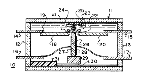
A low voltage vacuum circuit interrupter lU
hereafter "vacuum interrupter~ is depicted in Fiyure 1
and consists of a hermetically sealed envelope 11 of a
metal, glass or ceramic construction which is clo~ed
at the ends by means of endwalls 12 and 13. T~le
housing
1~80140
- 4 - 41PS 6372
either cylindrical or rectangular in configuration and
is evacuated to remove most of the air as is common
with vacuum interrupters of the higher voltage type.
For purposes of this disclosure, a low voltage
vacuum interrupter is one used for interrupting circuit
current with circuit voltages less than 1000 volts. An
example of a medium voltage vacuum interrupter is
described in U.S. Patent No. 3,014,110 in the name of
James D. Cobine, which issued December l9, 1961 which
teaches of a state of the art medium voltage vacuum
interrupting device. The low voltage vacuum
interrupter lo differs from the medium voltage vacuum
interrupter by the provision of a pair of lead-in
conductors 14, 15 for electrical connection with a pair
of fixed contacts 21, 22 attached to the ends of a
corresponding pair of shaped metal bars 18, 20 by means
of a weld as indicated at 19. A bridging contact 23 is
arranged across the fixed contact pair and is held in
good electrical connection therewith by means of a
contact spring 24 arranged on a support 25. To
separate the bridging contact from the fixed contact
pair, a piezoelectric bar 26 having a pair of electrodes
27, 28 on either side for attachment to lead-in wires
16, 17, is arranged for extension in its longitudinal
direction transverse to the electrodes for striking the
bridging contact and driving it out of electrical
connection with the fixed contact pair. The
piezoelectric bar is positioned between the bridging
contact and a metal base 29 which in turn is supported
on a cantilever spring 30. The cantilever spring is
arranged on a support 31 which is fixedly attached to
the envelope 11. The operation of the piezoelectric bar
26 is described within the aforementioned U.S. Patent
No. 4,620,122. Then the fixed contact pair 21, 22 are
electrically connected in parallel with a solid state
1~0140
- 5 - 41PS 6372
switch, the circuit current transferring between lead-in
wires 14, 15 across the contacts is first diverted
l_hrough the solid state switch before a DC voltage pulse
is applied across lead-in wires 16, 17 to drive the
bridging contact away from electrical connection with
the contact pair. Since most of the circuit current
diverts through the solid state switch, only a small
amount of current passes through the contacts at the
instant of separation. This small amount of current is
insufficient to establish an arc, particularly within
the high vacuum environment maintained within the
evacuated envelope 11. The high vacuum environment
substantially reduces the possibility of reignition
across the separated contacts when the solid state
switch turns off and circuit voltage reoccurs across the
fixed contact pair. An auxiliary switch (not shown) is
usually connected in series with the fixed contact pair
to completely interrupt the circuit path through the
contacts after the solid state switch is turned off.
A low voltage vacuum interrupter 32 is shown
in Figure 2 contained within an evacuated envelope 33
which is similar to the envelope 11 depicted earlier in
Figure 1. The envelope 33 can be metal, ceramic or
glass, depending mainly upon economic considerations.
However, the endwalls 34, 35 should be ceramic or glass
to ensure sufficient electric insulation between the
lead wires 36, 37 which support the fixed contacts 38,
39 and between the lead-in wires 41, 42 which support
the closely spaced wires 43, 44. The bridging contact
40 is carried by the closely spaced wires for
electrodynamic repulsion when a large current pulse
is passed to the lead-in wires 41, 42. A plurality
of magnetic plates 45 are arranged on either side of
the closely spaced wires to enhance the electro-
dynamic repulsion. The bridging contact 40 is
1;~8~ 0
- 6 - 41PS 6372
held in good electrical connection with the fixed
contacts 38, 39 by means of the contact spring 46
which is attached to the envelope by means of an
apertured support 47. The operation of the
electrodynamic repulsion between the closely spaced
wires 43, 44 is described within the aforementioned
Canadian Patent No. 1,245,254.
A further low voltage vacuum interrupter 48
is shown in Figure 3 to consist of an H-shaped contact
configuration 49 consisting of a stepped shaped metal
bar 50 with a formed contact 54 arranged at one end of
the step 52 integrally formed with the stepped shaped
metal bar. A second stepped shaped metal bar 51 is
arranged opposite the stepped shaped metal bar 50 such
that the fixed contact 55 formed at one end of the
step 53 is oppositely adjacent the contact 54. A
bridging contact 56 is suspended from one end of a
pair of closely spaced wires 57, 58 for electrodynamic
repulsion when a current pulse is applied to the
lead-in wires 59, 60. In a manner similar to the low
voltage vacuum interrupter depicted in Figure 2, a
plurality of magnetic plates 64 are arranged on either
side of the closely spaced wires to enhance the
electrodynamic repulsion. A pair of ceramic endwalls
67, 68 are arranged at opposite ends of the H-shaped
contact arrangement 49 to allow for electrical
insulation between the lead wires 59, 60. Electrical
connection is made with the contacts 54, 55 by means
of a separate pair of wires 61, 63 attached to the
stepped shaped metal bars 50, 51 by means of screws
62. The bridging contact is held in good electrical
connection with contacts 54, 55 by means of a contact
spring 65 attached to a U-shaped ceramic support 66.
The low voltage vacuum interrupter 48 is herme-
tically sealed by the provision of a rectangular
~80~40
- 7 - 41PS 6372
envelope (not shown) arranged on both sides of the
H-shaped contact arrangement 49. The operation of
the closely spaced wires 57, 58 to drive the bridging
contact 67 out of electrical connection with the
contacts 54, 55 is similar to that of the low voltage
vacuum interrupter 32 depicted in Figure 2. It is
noted that the electrodes 54, 55 are formed from the
B same copper material used to fabricate the stepped
shaped metal bars 50~, 51. The evacuated environment
within the low voltage vacuum interrupter allows the
use of copper electrodes without fear of oxidation.
A small amount of a reducing atmosphere, such as
hydrogen gas, can be introduced to the envelope prior
to evacuation to further ensure the absence of
oxidation over long periods of continued use. The
bridging contact 56 can have the components and
configuration of the change of state contact material
described within the aforementioned U.S. Patent No.
4,607,148. This ensures good electrical conduction
between the bridging contact 56 and the contacts 54,
55 with only a relatively small contact spring 65.
A low voltage vacuum interrupter 69 is
depicted in Figures 4, 5 and 6 which does not utilize
any contact spring whatsoever. The contacts 72, 73
are formed at one end of a pair of parallel spaced
shaped metal bars 70, 71 and electrical connection is
made therewith by means of terminal connectors 83,
84. A ceramic spacer 79 best seen in Figure 6, is
arranged such that one sidewall 81 is coextensive
with shaped metal bar 71 and an opposite sidewall
80 is coextensive with shaped metal bar 70. A
bottom extension 82 rests between the contact 72,
73 to ensure the proper spacing and electrical
insulation. A metal diaphragm 75 having an apertured
1~0140
~ 6~72
-- 8
boss 76 on an external surface thereof is herlnet1cally
sealed to the top of the ceramic spacer an~ the
bridying contact 74 is dttached to tlle interlor
side thereof. ~rhe diaphragm contains an expansion
diameter 89 to promote the flexible movement of the
diaphragm without interferillg with the hermetlc seal.
The ceramic spacer 79 is also hermetically sealed to
the shaped metal ~ars 7U, 71 to define an evacuated
space 87 on one side of the bridging contact and an
evacuated space 88 on the opposlte slde. A pair of
closely spaced wires 77, 78 are looped througn the
apertured ~oss 76 to provide a liftiny force to the
bridging contact in a manner similar to tnat described
earlier for the low voltage vacuuM interrupters
depicted in Fiyures 2 and 3. Appllcation of a hly
current pulse to the closely spaced wires 77, 78
allows the force exerted tnere~etween to pull or llft
the apertured ~oss 76, diaphragm 7S and t~le br1dyilly
contact 74 without interfering wlth the security of
the vacuUM provided within the spaces 87, ~. The low
voltage vacuwn interrupter 69 is assembled in the
manner best seen in Figure 6 wherein the spaced metal
bars 70, 71 which are formed from high purity copper,
and with the luy connectors 83, 84 fixedly attached
are arranged with the contacts 72, 73 oppositely
adjacent each other and spaced apart to allow for the
clearance of the bottoln extension 82 of the ceramic
spacer 79. The spacer is arranyed on the shaped metal
bars such that the sidewalls 80, 81 seat directly on
the shaped metal bars and the endwalls 85, 86 extend
across and seat on both of the shaped metal ~ars.
~nce the ceramic spacer 79 is in place on the shaped
metal bars, the metal diaphraglil 7S with the ~rldying
contact fixedly attached to a bottom surface an~ Wit~
the apertured boss 76 and raised dlameter 89 is tne
placed on the ceramic spacer, coextensive with the
,,
0140
- 9 - 41PS 6372
sidewalls 80, 81 and the endwalls 85, 86. Prior to
heating the assembled components to hermetically seal
the diaphragm and shaped metal bars to the ceramic
spacer, the assembly is placed in an evacuation
chamber and a vacuum is applied until the interior
spaces defined as 87, 88 in Figure 4 reach a
predetermined vacuum. The use of the evacuation
chamber during the heating and fusing of the ceramic
spacer ensures that the shaped metal bars 70, 71 remain
free of any oxidation during the fusion process. The
completely assembled low voltage vacuum interrupter 69
is depicted in Figure 5 as viewed in the plane 5-5 on
Fig. 4 which intersects the bridging contact 74 to show
the outer nickel layer 90 intermediate indium
layer 91 and silver base 92. When the low voltage
vacuum interrupter is employed with a solid state
switch to interrupt the circuit current, the bridging
contact returns to bridge across the fixed contacts as
soon as the current pulse is removed from the closed
spaced wires 77, 78. This automatic return is caused
by the atmospheric pressure acting on the flexible
diaphragm 75. The difference in pressure on both sides
of the diaphragm is equivalent to a force of
approximately 16 lbs. per square inch of diaphragm
area acting to force the attached bridging contact into
good electrical connection with the fixed contacts
without the requirement of any contact spring
whatsoever. It is within the scope of this invention
to use a gaseous material having enhanced dielectric
properties, such as SF6, and to adjust the pressure of
the gas with respect to the external atmosphere to
obtain a wide range of force on the bridging contact to
optimize the contact holding force and to obtain the
optimum contact surface configuration of the
change of state bridging contact to reduce heating
lX~30140
~ 6372
effects to a minimum.
A heavy duty double break vacuum
interrupter 93 is shown in Fig. 7 ana conslsts of a
copper bar 94 haviny an aperture 95 for connectioll
with an external electric terminal and a contact 96
fixedly attached, is arranged over a second copper
bar 98 having an aperture 99 formed at one end for
connection with the external electric circuit. The
second copper bar has a copper post lUU extending
lU perpendicular to the linear extent of the second
copper bar and supports a contact 101 Oll a top surface
thereof. A bridging contact 109 is formed on a
contact rivet lU8 which includes an apertured stem 110
passing through an apertured diaphragm 106. The
contact rivet 108 is attached to the diaphragm 106 by
means of a continuous bead 114 of silver solder. A
pair of closely spaced wires 111, 112 are arranged
through the apertured stem llU to proviae the
necessary force to lift the bridging contact lU~ from
the fixed contacts g6, 101 as previously described. A
lower ceramic disc 102 is arranged on the second
copper bar 98 to electrically insulate between the
second copper bar and the first copper bar 94. ~n
upper ceramic disc 104 is arranged between the first
copper bar and the diaphragm 106 for electrical
insulation therebetween. rrhe diaphragm contains an
expansion diameter 107 formed therein to provide for
the movement of the bridging contact and the diaphragm
without interfering with the integrity of the vacuum
formed therein when the components are evacuated and
sealed.
The double break vacuum interrupter 93 of
Fig. 7 is assembled in the manner ~est seen by
referring now to Fig. ~. The second copper bar 9~ is
arranged with respect to the first copper bar 94 such
that their respective apertures 99, 9~ are opposite
1~0140
~ 72
-- 11 --
and their contacts 101, 96 extend in the same plalle.
rrhe lower ceramic disc lU2 is placed on the second
copper bar such that the post 100 and contact 101
extelld through the aperture 103. rrhe aperture 97
i-ormed within the first copper bar 94 is positioned
such that the post 100 and contact 101 extend
therethrouyh to allow the contacts lUl, 96 to ~ecome
co-planar. The upper ceramic disc 104 is placed over
the first copper bar 94 such that both contacts extend
through the aperture 105 formed within the upper
ceramic disc. The diaphragm 106 with the ~ridging
contact lU9 on rivet 108 is positioned over the upper
ceramic disc 104 such that the bridying contact
extends through the aperture 105 to position the
bridging contact across the fixed contact lUl, 96.
The expansion diameter 107 is also arranged within
the disc aperture 105 to provide for flex of tile
diaphragm lU6 witllout interfering with the vacuum
formed when the components are later hermetically
sealed. The closely spaced wires 111, 112 arranged
through the apertured stem are accessible from the
exterior of the assembled vacuuM interrupter 93 and
the silver solder bead 114 extends around the
apertured stem as previously described. When
completely assembled, the lower disc aperture lU3
defines a first space 103A, the first copper bar
aperture 97 defines a second space 97A an~ the upper
ceramic disc aperture forms a third space 105A ~est
seen by referrring back to Fig. 7. The asselll~led
3~ components are then placed within an evacuation
chamber and are heated and sealed such that the vacuum
within the aforementioned spaces provides a re~uisite
pressure differential to force the bridging
contact 109 into excellent electrical contact with the
fixed contacts 101, 96, without the re~uirement of a
contact spring.
1;~80140
41P~ ~37
- 12 -
A low power single ~reak vacuum
interrupter 115 is show}l in Flg. 9 an~ COllSiStS of a
first copper bar 116 having an aperture 117 for
electrical connection with an external circuit an~ a
S second laryer aperture 118 which defines a space 118A,
as indicated. Within this space is arranyed an
apertured and flexible diaphragm 119 containin~ an
expansion diameter 120 and throuyh which a contact
rivet 121 is inserted and fixedly attached ~y means of
a bead 130 of silver solder. An apertured stem 126
supports a pair of closely spaced wires 122, 123 for
moving the diaphragm and the single contact 127 in the
manner described earlier. A single ceramic disc 124
is arranged between the first copper bar 116 and a
second copper ~ar 128. The second copper bar contaills
an aperture 129 at one end for electrical connectlon
with an external circuit. The sinyle corltact 127
mates with a sur~ace of the second copper bar silown
generally at 131 to provide an electrically conductive
2U path from the second copper bar 128 througn the single
contact 127 and diaphragm 119 to the first copper
bar 116. When a current pulse is dpplied to tne
closely spaced wires 122, 123 the force applied to the
contact rivet 121 lifts the diaphragm and the single
contact out of contact with the second copper bar 128
to interrupt the electrical connection between the
first and second copper bars.
The low power single break vacuum
interrupter of Fig. 9 is assembled in the Jnanner
depicted in Fig. 10 and descri~ed as follows. The
second copper bar 128 is arranged with the
aperture 129 oriented opposite from the aperture 117
through the first copper bar 116. The ceramic
disc 125 is then arranged on the second copper bar
such that the aperture 125 surrounds tlle contact
Mating surface generally shown at 125A in Fiy. 9. rrhe
~;~S0~40
41PS b37 2
-- 13 --
i-lexible diaphragm 119 is placed Oll the cerdlnic disc
with the expansion diameter 12~ within tile disc
aperture and with tne COIltdct rivet 121 and apertured
steln 126 concentrically arranged within tne
aperture 11~ provided throuyn t~le first copper bar and
with the closely spaced wires 122, 123 extelldilly
throuyh the aperture. When the compollellts are
assembled as depicted in Fig. 9, they are placed
within a evacuation chamber and are evacuated and
sealed in the manner described earlier. The low power
single contàcts vacuum interrupter 115 is useful in
circuits wherein the current transport throuyh the
flexible diaphragm 119 is insufficient to cause excess
heating of the diaphragm.
It is thus seen that the use of a solid
state switch across a pair of contacts contained
within an evacuated chaJnber allows the contacts to
rapidly separate to interrupt circuit current with
little or no deterioration due to arciny or cheullcal
activity. The vacuum also allows the circuit to
interrupt upon the occurrence of a very small
separation distance because of the excellent
dielectric porperties inherent in the vacuum
environment.