Note: Descriptions are shown in the official language in which they were submitted.
~o~9
PHN 11.593 l 7.4.1986
Phase-locked loop coefficient generator for a filter
arrangement having a non-rational ratio between input and
output sampling frequencies.
A. BACKGROUND OF TH~ INVENTION.
A(1) Field of the invention.
The invention relates in broad outline to an
arrangement for changing the sampling frequency fi of a
discrete-time signal into a sampling frequency fu. An
arrangement of this type will hereinafter be referred to as
sample rate converter and the ratio fu/fi will be referred
to as the conversion factor. The invention particularly
relates to a sample rate converter in which the conversion
factor is non-rational (for example, ~2 or 1/ ~ ).
A~2) Descrlptlon of the pxio_ art .
Sample rate converters have been generally known
for many years. They are used to lncrease or decrease the
sampling frequency of a discrete-time signal. In the former
case, the converter is sometimes referred to as an inter-
polator, in the latter case as a decimator. For a general
background about interpolators and decimators, reference is
made to the references 1-6 in section C.
A sample rate converter generally comprises a
signal processing circuit. The discrete-time signal is
applied thereto as an input signal whose sampling fre-
quency must be changed and furthermore it receives so-called
filter coefficients. It supplies the desired discrete-time
signal as an output signal. Each sample of this ~iscrete-
time output signal is equal to the sum of a number of,
for example, M samples of the discrete-time input signal in
which each of these input samples is weighted with a filter
coefficient.
To calcul~e an output sample, a group of M fllter
coefficients must be principally available. These filter
coefficients are supplied by a filter coefficient generator
~0159
PHN 11.593 2 7.4.1986
and, as is known, they represent samples of the finite
pulse response h(v) of a predetermined filter (v is a con-
tinuously variable in the interval - GO < v <oo).
If the sample rate converter is a decimator and if
s the conversionfactor is 1/R, with R being an integer, it does
not supply an output sample until after it has received
R input samples. For the calculation of each output sample
the same group of M filter coefficients is used. A memory
in which the M filter coefficients are stored may be used
as a filter coefficient generator.
If the sample rate converter is an interpolator and
if the conversion factor is equal to R, it supplies R out-
put samples whenever a new input sample has been received.
For each of these R output samples the filter coefficient ge-
nerator must supply an appropriate group of filter coeffi-
cients. Also in this case a memory in which the required
(for example, RM) filter coefficients are stored may be used
as a filter coefficient generator.
When, as in the above described cases, the quanti-
ty R is an integer, the required filter coefficients are in-
variable. The situation is entirely different when R is
non-rational. In that case the required filter coefficients
for each output sample must be calculated separately.Filter
coefficient generators that can fulfil this task have been
described extensively in references 7 and 8 More particular-
ly, reference 7 describes a decimator, whereas reference 8
describes an interpolator. Each filter coefficient generator
used therein comprises a deviation circuit to which on the
one hand clock pulses occurring at a "low" rate fl (herein-
after referred to as low-rate clock pulses) and on the other
hand clock pulses occurring at a "high" rate fh (herein-
after referred to as high-rate clock pulses~are applied. Each
time after a low-rate clock pulse has occurred, this deviat-
ion circuit supplies a deviation d whose magnitude is pro-
portional to the ratio between the time interval Td betweenthis low-rate clock pulse and the immediately subsequent or
immediately preceding high-rate c].ock pulse and the time
~30159
P~IN 11.593 3 7.4.1986
interval l/fh between two consecutive high-rate clock pulses.
In a mathematical form this is:
d = Td fh (1)
The deviation d thus obtained is applied to a cal-
5 culation circuit which, starting from the predetermined pulseresponse h(v), calculates the required filter coefficients.
When the mth filter coefficient to be calculated is symboli-
cally represented by a(m), there applies that:
a(m) = h (d+m)/fh (2)
If the sample rate converter is a decimator, as in
reference 7~ fh is equal to the sampling frequency fi of the
input signal and fl is equal to the sampling frequency fu f
the output signal. If the sample rate converter is an inter-
polator, these equalities are reversed.
B . OBJECT AND SUMMARY OF THE INVENTION .
The deviation circuits as extensively described
in the said references 7 and 8 are found to require a con-
siderable amount of hardware in practice.
It is therefore an object of the invention to pro-
vide a simpler embodiment of a deviation circuit of this type.
According to the invention the deviation circuit
comprises
- a phasedetector to which the low-rate clock pulses are
applied on the one hand and to which synthetic low-rate clock
pulses are applied on the other hand and which supplies a
discrete-time phase difference signal;
- a counter circuit adapted to receive a reference value,
which circuit receives the high-rate clock pulses as count-
ing pulses and supplies a synthetic low-rate clock pulse
for the phase detector each time after receiving a number of
high-rate clock pulses which is equal to the reference value;
and
- a processor circuit which receives the discrete-time phase
difference signal and in response thereto supplies deviat-
ions d at the low rate fl as well as reference values for
the counter circuit.
Functionally, this deviation circuit constitutes a
~ _,
~01~9
PHN 11.593 4 7.4.1986
phase-locked loop in which a generator is used as a voltage-
controlled oscillator supplying a sawtooth signal, the height
of the sawtooth being determined by the phase difference
signal and the slope being constant.
The implemented phase-locked loop as defined above
does not, however, actually supply this sawtooth signal in a
complete form. On the other hand the processor circuit
supplies a reference value which indicates how many high-
rate clock pulses fit into one period of the sawtooth signal
and this period must be equal to the period with which the
low-rate clock pulses are applied to the phase detector. The
processor circuit which is used in combination with the
counter circuit for generating the synthetic clock pulses is
a]so used for calculating the deviation d so that no extra
hardware is required for this purpose.
C. REFERENCES.
-
1. A Digital Signal Processlng Approach to Interpolation;R.W.Schafer, L.R.Rabiner;
Proceedings of the IEEE, Vol. 61, No. 6, June 1973, pages
692-702.
2. Arrangement for Converting Discrete Signals into a Dis-
crete Single-Sideband Frequency Division-Multiplex-Signal
and Vice Versa;
T . A .C.M.Claasen, W.F.G. Mecklenbrauker;
United States Patent Specification No. 4,131,764.
(This Patent Specification is equivalent to Netherlands
Patent Applicatlon No. 77,03,633 (PHN 8731)).
3. Low Pass Nonrecursive Digital Filter;
M, Bellanger, G.G. Lepagnol, J. Daguet;
United States Patent Specification No. 3,928,755.
(This PatentSpecification is equivalent to Netherlands Patent
Application no. 74,00,761 (PHN 6883)).
4, Interpolating Digital Filter;
LD.J.Eggermont, H.A. van Essen, P.J. van Gerwen, W.A.M.
Snijders;
United States Patent Specification no. 3,988,607.
,",~.,
:
: .
.
~2~301S9
PH~ 11.593 5 7.4.1986
(This patent specification is equivalent to Netherlands Pa-
tent Application No. 74,12,224 (PHN 7733)).
5. Interpolating Digital Filter with Input Buffer;
H.A. van Essen, N.A.M. Verhoeckx, W.A.M.Snijders;
5 United States Patent Specification no. 3,997,773.
(This patent specification is equivalent to Netherlands
Patent Application no. 74,12,225 (PHN 7729)).
6. Interpolation-Decimation Circuit for Increasing or De-
creasing Digital Sampling Frequency;
R.E.Crochiere, L.R.Rabiner;
United States Patent Specification no. 4,020,332.
7.Decimation Filter Arrangement;
E.P. Stikvoort;
Published European patent application no. 0,099,600 (PHN
10 394).
8. Interpolating Filter Arrangement with Inrational Ratio
between the Input and the Output Sampling Frequencies;
E.P. Stikvoort;
Published European patent application no. 0,151,829 (PHN
10 899).
D. BRIEF DESCRIPTION OF THE FIGURES
Fig. 1 diagrammatically shows the general struct-
ure of a sample rate converter;
Fig. 2 shows the theoretical model of the phase-
locked loop shown in Fig. 1;
Figs. 3, 4 and 5 show some diagrams to explain
the operation of the filter coefficient generator shown in
Fig. 1;
3~ Fig. 6 shows the flow chart for programming the
processor shown in Fig. 1;
Fig. 7 shows an embodiment of a loop filter; and
- Fig. 8 shows an embodiment of a digital phase de-
tector.
E. DESCRIPTION OF THE EMBODIMENTS.
E ~1 j General structure of a sample rate converter.
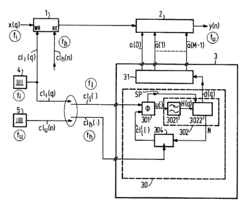
Fig. 1 diagrammatically shows the general structure
30~59
PHN 11.593 6 7.4.1986
of a sample rate converter having a non-rational conversion
factor. It is provided with an input buffer 1 through which
t:he input samples x(q) which occur at a rate fi are applied
to a signal processing device 2 supplying output samples
y(n) at the desired rate fu. For calculating each output
samples y(n) the signal processing device 2 also receives M
filter coefficients a(O), a(1), ... a(M-1) from a filter
coefficient generator 3.
The buffer 1 has a write input W and a read input
lo RE. The write input WR receives a clock signal cl1 con-
sisting of clock pulses cli(.) occurring at the input
sampling frequency fi. The input sample x(q) is stored in
this buffer in response to a clock pulse cli(.). The read
input RE receives a clock signal clh consisting of
clock pulses clh(.) which occur at a frequency fh and will
be referred to as high-rate clock pulses. Whenever such a
high-rate clock pulse clh(.) occurs, the contents of the
buffer are transferred to the signal processing device 2
and the bufer is also reset. Thus it is achieved that if
no input sample is stored in the buffer between two conse-
cutive high-rate clock pulses, a sample having the value
zero is applied to the signal processing device 2. This
situation occurs when the sample rate converter is an inter-
polator.
The signal processing device 2 may be implemented
in known manner. For example, in the manner as described in
reference 7 when the sample rate converter is a decimator
and in the manner as described in reference 8 when it is an
interpolator.
The clock pulses cli(.) occurring at the input
sampling frequency fi are supplied by a clock pulse generator
4. It will be assumed that there is also a clock pulse gene-
rator 5 supplying a clock signal consisting of the clock
pulses clu(.) occurring at the output sampling frequency f
Since a sample rate converter is concerned in this case,
the output sampling frequency will be either higher or lower
than the input sampling frequency. The previously mentloned
clock signal clh consisting of the high-rate clock pulses
:, ~
.
1~0~9
PHN 11.593 7 7.4.1986
clh(.) is now formed by one of the two clock signals cli
and clu, more specifically by the clock signal whose clock
pulses occur at the highest rate. For the purpose of simpli-
fication of the following, the other clock signal will be
indicated by cll, and its clock pulses with cll(.). The
rate at which these clock pulses occur will be indicated by
fl and they will be referred to as low-rate clock pulses.
The clock pulses clh(.) and cll(.) are applied
to the filter coefficient generator 3 and utilized therein
for calculating the deviation d on the one hand and the re-
quired coefficients a(m) on the other hand. To this end
this filter coefficient generator 3 is provided with a phase-
locked loop 30 and a calculation device 31. In response to
each low-rate clock pulse cll(.) the phase-locked loop 30
supplies a deviation d(.) which is applied to the calculation
device 31 (for example, a microcomputer). The latter is
adapted to calculate the re~uired filter coefficients at the
given value of d~.) in accordance with expression (2).
The phase-locked loop 30 comprises more parti-
cularly a phase detector 301, a processor circuit 302 and
a counter circuit 3~4.
In the embodiment shown the processor circuit
302 is constituted by the cascade arrangement of a loop
filter 3021 and a processor 3022. The phase detector 301 re-
ceives the low-rate clock pulses cll(.) at one of its inputs
and synthetic low-rate clock pulses cl'l(.) at the other
input, which latter pulses are supplied by the counter cir-
cuit 304. This phase detector supplies a discrite-time
phase difference signal u in which each phase difference
sample u(.) is a measure of the time interval between a
clock pulse cll(.) and the immediately subsequent or imme-
diately preceding synthetic clock pulse cl'l(.). The dis-
crete-time phase difference signal thus obtained is subject-
ed in the loop filter 3021 to a discrete-time filter pro-
cessing operation. As a result of and in response to eachlow-rate clock pulse cll(.) this loop filter supplies a
control signal sample H(.) which is processed ln the pro-
.
.
l~aol~9
PHN 11.593 8 7.4.1986
cessor 3022. This processor is programmed in a manner to bedescribed hereinafter so that on the one hand it supplies
the deviationd(.) and on the other hand a number N(.) which
indicates how many high-rate clock pulses fit into one
s period of a hypothetical sawtooth signal having the same
slope in each period but whose sawtooth height and thus also
the actual period is proportional to the actual control
signal sample H(.) supplied by the loop filter. This number
N(.) is applied to the counter circuit 304. This circuit
lo 304 also receives the high-rate clock pulses via a clock
pulse input and supplies a synthetic clock pulse cl'l(.)
when N(.) high-rate clock pulses have been received. There-
fore this counter circuit 304 may advantageously be desig-
ned as a presettable down counter.
It is to be noted that the phase detector 301
supplies a control pulse SP simultaneously with a phase
difference sample u(.), whlch pulse Is applied to the pro-
cessor circuit for its lnltlallsatlon.
E(2) Theoretlcal backqround of the inventlon.
The embodiment of the phase-locked loop shown in
Fig. 1 is a pratical embodiment of the theoretical model
shown in Fig. 2. In addition to the phase detector 301 and
the loop filter 302, this model comprises a sawtooth oscilla-
tor 305 and a differentiating network 306. The phase detec-
tor 301 again receives the low-rate clock pulses cll(.) and
cl'l(.) and supplies in response to each low-rate clock
pulse a difference signal sample u(.) which is a measure of
the phase difference between the last received low-rate clock
pulse cll(.) and the immediately subsequent or immediately
preceding low-rate clock pulse cl'l(.). After filterlng
of the phase difference samples by the loop filter 3021,
a control signal sample H(.) is obtained which controls the
sawtooth oscillator 305. All sawteeth supplied by this
oscillator have the same slope. Their tooth height is, how-
ever, equal or proportional to the actual control signalsample H(.). Whenever the sawtooth has reached this tooth
height, a new sawtooth starts and the differentiating net-
., .
0~9
PHN 11 .593 9 7.4.1986
work 306 supplies a low-rate synthetic clock pulse cl'l(.).
When the loop is not locke~, there is a phase
difference between two low-rate clock pulses. This situation
is shown for completeness' sake in Fig. 3. More pa~ticularly
Fig. 3 shows at A a number of low-rate clock pulses cll(.),
at B a number of synthetic low-rate clock pulses cl'l(.) and
at C the output signal z(t) of oscillator 305.
When the loop is locked, there is a minimum phase
difference between the two low-rate clock pulse signals
cll and cl'l. This situation is shown for completeness' sake
in Fig. 4. More particularly this Fig.4 shows at A again a
number of low-rate clock pulses cll(.), at B a number of
low-rate clock pulses cl'l(.) and at C the output signal
z(t) of oscillator 305.
As is shown in Fig. 2, the output signal z(t) of
the sawtooth oscillator 305 is first sampled in the sampler
307 for calculating the consecutive deviations d(.), the
high-rate clock pulses clh~.) being used as sampllng pulses.
A number of these high-rate clock pulses is shown at D in
Fig. 4. In response to these clock pulses the sampler
supplies the sawtooth samples z(.) shown at E in Fig. 4 of
the sawtooth signal z(t) shown at C in Fig. 4. In the dia-
gram shown at E the original sawtooth signal is shown in
broken lines for completeness' sake. These sawtooth samples
Z(-) are furthermore applied to a calculator circuit 308
calculating a new deviation d(.) whenever a control pulse
SP has occurred and applying this deviation to its output.
To indicate how this deviation d(.), which is mathematically
formulated in expression (2), is calculated by using the saw-
tooth samples z(.), the part of the diagram shown at E inFig. 4 between the points P and Q is enlarged in Fig. 5.
In this Figure a number of points have been indicated by
a, b, c, e, g, k, m. In accordance with expression (2) there
applies that:
d(q) = Td~q) fh-
In this expression Td(q) represents the distancebetween the low-rate clock pulse cll~q) and the immediate-
'~` - . ,
~ o~9
PHN 11.593 10 7.4.1986
ly subsequent high-rate clock pulse clh(n+1), or the imme-
diately preceding high-rate clock pulse clh(n). The start-
ing point hereinafter will be that Td(q+1) is the distance
between cll(q) and clh(n+1) so that this distance corres-
ponds to the line section gc. The reciprocal value Th f fhrepresents the distance between two consecutive sawtooth
samples and thus corresponds to the length of the line section
ab. Furthermore the line sections gk and em correspond to
H(q-1) and the length of the line section ec corresponds to
z(n+1). Since each sawtooth has the same slope, the dif-
ference between two consecutive sawtooth samples within
one and the same period is constant. This constant has the
- magnitude incr. Since the line section eb represents such a
difference, the length of this line section corresponds to
incr. In accordance with the known rules of planimetry it
then follows that
d(q) = z(n+1)/incr. (3)
It follows that for calculating the deviation d(.) it is
sufficient to know the value of the first sawtooth sample
taken from a sawtooth.
The present invention is bas~ on the recognition
that this sawtooth sample can be calculated and that the
consequence thereof is that the sawtooth oscillator 305
shown in Fig. 2 is no longer physically present in the
sample rate converter according to the invention. More par-
ticularly z(n+1) can be derived from z(n-4). In fact, as is
apparent from Fig. 5:
z(n+1) = z(n-4) + 5 incr. - H(q-1) (4)
In this expression the number 5 indicates that z(n+1) is the
fifth sawtooth sample after z(n-4). To genera1iseexpression
(4)m it is to be noted that a new sawtooth does not start
until after a difference signal sample u(.) has occurred,
whilst the qth sawtooth commences after the qth difference
signal sample u(q) has occurred. When the first sawtooth
sample taken from the qth sawtooth is represented by s(q)
and when furthermore the number of high-rate clock pulses
occurring within the period of this qth sawtooth (or, iden-
01~9
PHN 11.593 11 7.4.1986
tically, the number of sawtooth samples from this qth saw-
tooth) is equal to N, there generally applies that
s(q) = s(q-1) + N incr - H(q-1) (5)
so that
d(q) = s(q)/incr = N + ~s(q-1)-H(q-1)~/incr (6)
In this expression the quantities s(q) and N are unknown.
The quantity incr is fixed and known by choice. The
quantity H(q-1) is supplied by the loop filter, the quantity
s(q-1) is known because this is the result either of a pre-
ceding calculation or because it is a known initial value.
In spite of all these known quantities expression (6)com-
prises s(q) as the desired quantity but also N as an un-
known quantity. In order to be able to calculate the de-
sired sawtooth sample s(q) it should be considered that
0 ~ s(q)~incr (7)
and hence
0 ~ s(q)/incr < 2 (8)
while N ~ 2 (9)
In other words, if a number P can be found which is equal to,
for example, the difference
p = -N + s(q)/incr
and which consists of the sum of two numbers P1 and P2 in
which, for example, P1 ~ 1 and P2 ~ 1, then it holds that
d(q) = s(q)/incr = P1
N = P2 (10)
Such a number P exists indeed and can be calculated.
In accordance with expression (6)
-N + s(q)/incr = ~s(q-1) - H(q-1)~/incr = P (11)
E(3) The processor 3022.
The quantity P indicated in expression ~11) ls
calculated by the processor 3022 which may be a microcom-
puter. It may be, for example, a microcomputer of the MAB
8000 family in which the steps shown in Fig. 6 are carried
out. A calculation cycle starts some time after the phase
detector 301 has supplied a control pulse SP. After the last
supplied phase difference sample has given a contribution to
the new control sample H(q-1) which is supplled by the loop
. ~
.
~01~9
PHN 11.593 12 7.4.1986
filter, this sample H(q-1) is read by the processor and
stored in a work register intended for this purpose (step
302(0)). Subsequently the last calculated sawtooth sample
s(q-1) stored in a storage location intended for this pur-
5 pose and referred to as S store is transferred to a furtherwork register (step 302(1)). These two data are subsequent-
ly subtracted from each other in a step 302(2) and divided
by the number incr. As a result the desired number P is ob-
tained which is stored in a P-register (step 302(3)). In a
lo step 302(4) the bits of P having a significance which is
larger than or equal to 2 and thus represent the number N
are subsequently applied to the counter circuit. In a fur-
ther step 302(5) the bits of P having a significance of
less than 2 and thus representing the deviation d(q) are
applied to the calculation device 31. Subsequently the de-
viation d(q) is multiplied by the number incr in a step
302(6) so that the number s(q) is obtained. Finally the saw-
tooth sample s(q-1) is replaced by s(q) in the S store in a
step 302(7).
E(4) The loop filter.
Fig. 7 shows an embodiment of a loop filter 3021.
It is of the discrete-time type and comprises counter cir-
cuits 30211 and 30212, three delay circuits 30213, 30214 and
30215 each having a delay period Tl and three multipliers
30216, 30217 and 30218 with the respective multiplication
coefficients C0, C1 and C2 supplied by a coefficient gene-
rator 30219. These elements are interconnected in the manner
shown in the Figure such that a transfer function is realised
which is equal to:
30 C2(1+CoZ 1)/(1-Z 1) (1-C1Z 1) (12)
In a practical embodiment the multiplication coefficients
were chosen as follows:
C0 = b-1
C1 = 1-32b (13)
C2 = -1/2 w2
b = 2 W.
W is a number to be chosen in the range of 10 2 to 10 7 in-
.~ ,
~o~s9
PHN 11.593 13 7.4.1986
clusive. This number W need not be a fixed number. In the
embodiment shown the coefficient generator 30219 receives the
phase difference signal and based thereon it calculates a
value for W so as to calculate subsequently the coefficients
5 with this value for W in accordance with expression (13). The
loop filter thus obtained is referred to as an adaptive
filter.
As is known, the embodiment of the loop filter shown
in Fig. 7 may also be considered as a flow diagram for a
o software implementation. This means that such a loop filter
can also be implemented in known manner in software in the
processor 3022.
E(5) The ~ase detector.
Fig. 8 shows an embodiment of a digital phase de-
tector 301. It is provided with a device 3011 to which the
low-rate clock pulses cll(.) are applied. After having re-
ceived a clock pulse cll(.) this device supplles a pulse in
phase with a high-rate clock pulse clh(.). The output sig-
nal of this device 3011 as well as the synthetic low-rate
clock pulses cl'l(.) are applied to a control circuit 3012
supplying an up command UP or a down command DWN for an
up-down counter 3013. The latter counter also receives the
high-rate clock pulses clh(.) as counting pulses. The con-
tents of this counter are transferred to the processor cir-
cuit at the instant when the control pulse SP occurs.
In the embodiment shown the control circuit 3012consists of 2 JK flip-flops 30121 and 30122 and an AND gate
30123 which are connected together in the manner shown. The
JK flip-flops are of the type having a clock pulse input.
The high-rate clock pulses are applied thereto.
The pulse supplied by AND-gate 30123 resets the two
JK flip-flops and also sets a further flip-flop 3014 which
in response thereto supplies the previously mentioned control
pulse SP starting, inter alia, the program shown in Fig. 6.
~ ~'