Note: Descriptions are shown in the official language in which they were submitted.
1~80i64
Technlcal Fleld
Thls lnventlon relates to an electronlc measurlng devlce tor
assesslng the ablllty of a storage battery or other dc source o~
electrlclty to dellver power to a load. ~ore speclflcally, lt relates
5 to lmproved apparatus of the type dlsclosed ln U.S. Patent
~,87~,91 1, ELECTRONIC BATTERY TESTING DEVICE, lssued to Kelth S.
Champlln, March 25, 1975, and of the type dlsclosed ln U.S. Patent
3,909,708, ELECTRONIC BATTERY TESTING DEVICE, lssued to Kelth S.
Champl ln, September ~0, 1975.
~gund Art
Storage batterles are employed ln many appllcatlons requlrlng
electrlcal energy to be retalned for later use. Most commonly, they
15 are employed ln motor vehlcles utlllzlng lnternal combustlon
englnes. In such appllcatlons, energy stored ~y "charglng" the
~attery durlng englne operatlon ls later used to power llghts, radlo,
and other electrlcal apparatus when the englne ls stopped. The most
severe demand upon the battery of a motor vehlcle ls generally made
20 by the self-starter motor. Typlcally, several k~lowatts of power are
requlred by the self-starter motor to crank the englne. Fallure to
satlsfactorlly accompllsh thls task, partlcularly ln cold weather, ls
usually the flrst lndlcatlon o~ battery deterloratlon or trou~le wlth
the charglng system. Clearly, a simple measurement that
.
~<~30~4
accurately assesses a battery's a~lllty to supply power is of
conslderabte value
Prlor to the pu~llcatlon ot U.S. Patents 3,873,911 and
~,909,708, a ~attery's ablllty to supply power was customarlly
assessed by means o~ a load test. A load test sub~ects a battery to a
5 heavy dc load current havlng a predetermlned value dlctated by the
battery's ratlng and temperature. After a prescrlbed tlme lnterval,
the battery's termlnal voltage under load ls observed. The battery ls
then consldered to have ~passed" or "~alled" the load test accordlng
to whether thls termlnal voltage ls greater than, or less than, a
lO partlcular prescrlbed value. Although the load test has been wldely
used tor many years to tleld-test storage batterles, lt possesses
several serlous dlsadvantages. These lnclude:
1 Currents drawn are very large and theretore requlre
apparatus that ls heavy and cumbersorne.
2. Because ot these large currents~ conslderable ~sparklng" can
occur at the battery termlnals lr the test apparatus ls connected or
dlsconnected under load condltlons. Such nsparklng~ ln the presence
o~ battery gasses can cause an exploslon wlth potentlally serlous
in~ury to the operator.
3. A load test leaves the battery in a signlficantly reduced
state of charge and therefore less capable o~ cranklng the englne
than before the test was per~ormed.
4. Slnce the battery's termlnal voltage drops contlnuously
wlth tlme durlng the load test, the test results are lmpreclse and
25 greatly dependent upon the sklll or the operator.
~0164
5 Load test results are not repeatable slnce the test ltself
temporarlly polarlzes the ~attery. Such test-lnduced polarlzatlon
slgnltlcantly alters the lnltlal condltlons of any load tests
pertormed subsequently.
A practlcal alternatlve to the common load test ls taught ln
U.S. Patent ~,873,91 l and U.S. Patent 3,909,708. Both o~ these
patents dlsclose electronlc apparatus tor accurately assesslng a
battery's condltlon by means ot small-slgnal ac measurements o~ lts
dynamlc conductance. These two patents teach that a battery's
10 dynamlc conductance ls directly proportlonal to lts dynamlc power;
the maxlmum power that the battery can dellver to a load. ~ynamlc
conductance ls theretore a dlrect measure ot a battery's electrlcal
condltlon. Vlrtually mllllons ot battery measurements pertormed
over the course ot thlrteen years have tully corroborated these
15 teachlngs and have proven the valldlty or thls alternatlve testlng
method.
In comparlson wlth the load test method ot battery appralsal,
the dynamlc conductance testlng method taught ln U.S. Patents
3,873,9 l l and 3,909,708 has many advantages. For example,
20 dynamlc conductance testlng utlllzes electronlc apparatus that ls
small and llghtwelght, draws very llttle current, produces vlrtually
no ~'sparklng" when connected or dlsconnected, does not appreclably
dlscharge or polarlze the battery, and ylelds very accurate,
reproduclble, test results.
Two electronlc battery tester embodlments are dlsclosed ln
U.S. Patent 3,873,9l l; each ot whlch accurately determlnes a
~0164
battery~s dynamlc conductance and provldes the operator wlth a
numerlcal readlng that ls dlrectly proportlonal to thls quantlty. The
flrst embodlment comprlses a brldge clrcult that ls brought to
~alance by the operator to obtaln the numerlcal readlng. The
s preterred second embodlment provldes the operator wlth a dlrect
readout that may be dlsplayed numerlcally on a dlgltal or analog
meter. ~he operatlng prlnclples o~ tne pre~erred, dlrect-readlng,
second embodlment ot the lnventlon taught ln U.S. Patent 3,873,9l l
are based upon the theory of hlgh-galn feedback ampll~lers.
o U.S. Patent 3,909,708 llkewlse dlscloses two electronlc
battery tester embodlments. However, ~rom the operator's polnt ot
vlew, thelr operatlon more closely resembles the operatlon ot a
tradltlonal load-test apparatus than does operatlon ot elther ot the
numerlcal-readlng em~odlments dlsclosed ln U S Patent ~,87~,9l 1 .
15 Rather than obtalnlng a numerlcal measurement, the operator makes
prellmlnary adJustments to knobs on the panel ot the apparatus;
settlng them to the electrlcal rat~ng and temperature o~ the battery
undergolng test. The dlsclosed apparatus then employs small-slgnal
measurements o~ dynamlc conductance to slmply ascertaln whether
20 or not the battery ls capable o~ dellverlng an amount o~ power
approprlate to the battery's ratlng and temperature. Accordlngly,
the two embodlments dlsclosed ln U.S. Patent 3,909,708 provlde
slmple "pass-tall~ battery condltlon lnformatlon, Just as does
conventlonal load test apparatus. However, they accompllsh thls
25 result wlthout drawlng a large current trom the battery and are
therefore not sub~ect to the serlous dlsadvantages of a load test.
301~i4
Just as wlth the second embodlment dlsclosed tn the earller patent,
the operatlng prlnclples of the second, preterred, embodlment
dlsclosed ln U.S. Patent 3,909,708 are based upon the theory o~ hlgh-
gatn ~eed~ack amplltlers.
Both preterred embodlments of electronlc battery testlng
5 devlces, the second embodlment dlsclosed ln U.S. Patent ~,873,9 l l
and the second embodlment dlsclosed ln U.S. Patent 3,909,708, are
~ased upon feedback ampllfler prlnclples. The orlglnal
lmplementatlons ot these electronlc ~attery testlng devlces ~oth
utlllzed contemporary solld state devlce technology. Such
technology was, however, llmlted to only dlscrete devlces such as
blpolar translstors and dlodes, and small-scale lntegrated (SSI)
clrcult verslons ot slngle-element monollthlc operatlonal
amplltlers.
Great advances have been made ln sol~d-state lntegrated
15 clrcult (IC) technology durlng recent years. In partlcular, hlgh
performance complementary metal-oxlde-semlconductor (C~10S) and
blpolar r~edlum-scale lntegrated (~1SI) clrcults, such as dual and
quad operatlonal amplltlers, have ~ecome a~undantly avalla~le at
very low prlces. Therefore, important advantages, of both technlcal
20 and economlc natures, could currently be reallzed by exploltlng thls
newer, more advanced, solld-state devlce technology ln the
electronlc ~attery testlng art
Unfortunately, a num~er of deslgn consideratlons preclude the
slmple lntroductlon of the newer IC technology lnto the teedback-
25 ampllrler type o~ electrontc ~attery tester clrcultry dlsclosed ln
1~ ~3O~6L~
U S. Patents 3,873,9 l t and ~,909,708. Foremost among theseconslderatlons are the var~ous pro~lems lmposed ~y the tact that the
commerclally avallable C~OS and ~lpolar MSI iCs do not provlde
separate pln-outs tor supplylng power to the lndlvldual elements on
the chlp. However, the orlglnal dlscrete-element feedbac~ amplltler
5 deslgns relled heavtly upon the avallablllty of such separate power
connectlons. In partlcular, the orlglnal deslgns requ~red separate
connectlons ~or supplylng power to dlt~erent actlve devlces ln order
to lmplement "tour-polnt probeU archltecture and ttlere~y ellmlnate
the spurlous reslstance ot the connectlng leads and ~attery contacts
10 ~rom the measurements; ln order to reallze a preclsely-leveled
osclllator voltage and thereby obtaln lncreased measurement
accuracy; and ln order to lmplement synchrono~ls detectlon ot the
arnpllfled osclllator slgnal and thereby suppress measurement
errors caused by spurlous plckup ot hum and nolse. Accordlngly,
15 ma~or changes ln the bas~c deslgn o~ the electronlc battery tester
embodlments would be requlred before one could reallze any ot the
potenttal techn1cal and economlc ~enetlts assoclated wlth the
newer, more ettlclent and more cost-eftectlve, IC technology.
~ummary ot the Inventlon
The lmproved electronlc ~attery testlng devlce ln accordance
wlth the present lnventlon lncorporates the ~unctlons ot both of the
25 two earller-dlsclosed feedback-type electronlc battery testlng
1~016~
devlces ln a slngle embodlment. By vlrtue of novel deslgn
lnnovatlons dlsclosed hereln below, tne need ~or separate power
connectlons to dlf~erent actlve devlces ls ellmlnated, thus
permlttlng the successful lntegratlon of CMOS and ~lpolar ~ISI ICs
lnto a practlcal battery tester lmplementatlon. Thls results ln the
reallzatlon o~ a very slmple electronlc battery testlng devlce that ls
relatlvely lnexpenslve to manufacture, but whlch provldes a very
hlgh degree ot measurement accuracy. Dlsclosed lnnovatlons, whlch
clrcumvent the need tor separate connectlons to supply power to
dltterent actlve elements, lnclude:
o l. A novel technlque ~or ln~ectlng the osclllator slgnal lnto
the reedback ampll~ler~s lnput clrcult The dlsclosed tn~ectlon
technlque permlts utlllzlng a common power source tor both the
osclllator and the teedback amplltler. Nevertheless, lt malntalns
suttlclent lsolatlon ~etween the ampll~er's lnput and output
15 clrcults to allow the spurlous reslstance ot the ~attery leads and
contacts to be ettectlvely ellmlnated trom the measurements by
means of ~tour-polnt probe~ archltecture.
2. A novel, preclsely-leveled, osclllator lmplementatlon
employlng an operatlonal ampllfler, a C~10S bllateral analog swltch
20 and a zener dlode. Thls slmple clrcult utlllzes an unregulated,
common, power supply ~ut provldes an output slgnal of preclsely
malntalned amplltude; thus permlttlng hlgh measurement accuracy.
3. A novel synchronous detector lmplementatlon employlng a
C~lOS bllateral analog swltc~ along wlth an operatlonal ampll~ler
25 employed as an lntegrator. Thls slmple clrcult also obtalns power
~Ol~i
through common connectlons whlch supply power to all other actlve
devlces. It ls theretore powered contlnuously and thus dlffers
tundamentally trom the synchronous detector clrcult dlsclosed
earller ln U.S. Patent 3,909,708 WhlCh requlres that lts power
source be lnterrupted perlodlcally at the osclllator rrequency.
Nevertheless, the new synchronous detector lmplementatlon
provldes accurate, llnear detectlon of the ampllrled osclllator slgnal
whlle effectlvely suppresslng externally generated hum and nolse
that ls uncorrelated wlth the slgnal generated by the battery
tester's lnternal osclllator.
o The lmproved electronlc battery testlng devlce hereo~ can be
used tor obtalnlng elther a qualltatlve or a quantltatlve assessment
ot a wlde varlety ot dc energy sources. In addltlon to automotlve-
type batterles, the lnventlon can be used to test many other dc
energy sources such as other types ot lead-acld batterles as well as
15 nlckel-cadmlum batterles; llthlum batterles; solar ~atterles; ruel
cells; thermo-etectrlc generators; thermlonlc generators; and
magneto hydro-dynamlc generators. The lnventlon hereot Is wldely
appllcable to testlng SUCh dc energy sources by vlrtue ot lts
slmpl~clty, lts sarety~ lts accuracy, lts ease or operatlon, and lts
20 lOw cost.
Brlet Descrletlon or the Drawlngs
Flg. I ls a slmpl~fled block dlagram ot an lmproved electronlc
25 battery testlng devlce ln accordance wlth the present lnventlon.
~301~4
Flg. 2 ls a slmpllfled schematlc dlagram of a sectlon of the
block dlagram ot Flg. l dlscloslng four-polnt pro~e~ archltecture for
lnterconnectlng the hlgh-galn amplltler, the osclllator, and the
battery undergolng test.
Flg. 3 ls a stmplltled schematlc dlagram, slmllar to that
dlsclosed ln Flg. 2, but showlng connectlons requlred ~or provldlng
osclllator power ln accordance wlth the teachlng of U.S. Patents
~,873,9 l l and 3,909,708.
Flg. 4 ls a slmpllfled schematlc dlagram, slmllar to that
dlsclosed ln Flg.2, but showlng connectlons tor provldlng osclllator
power ln accordance wlth the present lnventlon.
Flg. 5 ls a slmpll~led schematlc dlagram employed ln analyzlng
measurement errors due to loop-coupllng lntroduced by the slgnal
InJectlon clrcult ot flg. 4.
Flg. 6 ls a schematlc dlagram ot an osclllator clrcult provldlng
a preclsely leveled output slgnal ln accordance wlth the present
lnventlon.
Flg. 7 ls a schematlc dlagram ot a contlnuously-powered
synchronous detector clrcult ln accordance wlth the present
lnventlon.
Flg. 8 ls a set of plots showlng voltage wave~orms and tlmlng
relatlonshlps at varlous locatlons ln the synchronous detector
clrcult of Flg. 7.
Flg. 9 is a schematic diagram of an ad~ustable dc ampllfler and
output meter clrcult ln accordance wlth the present lnventlon.
Flg. 10 IS a complete schernatlc dlagram ot an lmproved
Il
o~64
electronlc battery testlng devlce for testlng 1 2-volt automotlve
batterles ln accordance wlth the present lnventlon.
petalled DescrlDtlon
Referrlng tlrst to Flg. 1, a slmpllfled block dlagram of an
lmproved electronlc ~attery testlng devlce ln accordance wlth tne
present lnventlon ls dlsclosed. Slgnals representatlve of the slgnal
at output 10 ot hlgh-galn ampll~ler cascade 12 are ~ed back to lnput
20 of hlgh-galn ampllfler cascade 12 ~y means of two teedback
o paths; lnternal teedbackpath 14andexternal feedbackpath 16.
Internal teed~ack path 14 lncludes low pass fltter (LPF) 18 and
eeds a slgnal dlrectly back to lnput 20 ot hlgh-galn amplltler
cascade 12. The purpose ot lnternal teedbac~ path 14 and low pass
fllter 18 ls to provlde large dc teedback but very llttle ac teedback
15 ln order to tlx the operatlng polnt of hlgh-galn amplltler cascade 12
and lnsure lts dc stablllty wlthout appreclably reduclng lts ac
voltage galn. External feedback path 16 contalns reslstlve network
22 and feeds a slgnal back to the battery undergolng test 24.
Summatlon clrcultry 26 com~lnes the resultlng slgnal voltage 28
20 developed there~y across battery 24 wlth a 100 Hz perlodlc s~uare-
wave slgnal voltage 30 provlded ~y osclllator 32 through reslstive
: attenuator network ~4. The resultlng composlte slgnal 36 ls
capacltlvely coupled to lnput 20 of hlgh-galn ampllfler cascade 12
y means o~ capacltlve coupllng network 38.
As ls tully expla~ned ~elow wlth reterence to Flg. 2, the
; 12
:: :
016~
voltage at output 10 of hlgh-galn ampllfler cascade 12 comprlses a
constant dc blas component along wlth an ac slgnal component that
ls proportlonal to the dynamlc conductance of the battery undergolng
test 24. The constant dc b~as component ls lgnored whlle the ac
slgnal component ls detected and accurately converted to a dc slgnal
5 voltage by synchronous detector 40 comprlslng analog swltch 42 and
lntegrator 44. Synchronous detector 40 functlons by perlodlcally
turnlng analog swltch 42 on and ott by means ot a slgnal derlved
from osclllator ~2 and communlcated to the control lnput of analog
swltch n through synchronlzatlon slgnal path 46. The resultlng
perlodlcally-swltched slgnal ls then smoothed by lntegrator 44 . By
vlrtue or the swltchlng ln synchronlsm wlth the slgnal generated by
osclllator ~2, the dc slgnal at output 48 ot lntegrator44 ls
proportlonal to the level ot any ac slgnal component at output 10 or
ampllfler cascade 12 that ls tully correlated wlth the slgnal
15 generated by osclllator 32. However, lt ls not ettected by any
spurlous ac slgnal components, such as ac hum and nolse, that are
uncorrelated wlth the perlodlc slgnal generated by osclllator 32.
The smoothed dc slgnal at output 48 ot lntegrator 44 ls passed
through ad~usta~le reslstlve network 50 and applled to the lnput of
20 dc-coupled operatlonal ampllfler 52. Feedback path 54 o~
operatlonal ampllfler 52 contalns dc mllllameter 56. Accordlngly,
the readlng of dc mllllarneter 56 ls proportlonal to the dc slgnal
level at the output 48 of lntegrator 44, and hence to the dynarnlc
conductance of battery 24; whlle the constant ot proportlonallty ls
25 determlned by the value of reslstlve network 50.
13
1~0164
By ut~llzlng an approprlate tlxed reslstance value ln reslstlve
networ~ 50 and then callbratlng mllllameter 56 ~n unlts proportlonal
to the battery's dynamlc conductance, the embodlment dlsclosed ln
Flg. 1 w~ll emulate the dlrect readlng battery tester dlsclosed ln U.S.
Patent 3,873,91 l. In addltlon, as ls shown below w.lth reterence to
5 Flg. 9, the reslstance value ot reslstlve network 50 whlch brlngs the
readlng o~ dc mllllameter 56 to a partlcular flxed value ls dlrectly
proportlonal to the dynamlc conductance ot battery 24 . U.S. Patent
~,909,708 rurthermore dlscloses that the dynamlc conductance ot a
battery that ls capable of dellverlng l 009~ o~ lts rated power ls
essentlally proportlonal to tts ratlng ln conventlonal battery ratlng
unlts such as ampere-holJrs (AH) or cold-crank amperes (CCA).
Hence, by llnearly callbratlng reslstlve network SO ln battery ratlng
unlts, and then deslgnatlng "pass" and "fall" reglons on the tace o~
mllllameter 56, the embodlment dlsclosed ln F~g. l wlll also
15 emulate the "pass-tall" battery testlng devlce dlsclosed ln U.S.
Patent ~,909,708. Accordlngly, by employlng a sw~tch to select
elther a flxed-valued reslstlve network SO or an ad~ustable-valued
network 50 that ls llnearly callbrated ln battery ratlng unlts, and
then provldlng both a llnear scale and "pass-tall" reglons on the tace
20 t mll~lameter 56, one can reallze each o~ the tunctlons ot the two
earller-dlsclosed electronlc battery testlng embodlments wlth a
slngle devlce.
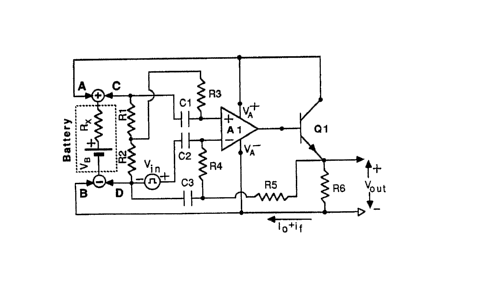
Referrlng next to Flg. 2, a slmplltled schematlc dlagram ot a
sectlon of the block dlagram of Flg. l ls dlsclosed. Operatlonal
25 amplltler Al along wlth its dc blaslng reslstors Rl, R2, and R3, and
1~30164
translstor Ql connected as an em~tter followerl comprlse hlgh-galn
ampl lf ler cascade l 2 of Flg. l . In addltlon, reslstors R4 and R5
along wlth capacitor C3 comprlse low pass fllter l 8; reslstor R6
comprlses reslstlve network 22; and capacltors C l and C2 comprlse
capacltlve coupllng network 38. Battery 24 ls represented ~n Flg. 2
5 by lts equlvalent clrcult comprlslng a battery emf VB ln serles wlth
an lnternal battery reslstance Rx. The perlodlc square-wave slgnal
presented to summatlon clrcultry 26 ~y osclllator 32 at output 30 o~
reslstlve attenuator 34 ls represented by voltage Vln ln flg. 2.
Summatlon clrcultry 26 comprlses the sertes lnterconnectlon o~
voltage Vin and the voltage developed across battery 24 as sensed by
the two connecttons C and D contactlng battery 24.
Stlll reterrlng to flg. 2, dc blas condltlons wlll tlrst be
derlved. The dc blas voltage at the nonlnvertlng (~) lnput ot
operatlonal amplltler Al ls establlshed by the voltage dlvlslon
15 between reslstors Rl and R2. The lnput lmpedance o~ operatlonal
ampll-ler Al can be assumed to be much larger than reslstance R3.
Under such circumstances, the dc voltage across R3 ls negllglble and
the dc voltage at the nonlnvertlng lnput, measured wlth respect to
the negatlve termlnal of the battery, ls equal to
V0 (R 1 ~R2) ( l )
Res~stors R4 and R5 provide an lnternal dc reedback path ~rom
the emltter ot al to the lnvertlng (-) lnput ot Al. The resultlng
~3016~
negatlve dC ~eedback along wlth the very hlgh galn of the ampll~ler
cascade causes the lnvertlng (-) lnput of Al to assume the same dc
blas voltage as the nonlnvertlng (+) lnput. By agaln assumlng the
lnput lmpedance ot operatlonal ampllfler Al to ~e very large, one
tlnds that vlrtually no voltage drop occurs across reslstors R4 and
5 R5. Accordlngly, the emltter o~ Ql assumes the same dc blas
voltage as the lnvertlng lnput o~ Al. The dc component of the output
voltage ls there~ore
Vout(dc) - V0 (Rl~R2) (2)
The dC blas analysls carrled out above shows that translstor
Ql operates as a class-A emltter tollower amplltler and has a dc
blas current glven ~y
o, Vout (dc) , V~ R2 (3)
R6 (R l ~R2)R6
In addltlon to the dc blas component glven by equatlon (2), the
output voltage VWt atso contalns an ac slgnal component. The low-
pass ftlter comprlsed of C3, R4 and R5 effectlvely attenuates ac
20 output slgnals and prevents them frorn passlng through the lnternal
dc feedback path. Accordlngly, the ac component of the output slgnal
wlll be essentlally determlned by the negatlve teedback pl~ovlded by
the external ~eedback c~rcuit.
Referrtng agaln to Flg. 2, one sees thàt an ac current
16
1~0~64
proportlonal to the ac slgnal component of Vout ls passed through the
~attery by means of an ac feed~ack-current 10QP comprlslng
translstor Q 1, reslstor R6, battery reslstance Rx, and conductors
leadlng to battery contacts at A and B. Thls ac teedback current ls
equal to
VOut (ac) (4)
The resultlng ac slgnal voltage developed across the battery
o reslstance Rx ls (lf Rx)~ Thls ac voltage ls sensed at battery
contacts C and D and added ln serles to the ac slgnal voltage Vln
dertved trom the square-wave osclllator output. The composlte ac
slgnal voltage ls then capacltlvely-coupled to the dltterentlal lnput
ot Al by means ot the two coupllng capacltors Ct and C2.
The lnput voltage-senslng loop comprlses battery reslstance
Rx along wlth ac slgnal voltage V~n, capacltors Cl and C2, the
dltterentlal lnput ot operatlonal amplltler Al, and conductors
leadlng to ~attery contacts at C and D. One sees that the lnput
voltage-senslng loop and the output feed~ack-current loop are
20 separate trom one another ~ut are coupled together ~y virtue ot thelr
one shared element -- the battery reslstance Rx.
In vlew o~ the ac negatlve feed~ack and the very large ac galn
of the biased amplltler cascade, the total ac slgnal voltage applted
to the dlfferentlal lnput of operatlonal ampllfler Al ls essentlally
25 zero. Hence, the ac slghal voltage developed across Rx ls very nearly
17
1~0164
equal ln magnttude, but opposlte ln slgn) to the applled ac slgnal
voltage Vln. Accordlngly, one can wrlte
lf Rx ~ ~Vln (S)
5 Comblnlng equatlons (4) and (5) and solvlng tor VOut(ac) leads
to
VOut(ac) = ~ (R6 Vln ) Gx (6)
where G~ ls the battery's dynamlc conductance measured ln
Slemens
One sees from the ac analysls carrled out a~ove that the
5 magnltude ot the ac slgnal component at the output ot the clrcult
dlsclosed ln Flg. 2 ls dlrectly proport10nal to the dynamlc
conductance, Gx, ot the battery 24 undergolng test.
Flg. 2 dlscloses that the battery testlng apparatus makes tour
separate connectlons to the battery 24 undergotng test. Two of
20 these connectlons, at A and C, lndependently contact the posltlve (~)
termlnal ot ~attery 24. The other two connectlons, at B and D,
lndependently contact the negatlve (-) termlnal. Thls speclal four-
conductor contactlng arrangement constltutes "~our-polnt probe"
archltecture. Its purpose ls to effectlvely lsolate the output
25 feedbac~-current loop trom the lnput voltage-senslng loop except
18
016A
ror t~e deslred coupllng provlded by the one shared element, Rx. The
"four-polnt probe" archltecture descrl~ed hereln ls a solutlon to the
severe measurement problem that results trom the tact that the
lnternal reslstance ot a typlcal automotlve-type battery ls
extremely small (- 0.005 ohms) compared wlth the spurlous
s reslstance of pract~cal battery contacts and connectlng wlres --
whlch often total several ohms. In practtce, "four-polnt probe"
connectlons to the battery may slmply comprlse temporary
connectlons lmplemented wlth speclal two-conductor sprlng cllps of
the type dlsclosed ln U.S. Patent ~,873,911.
o As ls dlsclosed above, the ac teedback current lf passes
through the battery by means o~ the "tour-polnt pro~e~ contacts at A
and B. Equatlon (4) dlscloses that the value ot current lf ls
determlned completely by the ratlo ot VOut(ac) to R6. Accordlngly,
several ohms o~ addltlonal spurlous reslstance lntroduced lnto the
15 teedback-current loop by the leads and contacts at A and B wlll not
alter the relatlonshlp between lf and VOut(ac) and wlll theretore not
e~tect measurement accuracy. As ls turther dlsclosed above, the ac
feedback voltage developed across the battery ls lndependently
sensed at "four-polnt probe~ contacts C and D. Slnce the lmpedance
20 of the ampllfler's lnput circult ls of the order of many thousands of
ohms, a few ohms of addltlonal spurlous reslstance ln the lnput
voltage-senslng loop at contacts C an D wlll llkewlse nave
negllglble effect on the measurements. If, however, contact were
made to elther battery termlnal at a slngle contact polnt, any
25 spurlous contact reslstance and lead wlre reslstance would be
19
3016~
common to ~ot~ the teed-~ack current loop and the voltage-senslng
loop and would there~ore add dlrectly to the measured value of Rx
One sees that the "four-polnt pro~e" archltecture descrlbed
a~ove separates the spurlous elements o~ the feedback-current loop
from the voltage-senslng loop thUs perrnlttlng accurate ~attery
5 conductance measurements to be obtalned even though the
lnterconnecttng leads and contacts may themselves have resistances
that are l~undreds of tlmes larger than the battery's lnternal
reslstance, Rx However, ln order tor such ~our-polnt probe"
archltecture to ~unctlon ettectlvely, a very hlgh degree o~ clrcult
lsolatlon must exlst between the teedback-current loop and the
voltage-senslng loop Otherw~se, spurlous slgnal voltages developed
across the spurlous reslstances ln the feedback-current loop --
voltages that are usually many tlmes larger than the mlcrovolt-slze
ac slgnal developed across Rx -- wlll be coupled lnto the voltage-
15 senslng loop and degrade measurement accuracy
For many battery testlng appllcatlons, lt ls very advantageousto power the battery testlng apparatus by the battery undergotng
test rather than requlre, lt to have lts own source o~ power In the
clrcult dlsclosed ~n Flg 2, operational amplifler Al recelves lts
20 operatlng power from the battery undergoing test through power
termlnal VA+~ connected to battery contact A, and power termlnal
VA-. connected to battery contact 8 Slnce "rour-polnt probe"
archltecture places translstor Ql In contact wlth the ~eedback-
current loop, the A and B contacts are used to power Al ln flg 2
25 Thls cho~ce ls dlctated by the lnherent coupllng that exlsts between
1~301~i4
Al and Ql along wlth the need for lsolatlng the feedback-current
loop lrrom the voltage-senslng loop.
"Four-polnt probe" archltecture places the oscillator slgnal Vln
ln the voltage-senslng loop. for a practlcal transtormerless
osclllator clrcult, the osclllator~s output voltage ls establlshed wlth
respect to one o~ lts power supply termlnals. Thus, the cholce of
~attery contacts to be used for powerlng the osclllator wlll be
strongly lnfluenced by the need to provlde adequate clrcult lsolatlon
between the feedback-current loop and the voltage-senslng loop.
Reterrlng next to Flg. ~, a schematlc dlagram slmllar to Flg. 2
ls dlsclosed lncludlng connectlons used for provldlng osclllator
power accordlng to the teachlngs ~ound ln U.S. Patents ~,87~,91 1
and 3,909,708. The ac slgnal Vln ls seen to ~e establlshed between a
slngle osclllator output termlnal and the osclllator clrcult's power
supply termlnal, V0-. Thus, one o~ the osclllator's power supply
termlnals ls also one ot lts output slgnal termlnals and must
there~ore be ln contact wlth the voltage-senslng loop. Accordlngly,
to avold coupllng the voltage-senslng loop to the ~eedback-current
loop, the osclllator ln Flg. ~ recelves lts power through the voltage-
- senslng contacts at C and D.
Powerlng the osclllator c~rcult by means of the voltage-
senslng contacts has two disadvantages. Flrst, because of the very
large ac ampllfler galn, signal levels ln the voltage-senslng loop are
very small. Consequently, excess nolse generated by currents
flowlng through the voltage-senslng contacts, lead wlres, and lnput
clrcultry lntroduces serlous measurement problems. Second,
0i64
practlcal MSI lntegrated clrcults, such as dual and quad operatlonal
amplltlers, do not provlde separate pln-outs tor lndlvldual elements
on the chlp. Theretore, lf the osclllator ls to share ~lSI ICs wlth the
ampllfler and detector, lt must ~e capable of belng powered from the
same palr of battery contacts as the other actlve devlces.
Referrlng now to Flg. 4, a method ls dlsclosed for ln~ectlng a
slgnal lnto the voltage-senslng loop ~y an osclllator powered rrom
contacts ln the feed~ack-current loop wlthout lntroduclng excesslve
loop coupllng. The osclllator of Flg. 4 develops an ac voltage Vosc
between a slngle output termlnal and lts negatlve power supply
o termlnal VO- . The clrcult ls powered by connectlons rom the
osclllator's VO~ and VO- power termlnals to the A and B ~attery
contacts, respectlvely. Thls places the osclllator's power termlnals
dlrectly ln parallel wlth the power termlnals tor tt~e hlgh-galn
ampllfler cascade, VA~ and VA-.
The osclllator ln~ects a slgnal Vln lnto the voltage senslng
loop ~y means o~ lnJectlon reslstor R7 and voltage-vlewlng reslstor
R8. The slgnal current passlng through reslstors R7 and R8 returns
to the VO~ termlnal ot the osclllator ~y passlng through the D
contact and connectlng wlre, through the negatlve battery termlnal
20 ltself, and then through the B contact and connectlng wlre. Thus,
the spurlous reslstances ot the B and D contacts and connectlng
wlres wlll tend to couple the two loops and may therefore degrade
measurement accuracy. However, as wlll be shown more clearly
~elow, lf the osclllator voltage Vos, ls made sufflclently large, the
25 two loops can be lsolated to such a degree that the errors lntroduced
01~4
by spurlous reslstances as large as several ohms wlll ~e negllglble.
Reterrlng next to Flg. 5, a slmpllfled schematlc dlagram ls
dlsclosed whlch wlll now be employed to analyze measurement
errors resultlng trom loop-coupllng tntroduced by the slgnal
ln~ectlon clrcult ot Flg. 4. The tour reslstances RA, Rg, Rc, and RD ln
5 Flg. S represent the spurlous reslstances ot the tour lead-wlres and
contacts at A, B, C, and D, respectlvely. As seen ln Flg. 5, the ac
feed~acl~ current lf passlng through reslstor R6 spllts lnto two
currents, lg and lD. Current lg passes through spurlous reslstance
RB and enters the negatlve termlnal o~ the battery at contact B.
o Current lD passes through the osclllator clrcult, through reslstors
R7 and R8, through spurlous reslstance RD, and enters the negatlve
termlnal ot the battery at contact D. The two currents add together
ln the battery. Thelr sum, lf, leaves the battery at contact A, passes
through spurlous reslstance RA, and returns to the collector ot
15 tranS1StOr Q 1 .
By uslng an approprlate spllttlng tactor derlved trom the
reslstances ot the two paths, one can show that the current lD ls
proportlonal to lf and glven by
[R7~R8 R3;RD~ (7)
The total slgnal voltage at the dltterentlal lnput to the
operatlonal ampllfler ls found by superposltlon of the voltage drops
1~801~4
ln the voltage-senslng loop due to the currents lf and lD, and the
voltage Vln ln~ected lnto the voltage-senslng loop ~y the osclllator.
By vlrtue ot the very large ac galn, thls total ~nput s~gnal voltage ls
essentlally zero. Thus, one can wrlte
[R7 ~ R8 ~ R B ~ RD ~
Ellmlnatlng lD ~rom equatlons (7) and (8) and uslng equatlon (4)
to express lf ln terms ot VOut(ac) leads to
v0ut(ac) - R6 ( R8 ~ RD )
Vosc Rx (R7~R8~RB~RD)~RB(R8~RD)
Equatlon (9) ~an be stmplltled by notlng that reslstors R7 and
R8 are much larger than spurlous reslstances RB and RD. Thus, one
can assume that
R7 RB 1 (tO)
R8 RD J
Accordlngly, equat)on (9) can be wrltten
24
~Oi6
Vout(ac) - R6 R8
( 1 1 )
vosc Rx (R7 ~ R8) + RB R8
Equatlon ( 1 1 ) ls the deslred result. It relates vout(ac) to Vasc
and lncludes the effects o~ both the battery~s lnternal reslstance,
Rx, and the spurlous lead-wlre and contact reslstance, Rg. Note that
only one ot the tour spurlous reslstances wlll have a slgnltlcant
et~ect on the measurernents. Under the assumptlon that
Rx (R7 ~ R8) ~ > RB R8 ( 12)
the second term ln the denomtnator o~ equatlon ( 1 1), the error term,
can be neglected ln comparlson wlth the ~lrst term. Under these
clrcumstances, equatlon ( 1 1 ) becomes
Vout(aC) = r R8 ] [R6 ]
Vosc L R7 ~ R8 Rx
whlch agrees wlth the earlter result glven ~y equatlon (6) slnce
Vln = R7 R8 Vsc ( 14)
Substltutlng equatlon ( 13) lnto lnequallty ( 12) ylelds the
~: 25
~ , ' , " ~'; .
~30164
followlng suttlclent condltlon for neglectlng the error term ln the
denomlnator ot equatlon ( l l ):
V~sc ¦ R6 RB ( I S)
Vout(aC)
s
In the practlcal electronlc ~attery testlng devlce dlsclosed
hereln below, the tollowlng approxlmate values apply:
V ~
o Vout(ac) - l volt
R6 - 20 ohms
Theretore, the magnltude ot the lett-hand slde ot lnequallty (lS) can
be approxlmated ~y
Vout(ac) ¦ ( l 6)
The error term of equatlon ( l l ) lntroduces only a one percent
measurement error when the left-hand slde ot lnequallty (15) ls lO0
tlmes larger than the rlght-hand slde. Therefore, a spurlous
reslstance RB Ot one ohm or less wlll lntroduce a measurement error
that does not exceed one percent . Furtherrnore, the error analysls
above shows that the measurements are une~tected by spurlous
: 25
26
,
1~01~
reststances RA and Rc; and are also uneffected by RD as long as
lnequallty (10) ls satlsfled. Thus, for the osclllator slgnal ln~ectlon
method dlsclosed ln Flg. 4, only the spurlous reslstance RB causes
any potentlal degradatlon of measurement accuracy. ~loreover, as ls
clearly shown by the analysls above, even the deleterlous effect of
5 RB can be effect~vely nulllfled wlth thls clrcult by chooslng V~sc to
be sul'flclently large.
The osclllator clrcult produces a square wave output slgnal at
a frequency of approxlmately 100 Hz. Although the exact frequency
of osclllatlon ls not crltlcal, equatlon ( 1 1 ) dlscloses that VOut(ac) ls
o dlrectly proportional to VOsc. Thus, for hlgh accuracy, the magnltude
ot the osclllator slgnal mwst remaln very constant under all
cond~tlons o~ voltage and temperature encountered ~n operatlon.
The second lnvent~on embodlment dlsclosed ln U.S. Patent
3,873,911 utlllzes an osclllator clrcult comprls~ng a dlscrete
5 operatlonal ampl~fler connected as a conventlonal astable
multlvlbrator. The problems wlth uslng thls clrcult, and stlll
attalnlng the hlgh measurement accuracy deslred ror the present
lnventlon, are twofold. Flrst, the level ot the osclllator's output
slgnal ls nearly proportlonal to lts supply voltage. Thus, wlth
20 osclllator power supplled by the battery belng tested, the accuracy
ot conductance measurements ls very dependent upon the "surface
charge" condltlons of the battery. Second, because of lmperfectlons
that are always present ln the output clrcults o~ IC operatlonal
ampllflers, the saturated maxlmum and mlnlmum output voltage
25 levels are lnevlta~ly otfset ~rom the power supply voltage levels,
27
~30i6~
VO+ and VO-, ~y slgnlflcant amounts that depend on temperature. As
a consequence, the osclllator's output slgnal level changes wlth
temperature, thus lntroduclng a slgnlflcant temperature-dependent
measurement error.
The second lnventlon embodlment dlsclosed ln U.S. Patent
3,909,708 utlllzes a dlfferent type of osclllator clrcult ln an
attempt to solve the problems descrlbed above. Instead of an
operatlonal ampll~ler, the clrcult employes two dlscrete translstors
functlonlng ln a conventlonal astable translstor mult~vlbrator. Thls
tends to ellmlnate the problem of the temperature-dependent output
slgnal level that Is lnherent to IC operatlonal ampllfler
multlvlbrators. In addltlon, the voltage supplled to the
multlvlbrator ls regulated wlth a zener dlode Thls holds the
osclllator's supply voltage, and hence lts output voltage, constant
and tends to reduce the dependence of the measurements ~n the
15 battery's "surface charge".
Ne~ther of the problem solutlons employed ln U.S. Patent
3,909,708 can be employed wlth the present lnventlon, however. The
use of dlscrete translstors ls, o- course, the antlthesls of utlllzlng
~1SI technology. Moreover, wlth ~1SI technology, lt ls not posslble to
20 separately regulate the power supplled to the osclllator slnce all
actlve devlces ln the IC must recelve power from the same source.
Referrlng now to Flg. 6, a schematlc dlagram of an osclllator
clrcult for produclng a preclsely-leveled output slgnal ln accordance
wlth the present lnventlon ls dlsclosed. Operatlonal ampl~er A2
25 along w~th res~stors R9, R 1 O, R 1 1, R 12 and capacltor C4 comprlse a
30~4
conventlonal astable multlvlbrator clrcult. Posltlve feedback ls
provl~ed by reslstor R 12 along wlth voltage dlvlder reslstors R9 and
RtO. Negatlve feedback ls provlded by reslstor Rl 1 along wlth
capacltor C4. As ls well known to one of ordlnary sklll ln the artl
the output voltage of operatlonal ampllfler A2 alternately assumes a
5 maxlmum value near lts posltlve supply voltage, VA~, and a mlnlmum
value near lts negatlve supply voltage, VA-. If R9 and R10 are equal,
the output wavetorm of thls osclllatlon ls nearly symmetr~cal wtth
an osclllatlon perlod, T, glven by
T= (2Rll C4)1n{l~RR2 } (17)
The synchronlzlng output o~ the astable multlvlbrator, Vs~c, ls
connected to the control lnput o~ a C~10S bllateral analog switch Sl.
5 One o~ the slgnal termlnals ot analog swltch 51 ls held at a constant
voltage, Vz, by a zener dlode Dl wh~ch ls supplled power through
serles reslstor R 13. The other slgnal termlnal ot S 1 ls connected to
one slde ot an output load reslstor R 14 whose other slde ls
connected to the negatlve termlnal of dlode Dl. The osclllator
20 output slgnal, VOsc, ls developed across the output load reslstor R 14.
The operatlonal ampllfler power termlnals, VA+ and VA-, are
connected ln parallel wlth the analog swltch power termlnals, Vs~
and Vs~, and toget~er comprlse the osclllator power supply
termlnals, VO~ and VO-, of Flg 4. These common power connectlons
25 recelve power trom the battery undergolng test by means ot
tee~ack-current loop connectlons at battery contacts A and B,
respecttvely. As ls shown ln Flg. 6, the negatlve slde of the
common-mode output slgnal voltage, vosc~ ls ln common wlth power
termlnal VO- and hence wlth battery contact B.
Durlng the portlon Tl of tlme perlod T that the multlvl~rator
5 output ls at lts hlghest level, VSync(hl)~ the analog switch Sl ls
turned "on"~ Assumlng that the "on" reslstance of Sl ls much less
than Rl4, the output voltage then assumes lts hlghest value
Vosc(hl)~vz . (l8)
Durlng the portlon T2 O~ tlme perlod T that the multlvlbrator output
ls at lts lowest level, VS~C(1O)~ the analog swltch S 1 ls turned "o~t".
Assumlng that the "otf" reslstance of S l ls much larger than R l 4,
the output voltage ls essentlally pulled to zero by Rl4 so that
V0sc(lo) ~ O . ( l 9)
Accordlngly, the osclllator output voltage slgnal, Voec~ osclllates
between Vz and zero and very closely approxlmates a per~ectly-
20 leveled square wave havlng a constant peak-to-peak amplltude, Vz.
One sees from equatlon (13) that the peak-to-peak amplltude
of the ac signal component at the output of the hlgh-galn amplltler
cascade ln Flg. 4 ls theretore
301~4
I V ( ~ I [ R8 ~ [ R6] V (20)
The zener dlode voltage, Vz, ls chosen to ~e 5. ~ volts to take
advantage ot the very nearly zero temperature coertlc~ent that ls
5 characterlstlc ot zener dlodes havlng thls partlcular zener voltage.
Accordlngly, lVwt(ac)l wlll ~e very nearly lndependent ot both
battery voltage and lnstrument temperature.
One sees that tt~e slmple preclsely-leveled osclllator clrcult
dlsclosed ln Flg. 6 has propertles tnat are very nearly ~deal tor
appllcatlon ln an electronlc ~attery testlng devlce. It can be
powered from common power supply connectlons and dellvers a
preclse output slgnal level that ls vlrtually lndependent ot ~Oth
temperature and supply voltage. These speclal attrlbutes ot the
slmple clrcult dlsclosed ln Flg. 6 contrlbute to the very hlgh
15 measure~ent accuracy t~at ls ac~leved wlt~ tne lnventlon nereor.
Reterrlng next to Flg. 7, a scnematlC dlagram ot a slrnple, yet
very accurate, sync~ronous detector clrcult ln accordance wlth the
present lnvent~on ls dlsclosed. The purpose ot thls clrcult ls to
provlde a dc output slgnal, Vd~t, that ls preclsely proportlonal to the
20 peak-to-peak amplltude or the ac slgnal component ot the
amplltler's output voltage, IVOu~(ac)I, whlle totally lgnorlng the dc
~las component, Vout(dc)~ A partlcular teature ot the clrcult ot Flg. 7
ls that lt ls vlrtually unresponslve to spurlous slgnal components,
SUCh as ac hum and nolsej that are uncorrelated wlth t~e osclllator
2 5
31
.
,~ ;'.
,
~01~'~
slgnal, Vogc The synchronous detector clrcuit thus permlts
operatlon ot the battery testlng devlce ln electrlcally "nolsy~'
envlronments wlthout requlrlng the extenslve use ot shleldlng --
WhlCh would substantlally lncrease manufacturlng costs. As ln the
case ot the osclllator clrcult dlsclosed above, the s~mchronous
detector clrcult dlsclosed hereln ls capable ot belng powered trom a
common source dellverlng power contlnuously to other actlve
elements ln the clrcult. It ls theretore tully compatlble wlth
modern t~151 IC technology.
The clrcult ot Flg. 7 dlscloses a C~OS bllateral analog swltch
o S2 and operat~onal amplifler A3 along with reslstors R15, R16, R17,
and capacltors C5 and C6. Operatlonal amplltler A~ along wlth
reslstors R15, R17, and capacltor C6 comprtse an lntegrator clrcult.
The nonlnvertlng (~) lnput ot A 3 ls blased to the value ot the dc
component ot Vout by means o- reslstor R 16 along wlth bypass
15 capacltor C5. The slgnal applled-to the lnvertlng (-) lnput ot A3 ls
derlved rrom Vout and passes through reslstor R15 and analog SWltCh
52. Thls slgnal ls swltched "on" and "ott" at the osclllator trequency
by vlrtue ot the synchronlzatlon slgnal, VSync~ that ls obtalned trom
the clrcult ot Flg. 6 and applled to the control lnput of S2.
Just as ln the case of the osclllator clrcult dlsclosed Flg. 6,
both the operatlonal ampllfler and the analog swltch of the detector
clrcult ot Flg. 7 are powered through common connectlons to the
feedback-current loop battery contacts at A and B. Both ot the two
lnput slgna~s dlsclosed ln the clrcult ot Flg. 7, VO~Jt and Vsync~ are
25 common-mode slgnals establlshed wlth respect to the negatlve
32
1~ ~3O1~L~
power supply lead contactlng the battery at B.
Operatlon of the synchronous detector clrcult of flg. 7 wlll
now be explalned by means of reterence to the tlmlng and wave~orm
dlagrams o~ Flgs. 8a, 8b, 8c, and 8d.
Flg. 8a lllustrates the wavetorm of the common-mode Yoltage,
Vout~ developed across reslstor R6 o~ the clrcult o~ Flg. 4 and applled
to the slgnal lnput of the clrcult of Flg. 7. By vlrtùe of the 180
degree phase lnverslon performed by the hlgh-galn ampllfler cascade
o~ Flg. 4, Vout assumes lts low value Vout(lo) durlng t~me- perlod Tl
for whlch V0SC ls h~gh, and lts hlgh value VoUt(hl) durlng tlme perlod
T2 for whlch Vosc ls low. Vout thererore osclllates about lts dc blas
value Vout(dc) ~ V0 glven by equatlon (2). The peak-to-peak value ot
the ac component o~ Vout ls seen to be
¦Vout(aC)¦ = {Vout(hl)--Vout(dc)} + ~VOut (dc)--vOut(lo)l (21 )
Because o~ the ac coupllng provlded by coupllng capacltors Cl
and C2 at the lnput ot ampll~ler Al, the average excurslons ot Vout
above and below lts dc blas value are equal. Accordlngly, the two
shaded areas o~ Flg. 8a can be equated to yleld
{VoUt(dc)--Vout(l)}Tl = {Vout(hl)--Vout(dC)}T2 (22)
33
1~30~64
Su~stltut~ng equatlon (22) lnto equation (21 ) ylelds
¦Vout(aC)l = [ lT 2 ] [Vout(dc) -Vout(lo)l (2~)
Flg 8b lllustrates the waveform of the synchronlzatlon slgnal,
YS~nC~ developed at the output of operatlonal amplltler A2 ln Flg 6
and applled to the synchronlzatlon lnput of the clrcult of Flg 7 Thls
common-mode voltage slgnal osclllates between two voltage levels,
VS~"c(hl) and VS~nc(lo)~ at the osclllator frequency of approxlmately
100 Hz The perlod ot the osclllatlon T~ ls there~ore
approxlmately lOmllllseconds
Now conslder the clrcult ot Flg 7 ln greater detall For
slmpllclty, assume lnltlally that lntegratlon capacltor C6 ls zero
The negatlve ~eedback provlded ~y reslstor R17 along wlth the hlgh
galn ot operatlonal ampll~ler A3 ensures that the voltage at the
lnvertlng (-) lnput ot A3 wlll be very nearly the same as the voltage
at the nonlnvertlng (~) lnput 8ecause o~ the low-pass ~llterlng
actlon of blas reslstor R16 and bypass capacltor C5, the voltage at
the nonlnvertlng lnput, measured wlth respect to the negatlve power
20 supply termlnal VA-, ls slmply the dc blas component of the lnput
voltage, Vout(dc)~ Therefore, the voltage at the lnvertlng (-) lnput ls
llkewlse Vout(dc)~
Durlng tlme lnterval Tl, analog swltch S2 ls turned "on" by
synchronlzatlon slgnal Vs~nc(hl) Dur~ng thls lnterval, operatlonal
25 ampllfler A~ serves as a slmple lnvertlng ampllfler wlth lnput
34
~ ,
1~30164
s~gnal Vout - vout(lo) and output slgnal Vd~t = Vd~t(hi). A feedback
current ls tlows through reslstor R l 7, through swltch S2, and
through reslstor Rl5 as shown ln Flg. 7. Assumlng that the "on"
reslstance ot S2 ls small compared wlth RtS, one can wrlte thls
current ln terms of the voltage drop across elther Rl5 or Rl7 as
5 follows:
s = {Vout(dC)--V0ut(lo)} = Vdet(hl) (24)
o Comblning equatlons (23) and (24) leads to
det [Tl tT2 ~ [ Rl53 1 out ¦ , (25)
Equatlon (25) detlnes the hlgh output level Vd~(hl) seen ln Flg. 8c.
Durlng tlme lnterval T2) analog swltch S2 ls turned "o~" by
synchronlzatlon slgnal VS~ o)~ Assumlng that the "or~" reslstance
of S2 ls su~lclently large, one can assume that ls~ 0 so that no
20 voltage drop exlsts across Rl7. Accordlngly, the output o~ A3
assumes the same voltage, Vout(dc)~ that exlsts at both the lnvertlng
input and the noninvertlng lnput of A3. Since the output voltage
equals the voltage at the nonlnvertlng lnput, Vd~t ls zero. Thls zero
value def~nes the low output level seen ln Flg. 8c.
Flg. 8c lllustrates the waveform ot the dl~terentlal-mode
1~3016~
output slgnal of the synchronous detector. One sees from the
analysls detalled above that the output voltage ,Vd~, osclllates
between the hlgh value Vd~t(hl), glven by equatlon (25), and zero. The
average, or dc value of Vd~t, ls therefore
r Tj
det LT1 +T2 ~ det . (26)
Comblnlng equatlons (25) and (26) to ellmlnate Vd~t(hl) leads to
[~T~ I T2) ] [ 5 ]
The ettect of lntroduclng the lntegrat~on capacltor C6 lnto the
15 clrcult ot Flg. 7 ls lllustrated ln Flg. 8d. One sees that the average
value of the detector output slgnal, Vd~(dc), ls uneftected by C6.
However, the lntegratlon capacltor smooths the varlatlons ln output
voltage about the average value, thus reduclng the rlpple component
of Vd~t. For a suttlclently large value of lntegratlon capacltor C6,
20 Vd~t ls slmply equal to Vd~t(dC)
Equatlon (27) shows that the dc slgnal voltage at the
dlfferentlal output of the synchronous detector ls dlrectly
proportlonal to the common-mode ac slgnal component at the output
of the hlgh-galn ampllfler. The analysls above dlscloses that the
25 constant of proportlonallty is not e~tected by ampll~ler galn or
36
1 ~3016~
osc~llator frequency. The relationshlp between VOut(ac) and Vd~t
depends only upon the ratlo of two reslstance values, R l 5 and R l 7,
and the osclllator symmetry ratlo (Tl/T2). Futhermore, lt ls very
lnsenslt~ve to changes ln the symmetry ratlo when Tl and T2 are
nearly equal. Thus, the detector clrcult dlsclosed ln Flg. 7 has
5 nearly ldeal characterlstlcs for appllcatlon to the accurate
determlnatlon of battery conductance.
Moreover, the dlrect proportlonallty descrlbed by equatlon (27)
only occurs tor slgnal components whlch are at the osclllator's
exact frequency and are fully correlated wlth the osclllator slgnal.
All other slgnals, such as spurlous ac hum and nolse, wlll not
contrlbute to the average value o~ Vd~ and wlll therefore be
et~ectlvely removed trom the detector's output s~gnal by the
smoothlng e~rect o~ the lntegratlon capacltor, C6. The clrcult
dlsclosed ln F~g. 7 thus permlts obtalnlng very accurate battery
15 measurements ln electrlcally "nolsy" envlronments wlthout
requlrlng that the testlng devlce be extenslvely shlelded and
therefore expenslve to manu~acture. Important economlc bene~lts
can consequently be galned throug~ the use o~ the synchronous
detector clrcult dlsclosed ln Flg 7 ln a practlcal battery testlng
20 devlce. Furthermore, ~n contrast to the detector clrcult dlsclosed
ln U.S. Patent ~,909,708 whlch requlres "chopped" dc power, the
clrcult o~ Flg. 7 has no speclal power source requlrements and ls
fully compatlble wlth modern MSI IC technology.
Referrlng next to Fig. 9, a schematlc dlagram o~ a slmple
25 ad~ustable dc ampll~ler and output meterlng clrcult ln accordance
37
30i6~
wlth the present inventlon ls dlsclosed The clrcult comprlses only
operatlonal ampllfler A4, dc mllllameter mA, and varlable resistor
Rl8 Iust as ln the case o~ all the other actlve devices, operatlonal
ampllf~er A4 recelves lts dc power from common connectlons to the
~attery at the feedback-current loop contacts A and B
S The nonlnvertlng t+) lnput of operatlonal ampll~ler A4 ls
connected to the nonlnvertlng (~) lnput of operatlonal ampllfler A~
ot Flg 7 by the negatlve slgnal lead of Vd~t Accordlngly, the
nonlnvertlng lnput of A4 lS blased to the same dc level, Vout(dc)~ as
the nonlnvertlng lnput o~ A3 By vlrtue o~ the negatlve feedback
o lntroduced by the slgnal path through mllllameter mA, along wlth
the hlgh galn of operatlonal ampll~ler A4, the lnvertlng (-) lnput of
amplltler A4 assumes the same voltage level as the nonlnvertlng
lnput The entlre dlt~erentlal lnput slgnal, Vd~t, theretore appears
across the lnput reslstor R l 8 Slnce the current through the
15 mllllameter, Im, ls the same as the current through lnput reslstor
R l 8, the meter current can be slmply calcu1ated by applylng Ohm's
law to R t 8 The dc meter current ls theretore
m R l 8 (28)
One sees that the slmple clrcult dlsclosed ln Flg 9 provldes a
dc current Im through the mllllameter that ls directly proportlonal
' to VdBt(dc) The constant of proportlonallty relat~ng Im to Vdeffdc) ls
seen to be lndependent o~ the meter's lnternal reslstance and ls
25 determlned completely by the value o~ the lnput reslstor Rl8
Oi64
Equatlons (20), (27) and (28) can now be comblned to derive a
slngle relatlonshtp relatlng the meter current, Im, to the osclllator's
zener voltage, Vz, ~or the enttre electronlc battery testlng devlce
dlsclosed ln the ~lock dlagram o~ Flg. 1. The resultlng equatlon ls
wr~tten
Im = r Tl T2 lr R6 R8 R17 1 Gx (29)
VZ ~T1 +T2)2JL(R7 ~ R8) R15 R18 J
Equatlon (29) conflrms that the dc meter current ls dlrectly
proportlonal to the battery's lnternal conductance Gx. ~oreover, the
constant of proportlonallty ls slmply and preclsely determlned by
the value ot Vz along wlth slx reslstances and the symmetry ratlo,
(Tl/T2) . In practlce, (Tl/T2) ls very nearly one. Thus,
Im 1 r R6R8R17
Gx (30)
Vz 4 (R7~R8)Rt5R18
By uslng flxed reslstances and callbratlng the dc mllllameter
ln unlts proportlonal to lnternal conductance, such as cold-cranklng
amperes or ampere-hours, tne disclosed ~attery testlng devlce will
emulate a dlrect readlng devlce of the type dlsclosed ln U.S. Patent
3,8731911. It wlll be apparent to one skllled ln the art that ln such
an appllcatlon, the dc ampllfler and mllllameter could be replaced
by any llnear dlsplay devlce, Such as a dlgltal meter, that ls capable
. . .
0~64
of provldlng a numerical dlsplay proportlonal to V~et(dc).
Alternatlvely, by lettlng one of the six resistances be a
varlable reslstance, callbratlng lt ln battery ratlng unlts such as
cold-cranklng amperes or ampere-hours, and then arranglng
mllllameter mA to deslgnate simple qualltatlve condltlons, the
5 dlsclosed devlce wlll emulate a "pass-fall" battery testlng devlce of
the type dlsclosed ln U. S. Patent 3,909,708. It wlll ~e apparent to
one skllled ln the art that ln such an appllcatlon, the mllllameter
could be replaced by a varlety ot dlsplay means, such as colored
llghts, that are capable ot lndlcatlng the qualltatlve condltlons.
o Moreover, lt can be seen rrom equatlon (~0) that lt Im ls
brought to a partlcular tlxed value, such as the "pass-~all" polnt, by
ad~ustlng one ot the reslstances ln the denomlnator -- R15 or Rl~
(or R7 under the condltlon R7 R8) -- the approprlate value ot the
varlable reslstance wlll be dlrectly proportlonal to the battery's
15 conductance Gx. Hence, lt varlable reslstance R18 ln Flg. 9 has a
llnear taper, lt can be llnearly callbrated ln conventlonal battery
ratlng unlts -- such as ampere-hours or cold cranklng amperes --
that are proportlonal to the conductance of a ~attery capable ot
deltverlng lts full-rated power. Such ltnearlty of the ratlng scale
20 tmproves preclslon and Is a great convenlence for the operator.
Flg 10 dlscloses a complete schematlc dlagram of an Improved
devlce for testlng 1 2-volt automotlve batterles ln accordance wlth
the present lnventlon. Operatlonal amplltlers 100, 102, 104, and
106 comprlse four elements of an r1Sl quad operatlonal ampl~ler
25 lntegrated clrcult, ICl. Bllateral analog swltches 108 and 110
~0164
comprlse two elements of a cr10s bllateral swltch lntegrated
circutt, IC2. Both ICl and IC2 are powered by means of common
connectlons, l l 2 and l l 4, to the battery undergolng test 24 through
current-~eedback loop contacts l 16 and l l8, respectlvely.
Hlgh-galn ampllfler cascade 12 or flg. l comprlses operatl.onal
s amplltler tO0 and npn translstor 120 connected as an emltter
follower. Reslstor l22 conducts a dc blas voltage to the
nonlnvertlng (~) lnput of operatlonal amplltler lO0 trom voltage
dlvlder reslstors l 24 and l 26 whlch are connected to battery 24
through voltage-senslng contacts l 28 and l 30. The output voltage
ot hlgh-galn amplltler cascade l 2 ls establlshed across external-
path reedback reslstor 22. An lnternal feedback path comprlslng
reslstors l ~2 and l 34 conducts the dc voltage at the common
connectlon between the emltter of npn translstor 120 and reslstor
22 to the lnvertlng (-) lnput of operatlonal ampllrler l O0 . Reslstors
l 32 and l ~4 along wlth capacltor l ~6 comprlse low-pass rllter l 8
ot Flg. l .
The ac slgnal voltage developed across ~attery 24 ls sensed at
voltage-senslng contacts l 28 and l ~0 and added ln serles to an
lnput signal voltage component establlshed across vlewlng reslstor
20 l~8. The resultant composlte ac slgnal voltage ls applled to the
dlfferentlal lnput of operatlonal ampllfler lO0 by a capacltlve
coupllng network comprlslng capacltors 140 and l42 A feedback
current that ls proportlonal to the voltage establlshed across
reslstor 22 passes through battery 24 by means or external teedback
25 path conductors 144 and l 46 along wlth cu~rent-tee~ack loop
41
l~t ~301~4
battery contacts 1 16 and 1 18.
The ac lnput slgnal voltage establlshed across vlewlng
reslstor 138 ls generated by a preclsely-leveled osclllator clrcult
comprlslng operatlonal ampllfler 102, analog swltch 108, and zener
dlode 148. Operatlonal ampllfler 102 along wlth reslstors 150, 152,
154, 156, and capacltor 158 comprlse a conventlonal astable
rnultlvlbrator clrcult used to generate a square-wave synchronlzlng
slgnal. Reslstor 160 supplles blas current to zener dlode 148. The
synchronlzlng output of operatlonal ampllfler 102 connects to the
control lnput of analog swltch 108. The two slgnal contacts o~
o analog swltch 108 lnterconnect the output of zener dlode 148 wlth
the lnput o~ potentlometer 162. Potentlometer 162 provldes means
to lnltlally ad~ust the level of the voltage slgnal outputted by analog
swltch 1 08
SPST swltch 164 provldes ~or the selectlon ot elther o~ two
levels o~ slgnal voltage and serves as a temperature compensatlon
adJustment. Thls temperature compensatlon ad~ustment corrects
for ~attery temperature and provldes means for obtalnlng lncreased
accuracy when measurlng batterles at other than room temperature.
Wlth SPST swltch 164 tn the open posltlon, a current proportlonal to
20 the output voltage of potentlometer 162 passes through In~ectlon
reslstor 166 and ls ln~ected lnto vlewlng reslstor 138 thereby
developlng a slgnal voltage across vlewlng reslstor 1~8 Closure o~
swltch 164placesreslstor 1681nparallelwlthreslstor 166
thereby ~ncreaslng the level of stgnal voltage developed across
25 vlewlng reslstor I 38; as would be approprlate to measurlng a
42
1.2~0~64
battery that was at a reduced temperature It will be apparent to
one of ordlnary sklll in the art that several alternatlve temperature
compensatlon methods are avallable For example, the ternperature
compensatlon ad~ustment could provlde more than two slgnal values;
or lt could be lmplemented wlth a conttnuous, rather than a dlscrete,
5 reslstance ad~ustment In addltlon, a temperature compensatlon
ad~ustment could be lmplemented by varylng reslstances at other
locatlons ln the battery tester clrcult as can be easlly recognlzed
from an examlnatlon of equatton (~0) derlved hereln above
Analog swltch 1 10 along wlth operat~onal ampllfler 104,
o whlch ls connected as an lntegrator, comprlse synchronous detector
clrcu~t 40 ot Flg 1 Reslstor 170 and ~ypass capacltor 172
comprlse a low-pass tllter wh~ch blases the non~nvertlng lnputs ot
operatlonal amplitlers 104 and 106 to the voltage level of the dc
blas component developed across reslstor 22 A slgnal current
15 derlved trom the total voltage at the common connectlon between
reslstor 22 and translstor 120 passes through reslstor 174 and
analog swltch 1 10 to the lnvertlng lnput ot operatlonal ampllfler
104 Th~s slgnal current ls perlod~cally lnterrupted at the osclllator
frequency by vlrtue of the control lnput of analog swltch 1 10 belng
20 connected to the synchronlzlng output of operatlonal amplifler 102
Reslstor 176 prov~des negatlve dc feed~ack to operatlonal ampllfler
104 Integrat~on capacltor 178 serves to smooth the detected
voltage signal outputted by operatlonal ampllfler 104
A current derlved from the detected slgnal voltage at the
25 output of operat~onal amplltler 104 passes throug~ mllllameter 180
~0164
to the output of operatlonal ampllfler 106 by way of one of the two
paths selected by SPDT swltch 182 Wlth swltch t80 ln posltlon 1,
the meter current passes through flxed reststor 184 Under these
condltlons, the dlsclosed lnventlon emulates a dlrect readlng battery
testlng devlce havlng an output lndlcatlon that ls proportlonal to the
5 dynamlc conductance of battery 24 Wlth swltch 182 ln posltlon 2,
the meter current passes through flxed reslstor 186 and varlable
reslstor 188 Under these condltlons the dlsclosed lnventlon
emulates a "pass-fall" battery testlng devlce havlng an ad~ustable
~attery ratlng scale that ls llnearly related to the settlng of
10 varlable reslstance 188 and a ratlng of ~set that ls determlned by the
value or tlxed reslstor 186 As wlll be apparent to one of ordlnary
sklll ln the art, several alternatlve llnear battery ratlng adJustment
methods can be lmplemented As dlscussed hereln above, a llnear
relatlonshlp wlll exlst between battery ratlng and the ad~ustment
15 reslstance lr any one ot the three reslstances ln the denomlnator o~
equatlon (30) ls chosen to be the ad~ustment Thus, one could choose
to select and vary reslstor 174 tR15) lnstead of reslstor 188 (R18)
Alternatlvely, lf reslstor 168 was not employed for temperature
compensatlon, one could choose to vary reslstor 166 (R7) under the
20 condltlon that the lnJectlon reslstor 166 ls much larger than the
vlewlng reslstor 138 (R8)
A 11st of component types and values for the lmproved
electronlc battery testlng devlce dlsclosed ln Flg 10 follows
44
30~6L~
REFERENCE NUMBER ~2MPONENT
$emtconductor Dev1ces
100,102,104,106 ICl - L~324N
108,110 I C2 - CD4066B
120 TIP~lC Power Transistor
148 1 N52~ 1 B Zener Dlode
S Reslstors - Ohms (1 /4-W unless s~ecltled)
22 22 - 5 Watts
138,186 100
184
188 500 Varla~le
124,126,160 lK
162 5K Trlmpot
122,176 47K
lC 170,174 1 OOK
154 1 50K
156 270K
166 330K
132,134,1 50,1 52 t l~leg
168 1.5 Meg
Ca~ac1tors - 1'1td
158 0.022
136,140,142, 172 0.47
178 1 0
~Jleter
180 1 mA dc mllllameter
2G Although a speclfic mode for carrylng out the present
lnventlon has been hereln described, it ls to ~e understood that
mad~flcatlon and varlatlon may be made without departlng from
what ls regarded to be the sub~ect matter of the lnventlon. For
example, vlsual dlsplay means have been speclflcally dlsclosed
4S
: ~ `
1~301~4
nerein above. However, the output of the disc~osed electronic
battery testing circuit could alternatively be monitored by a voltage
senslng devlce that responds to a drop in output slgnal level by
soundlng an audlble alarm, causing a visible display, or by switching
partlcular equlpment to an alternative power source. I~loreover, the
5 clrcult output could be monltored ~y a computer speclflcally
programmed to respond appropriately to the level of the output
slgnal. The range of potential computer responses would be
virtually unllmlted and is restricted only by the imaginatlon of the
computer progammer. These, and other varlatlons are belleved to be
o well withln the scope of the inventlon and are lntended to be covered
~y the appended clalms.
46