Note: Descriptions are shown in the official language in which they were submitted.
1~80180
NONLINEAR SIGNAL GENERATING CIRCUIT AND
NONLINEAR COMPENSATING DEVICE USING THE SAME
BACKGROUND OF THE INVENTION
The present invention relates to a device for compensating
for nonlinearity of amplifiers by use of a predistortion principle
and a nonlinear signal generating circuit using such a device~
5 More particularly, the present invention is concerned with a
nonlinear compensating device of the type using a distortion
generating circuit in which diodes are built in to serve as
distortion generating elements~
Heretofore, a nonlinear signal generating circuit of the kind
I0 described has been imPlemented with a circulator~ Specifically,
a circulator is provided with a reflection port in addition to an
input and an output pors Connected between the reflection port
and ground is a parallel connection of two parallel diodes ~hich
are connected with polarities opposite to each other and a
15 terminating resistor which is parallel to the diodes~ The diodes
serve as nonlinear elements~ A radio frequency ~RF) signal
coming in through the input port is terminated by such a parallel
circuit so that only nonlinear components generated by the
diodes appear on the output port. A drawback with this kind of
20 nonlinear signal generating circuit is that the bandwidth available
'
l~olsn
is determined by that of the circulator and, therefore, cannot be
~ide enough as desired. Another drawback is that a magnet
which is necessarily included in the circulator makes it difficult to
implement the construction with a planar circuit and, thereby,
5 obstructs the implementation of the circuit with a microwave
integrated circuit. In addition, circulators having the same
impedance are difficult to produce without adjustment and this,
too, obstructs the implementation of the circuit with a
microwave integration circuit~
On the other hand, a prior art nonlinear compensating
device in which the above-described nonlinear signal generating
circuit is installed to serve as a tistortion generating circuit
includes a po~er distributor, or power splitter, havin~ an input
terminal and a power combiner having an output terminal~ An
15 input signal is divided by the power distributor into t~o signals~
One of the two signals is fed to the power combiner over a
nonlinear route which includes the distortion generating circuit
and a variable attenuator connected in series with the distortion
generating circuit~ The other signal is applied to the power
20 combiner over a linear route which includes a delaY line and a
variable phase shifter connected in series with the delay line~
The two signals delivered through the linear and nonlinear routes
are combined by the power combiner in opposite phase and,
then, fed out via the output porS Such a prior art nonlinear
2 5 compensating device has some problems left unsolved~
1~30:18~
--3--
Specifically, since the linear and nonlinear routes lack
symmetry, the phase difference between them has dependence
upon frequency preventing the nonlinear compensating device
from being provided with a wide bandwidth~ In addition, since
5 the individual structural elements are fabricated independently of
es.ch other and connected together by connectors and cables,
difficulty is experienced in uniformizing the characteristics due to
scattering in characteristic and others which are ascribable to
the connection~
SUMMARY OF TIIE INVENTION
It is, therefore, an object of the present invention to provide
a nonlinear signal generating circuit operable over a wide
bandwidth.
It is another obiect of the present invention to provide a
nonlinear signal generating circuit which can be implemented with
a planar circuit and, therefore, with a microwave integrated
circuit.
It is another obiect of the present invention to Pro~ide a
20 nonlinear signal generating circuit which eliminates the need for
ad justment~
It is another object of the present invention to provide a
nonlinear compensating device with high wide band performance.
It is another obiect of the present invention to provide a
2 5 nonlinear compensating device which eliminates scattering in
1280180
-4--
characteristic due to the connection of individual structural
elemenS, thereby promoting uniformization of characteristics.
In accordance with the present invention, a nonlinear signal
generating circuit comprises a quadrature hybrid having an input
5 port, a coupling port, a passing port and an output port, a
first parallel connection constituted by a first and a second diode
which are connected in parallel and opposite in polarity to each
other and a first terminating resistor which is connected in
parallel with the first and second diodes, the first parallel
10 connection being connected at one end to the coupling port OI the
quadrature hybrid and at the other end to ground, and a second
parallel connection constituted by a third and a fourth diode
which are connected in parallel and opposite in polarity to each
other and a second terminating resistor which is connected in
15 parallel with the third and fourth diodes, the second parallel
connection being connected at one end to the passing port of the
quadrature h~rid and at the other end to ground~
~ urther, in accordance with the present in~ention, a
nonlinear compensating device comprises a power distributor
20 constituted by an input terminal and a first quadrature hybrid, a
distortion generator constituted by a second quadrature hYbrid
and nonlinear elements and connected to the power distributor, a
variable attenuator constituted by a third quadrature hybrid and
PIN diodes and connected to the distortion generatin~ circuit, a
25 fixed phase shifter constituted by a fourth quadrature hybrid and
~;~80180
--5--
propagation lines and connected to the power distributor, a
variable phase shifter constituted by a fifth quadrature hybrid
and varactor diodes and connected to the fixed phase shifter,
and a power combiner constituted by a sixth quadrature hybrid
and an outPut terminal and connected to the variable attenuator
and variable phase shifter.
BRIEF DESt~RIPTION OF THE DRAWINGS
The above and other objects, features and advantages of the
present invention will become more apparent from the following
detailed description taken with the accompanYing drawings in
which:
Fig~ 1 is a diagram schematically showing a prior art
nonlinear signal generating circuit of the type using a circulator;
Fig. 2 is a schematic diagram showing one embodiment of a
nonlinear signal generating circuit in accordance with the present
invention;
Fig~ 3 is a schematic blocX diagram showing a prior art
nonlinear compensating device;
2 0 Fig~ 4 is a schematic blocX diagram sho~lring a nonlinear
compensating deYice in accordance with the present invention;
and
Fig~ 5 is a perspective view showing the device of Fig~ 5
which is constructed into a microwave integrated circuit.
l~ao~so
--6--
DESCRIPTION OF THE PREFERRED EMBODIMENIS
Referring to Fig~ 1 of the drawings, a prior art nonlinear
signal generating circuit 10 includes a circulator 12 which has an
input port 14, a reflection port 16, and an output port 18.
5 Two diodes 20 and 22 are connected in parallel and opposite in
polarity to each other to serve as nonlinear elements~ A
terminating resistor 24 is connected in parallel to the diodes 20
and 22. The parallel connection made up of the diodes 20 and
22 and terminating resistor 24 is connected at one end to the
10 re~lection port 16 and at the other end to ground. An RF signal
coming in throu~h the input port 14 is terminated by the parallel
circuit so that o~ nonl~ear components generated by the two
diodes 20 and 22 are fed to the output port 18. With this prior
art circuit 10 with the circulator 12, it is difficult to increase the
15 bandv~idth and to implement the circuit 10 with a microwave
integrated circuit, as previously discussed.
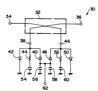
Referring to Fig. 2, a nonlinear signal generating circuit
embodying the present in~ention is shown and generally
designated by the re~erence numeral 30. As shown, the circuit
20 30 includes a quadrature hybrid 32 as its maior comPonent.
The quadrature hybrid 32 has an input port 34, an isolation
port 36 which serves as an output port, a coupling port 38 to
which two diodes 40 and 42 and a terminal resistor 44 are
connected, and a passing port 46 to which two diodes 48 and 50
25 and a terminating resistor 52 are connected. The diodes 40 and
i~30180
--7--
42 are connected in parallel and opposite in polarity to each
other, and so are done the diodes 43 and 50. With respect to
high frequency, the diodes 40 and 48 and the terminal resistors
44 and 52 are connected to ground by bypass capacitors 54, 56,
58 and 60, respectively. On the other hand, the diodes 42 and
50 are conn~cted to ground directly. A bias terminal 62 is
provided at the iunction of the diodes 40 and 48 and bypass
capacitors 56 and 58, allowing a bias current to be fed to the
four diodes 40, 42, 48 and 50 therethrough. In this
construction, a high frequency signal applied to the input port
34 is diYided to reach the coupling port 38 on one hand and the
~assing port 4 6 on the other hand. The signal reached the
couplin~ port 38 is terminated by the diodes 40 and 42 and
terminating resistor 44 ~hile the other signal reached the passing
port 46 is terminated by the diodes 48 and 50 and terminating
resistor 5 2. As a result, only nonlinar signals which are
individually generated by the diodes 40 and 42 and the diodes 48
and 50 are combined by the quadrature hybrid 3~, a composite
signal appearing on ~he output port 36.
2 0 The nonlinar signal generating circuit 3 0 having the above
construction is advantageously operable over a wide bandwidth
because its major element is the quadrature hybrid 3 2. The
quadrature hybrid 32 can readily be implemented with a planar
circuit and, therefore, allows the circuit 30 to be fabricated in a
25 microwave integrated circuit confi~uration. In addition, the
1~80180
--8--
quadrature hybrid 32 eliminates the need for adjustment.
Referring to Fig. 3, there is shown a prior art nonlinear
compensating device 70 which uses the prior art nonlinear signal
generating circuit lO of the type using a circulator as shown in
5 Fig. 1 for a distortion generating circuit. As shown, the
compensating device 70 includes a powcr distributor 72 having
an input terminal 74 and two output terminals 72a and 72b, and
a power combiner 76 having an output terminal 78 and two input
terminals 76a a~d 76b. The output terminal 72a of the power
lO distributor 72 is connected to the input port 14 of the distortion
~enerating circuit 10 via a connecting line 80. The output port
18 of the distortion enerating circuit lO is connected to an inp~t
terminal 86 of a variable attenuator 84 the output terminal 88 of
which is connected to the input terminal 76a of the po~er
1~ combi~er,6 by a line 9G. The path extending from the output
terminal 72a of the power distributor 72 to the input terminal
76a of the po~er combiner 76 via the line 80, distortion
generating circuit 10, line 82 and Yariable attenuator 84
constitutes a nonlinear route. The other outPut termi~al 72b of
20 the power distributor 72 is connected to an input terminal 96 of
a variable phase shifter 94 by a delay line 92~ An output
terminal 98 of the variable phase shiîter 94 is connected to the
input terminal 76b of the power combiner 76 by a line 100. The
path extending from the output terminal 72b of the power
25 distributor 74 to the other input terminal 76b of the power
~2~30180
g
combiner ~6 via the delay line 92, variable phase shifter 94 and
line 100 constitutes a linear routQ An inPut signal applied to
the input terminal 74 of the power distributor 72 is divided into
two signals one of which is propagated through the nonlinear
5 route and the other through the linear route~ The power
combiner 76 combines the two signals in opposite polaritY and,
therl, deli~ers the resulting composite signal via the output
terminal 7 8~ This kind of prior art compensating circuit is
limited in wide band performance and suffers from scattering in
10 characteristic, as stated earlier.
Referring to Fig. 4, a nonlinear compensatin~ de~ice in
acco. dance ~ith the present in~ ention is shown which is free
from the drawbacks discussed above. As shown, the
compensating device, generally 110, includes six quadrature
hybrids 112, 114, 116, 118, 120 and 122 which are identical in
distributed constant line. The first quadrature hybrid 112 is
conllected to an input terminal 12 6 and ser~es as a power
distributor 124. One of two output terminals of the power
distributor 124 is connected to a distortion generating circuit 128
20 ~hich is identical with the distortion generating circuit shown in
Fig. 2 except for a DC biasing circuit and the bypass capacitors
5 4 to 6 0 . The circuit 12 8 is constituted by the second
quadrature hybrid 114 and two parallel connections 130 and 132
connected to the hybrid 1 14~ The parallet connection 130 is
made up of dlodes 134 and 136 and a terminal 138 connected in
12801~0
- 1 o--
plarallel with the diodes 134 and 136 while the parallel connection
132 is made up of diodes 140 and 142 and a terminating resistor
144 connected in parallel with the diodes 140 and 142. The
diodes 134 and 136 are connected in parallel in opposite relation
5 to each other with respect to polarity, and so are done the
diodes 140 and 142, each diode serving as a nonlinear element.
Connected to the distortion generating circuit 128 is a variable
attenuator 146 which is constituted by the third quadrature
hybrid 116 and two PIN diodes 148 and 150. A DC biasing
circuit for these diodes 148 and 150 is not shown in Fig~ 4. The
~ariable attenuator 146 is connected to a po~er combiner 152
which is constituted by the sixth ~uadrature hybrid 12" and
provided with an output terminal 154. In this manner. the
distortion generating circuit 128 and variable attenuator 146 are
1~ cascaded between the po~er distributor 124 and power combiner
152 to set up a nonlinear route.
A fixed phase shifter 156 is made up OI the fourth
quadrature hybrid 118 and two distributed constant lines 158
and 160. The fixed phase shifter 156 is connected to the other
20 output terminal of the power distributor 124 and to a variable
phase shifter 162 which consists of the fifth quadrature hybrid
120 and two Yaractor diodes 164 an 166. A DC biasin~ circuit
for these varactor diodes is not shown in Fig. 4. With respect
to a variable phase shifter of this type, a reference may be made
to U. S. Patent 4,638, 269 issued January 20, 1987. The
~28018~
variable phase shifter 162 is connected to the power combiner
152. As stated, the fixed phase shifter 156 and variable phase
shifter 162 are cascaded between the power distributor 124 and
the power combiner 152 to complete a linear route which is
5 symmetrical to the previously mentioned nonlinear route.
Signals propagated through the two routes are combined in
oppositc phase by the power combiner 152 so that a composite
signal appears on the output terminal 154.
As shown in Fig. 5, the diodes 134, 136, 140 and 142, the
resistors 138 and 144, the PI~I diodes 148 and 150, and
~aractor diodes 164 and 166 which are built in the compensating
de~ice 110 are used in pair ch.ps without exception. Further, all
the quadrature hybrids 112. 114, 116. 118, 120 and 122 are
provided in patterns (microstrip lines) on a single dielectric
15 substrate 168 together with their associated connecting lines and
fixed phase shifter 156. All the circuits are accommodated in a
sin~ie air-tight housing 170 to complete a microwaYe integrated
circuit. Such a configuration allows a minimum scattering due
to connection and scattering in characteristic due to unnecessary
20 reactance to occur, whereby characteristics are uniformalized~
In addition, by ~irtue of the symmetry established between the
nonlinear and linear routes, i. e., the identical phase
characteristic of the two routes, the frequency-dependence of the
phase difference between the two routes is effectively reduced to
25 allow the frequency band to be broadend as desired.
)180
--12--
In summary, it will be seen that a nonlinear signal
generating circuit of the present invention exhibits desirable wide
band performance, can be implemented with a planar circuit
and, therefore, with a microwave integrated circuit with ease,
5 and eliminates the need for adjustment. All these advantages
are derived from the use of a quadrature hybrid.
Further, a nonlinear compensating device of the present
invention achieves a wide bandwidth as well as uniform
characteristics because it uses the combination of quadrature
10 hybrids and various kinds of diodes, and because they are
provided on a single dielectric substrate and accommodated in a
single air-tigbt ~o1ssing with symmetry of the circuit preserved.
Various msdifications will become possible for those skiMed
in the art after, eceiving tbe teachings of tbe present disclosure
15 withsut departing from the scope thereof.