Language selection

Search

Patent 1280477 Summary

Third-party information liability

Some of the information on this Web page has been provided by external sources. The Government of Canada is not responsible for the accuracy, reliability or currency of the information supplied by external sources. Users wishing to rely upon this information should consult directly with the source of the information. Content provided by external sources is not subject to official languages, privacy and accessibility requirements.

Claims and Abstract availability

Any discrepancies in the text and image of the Claims and Abstract are due to differing posting times. Text of the Claims and Abstract are posted:

  • At the time the application is open to public inspection;
  • At the time of issue of the patent (grant).
(12) Patent: (11) CA 1280477
(21) Application Number: 547522
(54) English Title: HIGH DENSITY FLEX CONNECTOR SYSTEM
(54) French Title: CONNECTEUR SOUPLE HAUTE DENSITE
Status: Deemed expired
Bibliographic Data
(52) Canadian Patent Classification (CPC):
  • 339/108
  • 339/11.3
(51) International Patent Classification (IPC):
  • H05K 3/36 (2006.01)
(72) Inventors :
  • ELCO, RICHARD A. (United States of America)
  • VANDEGRIFF, HUGH R. (United States of America)
(73) Owners :
  • ELCO, RICHARD A. (Not Available)
  • VANDEGRIFF, HUGH R. (Not Available)
  • E. I. DU PONT DE NEMOURS AND COMPANY (United States of America)
(71) Applicants :
(74) Agent: MCCALLUM, BROOKS & CO.
(74) Associate agent:
(45) Issued: 1991-02-19
(22) Filed Date: 1987-09-22
Availability of licence: N/A
(25) Language of filing: English

Patent Cooperation Treaty (PCT): No

(30) Application Priority Data:
Application No. Country/Territory Date
911,679 United States of America 1986-09-26

Abstracts

English Abstract


TITLE
High Density Flex Connector System
Abstract of the Disclosure
Photodefined pin and guide arrangements on a
connector and a printed wiring board are used to obtain an
alignment between the connector and the printed wiring
board. A clamp fixed to the connector housing squeezes
the connector contact fingers to the connector pads of the
board to engage pads and fingers which have been guided
into an overlapping position by the guide and pin
arrangement.


Claims

Note: Claims are shown in the official language in which they were submitted.


Claims
1. In a system for connecting a photodefined
array of connector pads on a printed wiring board with a
matching array of photodefined connector contact fingers
and squeezing the connector into contact with the printed
wiring board that includes a squeeze clamp for the
connector and the printed wiring board, means for aligning
said contact fingers as the connector fingers are guided
into an overlapping position with said pads within said
clamp comprising: a photodefined first guide located at
each side of the array of connector pads; and a
photodefined second guide located at each side of the
array of fingers, said first and second guides
intermeshing as said connector fingers are guided into
said overlapping position to precisely align said fingers
with said pads.
2. The system of Claim 1 wherein said first
guides are shaped like a vee-block and said second guides
are shaped like a wedge to fit together with the
vee-block.
3. The system of Claim 1, including a third
slotted guide located at the leading edge of the connector
at each side of the array of fingers and a pin mounted on
said printed wiring board on each side of the array of
said pads, said pins engaging said slotted guides to
approximately align said first and second guides.
4. The system of Claim 3 wherein said third
guide is photodefined on said connector.


Description

Note: Descriptions are shown in the official language in which they were submitted.


TITLE
High Density Flex Connector System
Background of the Invention
This invention is directed to the alignment of a
connector to a printed wirin~ board (PWB).
The preparation and alignment of connectors to a
PWB has been generally carried out by a complex, exacting
process u6ing the PWB edges for po6itioning the ~onnector
fingers relative to the PWB contact pads. The known
10 positioning ~ystems are not capable of positioning
connector on center~ of much less than 50 mils. A system
has been developed for reducing the complexity and
incre~ing the reliability of the alignment of such
connections.
Su~mary of the Invention
Thi6 invention provides a high density flex
connector system capable of accurate alignment of the
connector fingers with pads of a printed wiring board.
The mean6 for alignment includes a photodefined fir6t
guide located at ~ach 6ide of an array of pads located at
the ends of traces of a printed wiring board and a
photodeined second guide located at each side of an array
of connector fingers at the ends of traces on a flex
connector. The first and second guides intermesh ~s
connector ~inger~ are guided into an overlapping position
with the pads to preci6ely align the fingers with pads.
Similarly, meshing guides located ~lightly ahead of said
first and ~econd guides and with greater longitudinal
and lateral travel during meshing than the first and
second guides to provide a coarse alignment pr;or to
~e~hing o~ the fir6t and 6econd guides.
Brief Description of the Drawin~s
Fig. 1 i~ a perspective view of a connection
~ystem that utilizes the invention.
~iq. 2 is a ~ectioned view of Fig. 1 taken along
line 2-2.
'~


Fi~. 3 is a sectioned view of Fig. 1 taken along
line 3-3.
Fig. 4 is an enlarged view of a portion of Fig.
3.
Fig. 5 is an enlarged partial plan view of the
overlap connection between the PWB and the flex connector.
Fig. 6 i~ an enlarged partial view of Fig. 5.
Detailed Description of the Preferred ~mbodiment
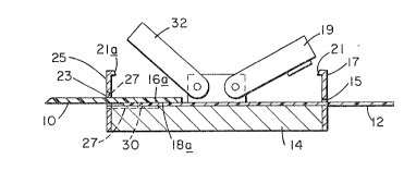
Referring now to Fig. 1, the embodiment chosen
for purpose~ of illustration includes a printed wiring .
board 10 and a flex connector 12 joined together in ~n
overlapping relationship within clamping connector housing
~4. The overlapping relationship i~ best ~hown in Fig6.
2, 5 and 6 wherein PNB lO and flex connector 12 have
photodefined trace~ 16, 16 respectively applied to opposed
~urfac~s 16a, lBa in a manner well known in the art. The
traces 16 terminate in an array of connector pads 20 while
the traces 18 terminate in an array of fingers 22. The
means for aligning the PWB with the flex connector
includes guide arrangements attached both to the Pws and
the flex connector. More particularly, referring to Fig.
5 vee-shaped fir6t guides 26 are located at each side of
the array of connector pads 20 on PWB 10 and wedged-shaped
second guides 24 are located at each side of the array of
fingers 22 of the flex connector 12. The guide~ 24, 26
are photodefined at the time the trace~, pad6 and finger~
are photodefined, i.e., all in one operation. In addition
to guides 24, 26 ~lotted third guides 2B are located at
each ~ide of the array of fingers 22 on the flex connector
12 at its leading edge 12a. These guides ~8 have a ~lot
28a in them to accept an alignment pin 30 mounted at each
6ide of the array of pad~ 20 on PW~ 10. The guides 28 are
photodefined on connector 12 while pin~ 30 are made of
~teel and are inserted in holes on PW~ 10. ~uid~s 28 and


3 ~ 3~717
pins 30 form a coarse alignment arrangement to bring
guides 24, 26 to approximate alignment before they mesh to
provide precise alignment of the fingPrs 22 with the pads
20. Since the pads ~nd fingers overlap, the guides 24, 26
are plated to a thickness of the overlap so they will
engage as the PWB overlap the flex connector in housing
14. Electrical traces 31,32 located on flex connector 12
and PWB 10 respectively provide an electrical path to the
edges of the flex connector and PWB to enable
electroplating up of the guides 24,26,28. In addition
these trace~ provide vertical po~itioning of the flex
connector relative to the P~B during the joining procsss
60 that the fingers 22 properly overlap the pads 20.
The ho~ing 14 i6 used to 6queeze PWB lO and
flex connector 12 together to make contact between pad~ ~0
and fingers 22. Flexible connector 12 enters hou~ing 14
through a ~lot 15 in end wall 17 of the housing and is
clamped in place by pivoting lever 19 which locks in place
under a lip 21 of wall 17. The PWB enters housing 14
through a ~lot 23 in end wall 25 of the housing. Slot 23
has enlargements 27 to allow pins 30 on PWB lO to pass
through. When the Pws is in position overlapping
connector 12 as 6hown with ~urfaces 16a, l~a facing each
other, a pivoting lever 32 squeezes them together to make
contact between the pads 20 and fingers 22. The lever
lock6 in place under a lip 21a of wall 2S.
Since the alignment quides 24, 26 and the traces
wi~h fingers and pads on the connector and PWB are
photodefined in one operation, an absolute positioning
reference ~y~tem i~ establi~hed which permit~ po itioning
o~ c~nnector pad~ on much clo6er centers on the PW~ than
previou~ly po~ible.

3~


Representative Drawing
A single figure which represents the drawing illustrating the invention.
Administrative Status

For a clearer understanding of the status of the application/patent presented on this page, the site Disclaimer , as well as the definitions for Patent , Administrative Status , Maintenance Fee  and Payment History  should be consulted.

Administrative Status

Title Date
Forecasted Issue Date 1991-02-19
(22) Filed 1987-09-22
(45) Issued 1991-02-19
Deemed Expired 1994-08-20

Abandonment History

There is no abandonment history.

Payment History

Fee Type Anniversary Year Due Date Amount Paid Paid Date
Application Fee $0.00 1987-09-22
Registration of a document - section 124 $0.00 1987-12-15
Maintenance Fee - Patent - Old Act 2 1993-02-19 $100.00 1992-12-16
Owners on Record

Note: Records showing the ownership history in alphabetical order.

Current Owners on Record
ELCO, RICHARD A.
VANDEGRIFF, HUGH R.
E. I. DU PONT DE NEMOURS AND COMPANY
Past Owners on Record
None
Past Owners that do not appear in the "Owners on Record" listing will appear in other documentation within the application.
Documents

To view selected files, please enter reCAPTCHA code :


To view images, click a link in the Document Description column. To download the documents, select one or more checkboxes in the first column and then click the "Download Selected in PDF format (Zip Archive)" or the "Download Selected as Single PDF" button.

List of published and non-published patent-specific documents on the CPD .

If you have any difficulty accessing content, you can call the Client Service Centre at 1-866-997-1936 or send them an e-mail at CIPO Client Service Centre.


Document
Description 
Date
(yyyy-mm-dd) 
Number of pages   Size of Image (KB) 
Representative Drawing 2000-07-06 1 8
Drawings 1993-10-15 2 79
Claims 1993-10-15 1 37
Abstract 1993-10-15 1 14
Cover Page 1993-10-15 1 14
Description 1993-10-15 3 139
Fees 1992-12-16 1 82