Note: Descriptions are shown in the official language in which they were submitted.
20365-2690
~ACKGROU~D OF TH~ I~VE~TIO~
In broadband digital signals switching and/or
transmission systems, transit time effects place a limit on the
chronological resolution of the switching and~or -transmission
system and, thexefore, on the maximally-allowable bit rate
which, in the meantime, can be upwardly shifted by time
regeneration of the broadband dlgital signals. This
repetikion, under given conditions, in short, ~hree-dimensional
spacing~ is discussed, for example, in the Ger~an published
application 28 36 6g5 and in the publication Pfannschmidt,
"Arbettægeschwindigkeitsgrenzen von Zeitvielfach-
Raumkoppelnetzwerken fur Breitband-Digitalsignale",
dlssertation, Braunschweig, 1978, partlcularly Page 78. Such
transit time effects thereby stem not only from the short
translt times ~er se which are no longer neyligible and which
add up within the switching and/or transmission system and from
transit time scatters of integrated circuits, but also stem
from the ~act that the signal edges experience a shift due to
crosstalk phenomena. On the contrary, ~he chronological
resolution is also deteriorated in that, in particular, active
circuit elements exhibit different t.ransi~ times for signal
edges having differing signs. The present invention,
proceeding from a coding of the broadband digital signals in a
DC-frae code, then provides a manner by which the latter can be
countered by a time regeneration which involves only little
expense.
SV~HARY OF THE I~V~TIO~
The present invention is directed to a circuit
arranyement for time regeneration of digital signals comprising
a correction circui~ and an appertaining control circuit
containing a low-pass ~ilter. This circuit arrangement,
8~3~
20365-2690
according to the present invention, is particularly
characterized in that, for time regeneration of broadband
digital signals in broadband digital signal switching and/or
transmission syskems which are coded in a DC-free code, a
correction element comprising a digital signal input and a
control input is inserted into the signal path. The digital
signal experiences an increased transit time at its signal
edges o~ one sign and experiences a reduced transit time at the
same time at its signal edges of opposi~e sign in this
lQ correction element, based on the measure of every DC component
occurring in the digital signal. A control circuit identifying
such a DC component comprises a limiter circuit charged by the
digital signal and a low-pass filter circuit following
thereupon leadlng to the control input of the correction
element.
The present invention, which exploits the fact that
freedom from direct current wlth respect to the digital signal
to be transmitted is usually desired by way of a corresponding
coding, offers the advantaye of correction of transit time
differences of the digital signal edges having differing signs
that involves little expense and is partlaulary ef~ective at
the same time and therefore reduces the requirement of more
involved tlme regenerators which are otherwise required.
The known compensa~ion, from the German published
application 33 46 725, of changes of the pulse duty factor of a
phase demodula~ed data signal, moreover, also
20365-2690
requires such a higher expense, in accordance wherewith the
data signal, DC decoupled with a high pass ~ilter, is
regenerated by a comparator at whose one input an invarlable
reference voltage is applied at whose other input a sum signal
of the ph~ase demodulated data signal and an auxiliary signal
holding the DC mean values thereof constant is supplied, this
auxiliary signal being derived in a compensation circuit from
khe output signal of the comparator forming the compensated
data signal by low-pass filtering, integration and inversion.
It should also be mentioned here that it is known in
the context of a scanning of a graphics original~ and
conversion o~ the scan signal into a digital signal to provide
a differentiating network and a high-gain comparator following
the differentiating network in the signal path in order to
achieve a signal detec~ion of small input signal pulses
contained in the background signal which is independent of
variations oi a background signal and/or o~ input signal pulse
amplitude and/or duration, the output of the comparator being
connected to the second input of the first-mentioned
differentiatlng network via a negative feedback path comprising
a limiter, a mean value circuit and a further differentiating
network which has its second input applied to a reference
voltage source (U.S. Patent 4,263,555); no points of closer
contact are established within ~he present invention.
Returning now to the present invention~ the limiter
circuit can precede the correction element in the signal path
in accordance with a further fea~ure of the invention.
Alternatively to such a formation of the circuit
z
20365-2690
arrangement of the present invention, as a control arrangement,
however, is also possible to construct the circuit arrangement
as a regulating arrangement in which the limiter circuit
follows the correction element in the digital signal path or in
which the limiter circuit and correction element forms a single
circuit unit in the diyital signal path.
In accordance with a further feature of the
invention, the correction element can be simply formed with a
threshold circuit having a switching threshold controlled by
the control circuit, whereby the shift of the switchin~
threshold effects the deslred time regeneration in combination
with the finite edge steepness of the broadband digital signal.
A resistor capacitor (RC) element may often suffice
as a low-pass fllter circuit in the control circuit.
In accordance with a further feature of the
invention, the low-pass filter circuit can be connected to the
control input of ~he correction element via a controlled gain
amplifier, whereby the controlled gain amplifier can be
deslgned in view of a proportional (P) or of a proportional-
integrated (PI) control characteristic dependent on therequirement of the arrangement.
According to a broad aspect of the inven~ion there is
provided a circui~ arrangement for time regeneration of digital
signals, comprising:
a correction element for time regeneration of broadband
æignals coded in a DC-free code, comprisiny a digital signal
input and a control input inserted in a signal path;
the digital signal experiencing an increased transi~ time
at its signal edges of one sign in said correction element and
æimultaneously experiencing a reduced transi~ time at its
s:Lgnal edges of the respectively other sign based on ~he
348Z
2036s-26so
measure of each DC component occurring in the digital signal;
a control circuit including a limlter for receiving the
digital signal and a low-pass ~ilter connected to said limiter,
said control circuit identi~ying said DC components, the output
of said control circuit leading to said control input.
BRI~F DESCRIPTIO~ OF THE DRAWINGS
Other objects, features and advantages of the
invention, its organization, construction and operation will be
best understood from the following detailed description, taken
in conjunction with the accompanying drawings, on which:
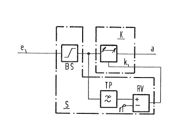
Figure 1 is a schematic representation of an
exemplary embodiment of a control circuit arrangement
constructed in accordance with the present invention;
4a
~L~8~32
20365-2690
FIG. 2 is a schematic representat;.on of an exemplary
embodiment of a regut.ating circuit constructed in accordance
witll the present invention;
FIG. 3 is a ~chematic representation of an exemplary
emboaiment of a regulating circuit constructed in accordance
with the present i.nvention;
FIG. 4 is a schematic representation of an exemplary
embodiment of a regulating circuit con~tructed in accordance
with the pre~ent invention; and
FIG. 5 is a schematic representation of another exemp-
Lary embodiment of a regul.ating circuit constructed in accor-
dance with t1~e present invention.
DESCRIPTION OF THE PREFERRED EMBODIMENTS
ReEerring to FIG. l, an exemplary embodiment of a
ci.rcuit arrangement for a time regeneration of broadband digital
gignal9 i9 illustrated a~ compri~ing a correction element K
inserked into a ~ignal path e-a traver~ed by a broadband digital
signal, the correction element K being prece~ed in the signal
path e-a by a limiter aircuit as of a control circuit S which
al.so comprise~ a low-pas~ fllter TP leading to a control input k
of t1~e correction element l~ and following the limiter circuit BS
charged by the ~igital signals. A controlled gain amplifier RV
having differential input~ + and - whose input (-) can be
assumed to be charged with a reference ~ignal rl i8 inserted
between the low pa~s Eilter TP and the correction element k in
the exemplary embodiment of FIG. l.
As a result of a coding of the broadband digital
signal in a DC~free code, the two signal states "high"
-- 5
~L~8~1~82
20365-2690
and "low" occur for equal lengths in the broadband digital
signal as seen statistically (i.e. over an adequately~long
time). The circuit arrangement of the present invention
exploits this ~haracteristic in order to at least partially
eliminate signal distortions caused by different transit times
of digital signal edges ha~ing differing signs. When the pulse
duty factor of the broadband digital signal appearing at the
signal path inpu~ e or, respectively, stated more precisely, of
the digital signal amplitude-limited in the limiter circuit BS
1~ deviates from the ratio 1,1, i.e. when the signal state "hiqh"
appears for a longer (or, respectively, shorter time) than the
signal state "low" as seen over an adequately-long time, then a
corresponding modification of the output signal of the low-pass
filter TP and, therefore, of the control signal supplied to the
control input k of the correction element K via the controlled
gain amplifier RV arises, on the basis of which the leading
dlgltal slgnal edges experience an increased (or, respectively,
reduced) transit tlme in the correction element K and the
trailing digital signal edges experience a reduced (or,
respectively, increased) transit time in the correction element
K. The deviatlon of the pulse duty factor from the value 1:1
can therefore be largely eliminated for the broadband digital
signal appearing at the signal path output a.
How the correction element K and the limiter BS can
be realised in detail may be seen from the further exemplary
embodiment of a circuit arrangement for time regeneration of
broadband digital signals in accordance with the present
in~ention illustrated in Figure 2. According to
8~
20365-2690
FIG. 2, the correction elemen-t K is formed with a threshold
circuit KS having a switching threshold controlled by the con-
trol circuit S, in particular, comprising a switching transistor
Tk in gate circuitry inserted into the digital signal path e-a
to whose gate electrode the control circuit S is connected and
which has its output connected at a Eeed voltage source UDD
(for example, +5V) via a load transistor Tl. In the exemplary
embodimen-t of FIG. 2, the switching transistor Tk is thereby an
n-channel enhancement field effect transistor and the load
transistor Tl, forming a current source circuit together with
the feed voltage source UDD, is a p--channel enhancement
field effect transistor.
The limiter BS is formed with a complementary-metal-
oxide semiconductor (CMOS) inverter circuit comprising two
transistors Tpb and Tnb. As further indicated in FIG. 2, the
low-pass filter TP can be formed with a simple RC element.
Since, as illustrated in FIG. 2, the low-pass filter TP is con-
nected to the output a of the inverter circu t Tpb, Tnb, the
digi-tal signal inversion eEEected is taken into consideration,
in par-ticular, in tha-t the inputs of the controlled gain ampli-
fier RV, again inserted between the low-pass filter TP and the
correction element control input k, are interchanged with one
another in FIG. 2 in comparison to the conditions illustrated in
FIG. 1.
In the exemplary embodiment o-f FIG. 2, moreover, the
control circuit S follows in the digital path e-a departing Erom
the conditions of the correction element K illustrated in FIG.
1. Instead of the control arrangement of FIG. 1, one therefore
obtains a regulating arrangement in accordance with
~a~2
20365-2690
FIG. 2 comprising the possibility inherent in such an arrange-
ment of being able to arbitrarily precisely correct deviations
of the pulse duty factor from its reference value by way of a
corresponding connection of the controlled gain amplifier RV.
In the time regeneration circuit of FIG. 2, it is
assumed that a potential of, for example, about lV prevails at
the signal path input e, and, therefore, at the digital signal
input of the correction element K in the digital signal state
"high" and a potential of, for example, about 2V prevails at
the digital signal state "low", whereby the two voltage states
should statistically appear for identical lengths, i.e. as seen
over an adequately-long tilne due to a coding of the broadband
digital signal in a DC-free code. Thereby, le-t it be assumed
that a con-trol potential of, for example, about +004V proceeding
from -the control circuit S be applied to the control input k of
the correction element K and, therefore, at the gate elec-trode
oE the switching transistor Tk of the threshold circuit KS,
whereby the switching threshold of the switching transistor Tk
connected to the load transistor Tl may be assumed to lie there-
below by a threshold voltage of, for example, about -1.8V.
Given the signal state "high", the switching transistor Tk in
the threshold circuit KS is then non-conductive and a potential
of about +3.3V in the present example then arises at -the input
-
of the following limiter circuit BS whose switching threshold
can be assumed to lie at about +~V, the p-channel transistor Tpb
of the CMOS inverter BS being non-conductive (or at most very
weakly conductive) due to this potential and the n-channel
transistor Tnb being highly conductive. Given the digital state
3~
20365-2690
"low", the switching transistor Tk and the threshold circuit KS
i9 conductive and a potential of about -1.2V in the present
example arlses at the input of the following limiter BS, the
p-channel transistor Tpb of the CMOS inverter being conductive
due to this potential and the n-channel transistor Tnb being
non-conductive. By way o:E -the low-pass filter TP, the chrono-
logical mean value of the digital signal appearing at -the
limiter output proceeds to the input (-) of the differential
amplifier RV whose other input (+) can be assumed to be charged
with -the reference signals r2 and from whose output it can be
assumed that the control potential of +0.4V in the present
example is output given a pulse duty factor 1:1 observed by the
broadband digi-tal signal.
When the pulse duty actor of the broadband digital
signal deviates :Erom the .Eactor 1:1 , i.e. when the signal state
"high" occurs :Eor a longer (or, respectively, shorter) time than
the signa:L state "low" as seen over an adequately-long -time,
and, consequently, the signal state "low" appears for a longer
(or, respectively, shorter) time than the signal state "high" at
the inverter output a, then a corresponding decrease (or,
respectively, increase) of the ou-tput signal of the low-pass
filter T~ arises as does, therefore, a corresponding increase
(or, respec-tively, decrease) in the input signal difEerence at
the controlled gain ampliEier RV. This causes a corresponding
increase (or, respectively, decrease) in the potential supplied
from the output of -the controlled gain amplifier RV to the
.. control input k of the correction element K of, for example,
0.2V, with the result -that, accordingly, the swi-tching threshold
_ _
20365-2690
of the CMOS threshold circuit KS is increased (or, respectively,
decreased). The leading digital signal edges therefore cross
the switching -threshold later or, respectively, earlier and,
therefore, experience an increase (or, respectively, decrease)
in transit time and the trailing digital signal edges fall
below -the switching threshold earlier (or, respectively, later)
and, therefore, experience a reduced (or respectively,
increased) transi-t time. ~ach deviation of -the pulse duty
factor from the reference value 1:1 can, therefore be eliminated
for the broadband digital signal appearing at the signal path
output a in FIG. 2. As warranted, however, yet another
inver-ter circuit can be followed here in order to, in turn,
cancel the inversion of the broadband digital signal effective
in the limiter BS of FIG. 2.
FIG. 3 illustra-tes an exemplary embodiment of a
circuit arrangement constructed in accordance wlth the present
invent.ion in w'hich t'he co:rrection element is again formed with a
t'hreshold circuit comprising a switching threshold controlled by
a control circuit and the control circuit again comprises a
limi-ter charged by the digital signal and comprises a low-pass
filter TP following the limiter, whereby the limiter and the
correction element now form a single circuit unit in the digital
signal path. The limiter is again an inverter circuit Tpb, Tnb
realized in CMOS technology. A further p-channel transistor Tpk
is inserted between the p-channel transistor Tpb and the
appertaining feed voltage source ~DD and a fur-ther n-channel
transistor Tnk is inserted between -the n-channel -transistor Tnb
and the appertaining voltage sourse Uss. At their control
-- 10 --
4~Z
20365-2690
electrodes, these two further CMOS transistors Tpk and Tnk are
controlled proceeding from a low-pass filter TP, again -formed
with an RC element in accordance with FIG. 3. The signal path
output is re-ferenced a in FIG. 3, wherewith the inversion of the
time regenerated broadband digital signal effected in the inver-
ter circuit Tpb, Tnb can be taken into consideration. As
warranted, however, another inverter circuit can also be
additionally inserted here in order to again cancel the inver-
sion of the broadband digital signals.
When the pulse duty factor of the broadband digital
signal appearing at the signal path input e deviates from the
ratio 1:1, i.e. when the signal state "high`' occurs for a longer
(or, respectively, shorter) -time than the signal state "low" as
seen over an adequately-long time, then a corresponding decrease
~or, respectively, increase) of the output signal of the low-
pass filter Tp and, therefore, of the control potential supplied
via th0 con-trol input k to the two ~urther CMOS transistors Tpk
and Tnk arises, on the basis w~ereoE the channel formation is
facilitated (or, respectively, made more difficult) in the p-
channel transistor Tpk and the channel formation is made more
difficult (or, respectively, facilitated) in the n-channel
transistor Tnk, with the result that the switching threshold of
the CMOS inverter circuit Tpb, Tnb is increased (or, respective-
ly, decreased) accordingly. The digital signal leading edges
therefore cross a switching threshold later (or, respectively,
earlier) and therefore experience an increased (reduced) transit
time and the digital signal -trailing edges Eall below the
-- 11 --
~a~3~82
20365-2690
switc'hing -threshold earlier (or, respectively, later) and there-
fore experience a decreased (or, respectively increased) transit
time.
FIG. 4 illustrates a further exemplary embodiment of
the circuit arrangement for time regenera-tion constructed in
accordance with the presen-t invention and comprising a correc-
tion circuit and limiter constructed as a single circuit unit in
the digital signal path e . In accordance with FIG. 4, a CMOS
inverter Tpbk, Tn'bk inserted in -the signal path e-a is capacit-
ively coupled to the input e for receiving the digital signalwhich is to be chronologically genera-ted. At -the same time, the
inverter input is electrically charged with a switching
threshold controlled voltage by way of a low pass filter TP,
formed as an RC element in accordance with FIG. 4, whereby the
low-pass filter TP is, in turn, charged with the inverted, time
regenerated digital signal. ~et another CMOS inverter Tpi, Tni
is inserted into the actual digital signal e-a following the
output a of the CMOS inverter Tpbk, Tnbk which is directly
connected to t'he input of the low-pass filter TP for this
purpose, this being done in order to cancel the inversion of the
broadband digital signal effected in the correction and limiter
circuit Tpbk, Tnbk. ~s was already set forth above, such an
additional inverter Tpi, Tni can also be provided in the circui-t
arrangements o~ FIGS. 2 and 3. When, in the circuit arrangement
of FIG. 4, the pulse duty factor of the broadband digital signal
appearing at the signal path input e deviates from the ratio 1:1
and when the signal state "high" appears for a longer (or,
respectively, shorter) time than the signal state "low" as seen
- 12 -
32
2036s-26so
over an adequate]y-long time, then a corresponding decrease
(or, respectively, increase) in the output signal of the low-
pa~s fl:Lter TP and, therefore, in the bias electrically supplied
via the contro~ input k to the inverter circuit Tpbk, Tnbk
arises, with the result of a corresponding displacement of the
broadband digital signal which is to be time regenerated and
which is effective at the control electrode o-E the two tran-
sistors Tpbk and Tnbk. The digital signal leading edges there-
fore exceed the switching threshold later (or, respectively,
lO earlier) and therefore experience an increased (or, respect- -
ively, decreased) transi-t time and the digital signal trailing
edges fall below the switching threshold earlier (or, respect-
iveLy, later) and therefore experience a decreased (or, respect-
ively, increased) transit time.
~ ust as in the circuit arrangement of FIG. 3, the
signal emitted at the output by the low-pass filter TP is
directly supplied to the contro:L input k in -the circuit arrange-
ment oE FIG. 4, i.e. foregoing a controlled gain amplifier. The
elimination of a controllecl gain amplifier occurs that only a
P-controlled characteristic is possible, the effect thereof to
be weakly dimensioned in favor of the stability of the control
circuit.
FIG. 5 illustrates a further exemplary embodiment of
the present invention for a circuit arrangement for -time
regeneration of broadband digital signals which likewise
foregoes a controlled gain amplifier. Here, the correction
element is formed with a comparator KK which is inserted into
the digital signal path e-a and to whose reference input (-) a
- 13 -
~a6~
20365-2690
low-pass filter TP Eormed by an RC element and charged with the
outpu-t signal of -the comparator KK leads. For example, the
comparator can be forrned with a simple emit-ter coupled logic
(ECL) element which, as known, has the appearance of a differ-
ential amplifier at i-ts input side, whereby the relatively high
sensitivity established in ECL elements simultaneously provides
the required limiter func-tion.
When, in the circuit arrangement of FIG. 5, the digi-
tal signal s-tate "high" appears at the signaL path input e for a
longer (or, respec-tively, shorter) -time than the signal state
"low", as seen over an adequately-long time, a corresponding
increase tor, respectively, decrease) in the output signal of
the low-pass filter TP and, therefore, in the reference signal
supplied to the reference input t-) oE the comparator KK as well
appears. This effects a corresponding raising tor, respect-
ively, lowering) of the comparator threshold which is therefore
exceeded later tor, respectively, earlier) by the digital signal
leading edges and ls fallen be:low earlier tor~ respectively,
later) by the digital signal trailing edges, wherewith the digi-
tal signal leading edges experience an increased tor, respect-
ively, decreased transit time and the digital signal trailing
edges experience a decreased tor, respectively, increased)
transi-t time.
Although I have described my invention by reference to
particular illustrative embodiments thereof, many changes and
modifications of the invention may become apparent to those
skilled in the art without departing from the spirit and scope
32
20365-2690
of the invention. I therefore intend to include within the
patent warranted hereon all such changes and modifications as
may reasonably and properly be included with the scope of my
contribution to the art.
- 15 -