Note: Descriptions are shown in the official language in which they were submitted.
33
- 1 - 60285-845
POWER LINE COMMUNICATION APPARATUS
BACKGROUND OF THE INVENTION
a. Field of the Invention
This invention broadly relates to digital communications
systems. More speci~ically, it concerns transmitting and receiv-
ing high speed digital lnformation signals in binary form, such as
computer data, over any noisy line medium, such as alternating
current (AC) power lines.
b. Description oE the Prior Art
Digital information, such as computer data, is known to
be capable oE transmission over existing alternating current (AC)
power lines. The potential benefits of such data communication
are well-recognized, including extreme versatility Eor inter-
connecting electronic o~fice products, da-ta terminals, remote
printers, personal computers and the like. Creation of data paths
may be accomplished simply by plugging the dis-tributed terminals
in-to any available AC outlet. Any type of equipment that can be
run by a central computer could be linked to that computer through
the same power cord already provided for such equipment. Such a
central computer could be used to control various process equip-
ment, including heating, lights, and air conditioning.
The presently common situation with the vast majority of
users requiring digital communication lines is the use o-E hard-
wiring to interconnect -the various components. This is expensive,
inflexible, and generally provide higher data
,, .
"f,
33
1 rates than are necessary for the average user. Since AC
power wiring already exists in most, if not all, locations
where data transmission is needed, reliable high-speed
digital communication through this medium would provide
significant cost savings and system flexibilty.
A widely available transmission medium, i.e., an AC
power line in the frequency range of approximately 100
kiloHertz (kHz) to S00 kHz, generally exhibits unpredictable
transmission characteristics such as ex~reme attenuation at
certain frequencies, phase changes along the route, notches
and discontinuities. Generally, three modes of noise are
most common: low voltage Gaussian noiser low voltage
impulsive interference, and very high voltage spikes. Of
these three, the low voltage impulsive interference tends to
be the predominant source of data transmission errors, i.e.,
data transmission may be reliably accomplished even in the
presence of Gaussian noise. As for high voltage spikes,
they are relative infrequent and invariably cause data
errors, with error detection/retransmission (ACK/NACK) being
commonly recognized as the best method of recovering the
lost information Furthermore, these characteristics may
vary significantly as load conditions on the line vary,
e.g., a variety of other loads being added or removed from
the current-carrying line. Such loads include industrial
machines, the various electrical motors of numerous
appliances, light dimmer circuits, heaters and battery
chargers.
Past attempts to solve these problems have included a
variety of single or multi-channel, narrow band transmission
techniques. ~arrow bandwidth, however, limits the data
transmission capacity of the linkO Furthermore, the
changing noise environment on the AC power line significant-
ly impairs the reliability of any techni~ue which suffers
when a transmission channel (a predetermined bandwidth) is
interrupted or lost. For these and other reasons, AC power
_~ - 3 ~ 3
1 line communication has not in the past been regarded as
either fast or reliable.
While multi-channel digital coding techniques have
modestly improved the reliability and speed of power line
communication systems, the cost of improvement has been
bulky, sophisticated and expensive signal processing
equipment. Thus the potential for power line data trans-
mission has not yet been achieYed, nor realistically even
approached. For example, substantially error-free data
transmission has been limited to data rates under ten
kilobits per second (kbps). Even with such improved
systems, reliability is highly suspect since any one or more
of the predetermined narrow bandwidth transmission channels
may suddenly become unusable, without warning, due to
unpredictable variations in the power line transmission
characteristics.
In recent years, data transmission over power lines has
become significantly more difficult, due to changes in the
nature of the distortion encountered. Due to the widespread
use of personal computers and remote printers, the FCC
issued regulations which place limits on conducted or
radiated digital emissions from computing devices onto power
lines. In order to satisfy these requirements, computer
manufacturers routinely added filters appearing, from the
line side, as very low impedances, such as very high
capacitances having values on the order of 0.1 microfarad.
This significantly affects distortion encountered by
wideband signals, and at the same time can cause severe
attenuation of certain narrow bandwidth signals.
Many common forms of carrier signal modulation have
been attempted in connection with power line communication
systems. In each of these schemes, the digital information
is modulated onto a carrier and the carrier is then added to
the AC power line. A receiver picks off the modulated
carrier signal and then demodulates that signal to recover
the digital data information. Two of the more common types
- 4 -
1 are amplitude-shift keying (ASK) and frequency-shift keying
(FSK). Both techniques have been generally regarded as
being susceptible to electromagnetic interference (EMI) and
radio frequency interference (RFI). A third principal
modulation technique, phase-shift keying (PSK), has also
generally been considered unsuitable because o~ increased
susceptibility to noise interference and consequently
fluctuating carrier signal attenuation.
In light of the aforementioned difficulties, power line
communications has not been regarded as a potential local
area network (LA~) medium, despite what should be a natural
extension of LAN systems to an already existing data
transfer medium reaching into virtually every office in a
building, every home in a neighborhood, or anywhere else AC
lines or other two-conductor media can reach. Instead, LANs
are generally expensive hardwired installations delivering
data transfer capacity far in excess of that required by
most users (nodes) on the network.
OBJECTS OF THE ~NVENTION
A broad object of the invention is to provide a power
line communication system capable of substantially
error-free data transmission at both low and high data
rates, utilizing any available existing lines, such as
ubi~uitous alternating current (AC) power lines, for data
transmission.
Another broad object is to provide an inexpensive,
highly reliable AC power line communication system capable
of data transmission at faster speeds than those of
presently known systems.
An object of the invention is to eliminate the need for
expensive and inflexible data communication line hardwiring
for otherwise portable data processing equipment.
Another object is to provide a highly flexible power
line communication link requiring minimal installation,
- 5 - ~ 14~
1 having small volume for ease of portability and reconfigur-
ability.
An additional object of the present invention is to
provide a digital data transmission system having enhanced
error detection/error correction capabilities in order to
increase data transmission rates.
Yet another object is to provide a power line communi-
cation system which is substantially immune to constantly
changing power line data transmission characteristics, and
especially robust even under impulsive noise conditions.
Still another object of the invention is to provide a
power line communication system having data transfer
reliability and an internal protocol sufficiently robust to
allow networking between a number of devices participating
in a local area network (LAN), even in token passing
configurations.
S~MMARY OF THE INVENTION
According to the invention, a novel circuit is provided
for data communication over noisy lines. The circuit
includes a transmitter section and a receiver section,
enabling two-way communication with similar circuits located
elsewhere on the line. Intelligent control of the
transmitter/receiver characteristics is provided for giving
improved reception and transmission under constantly
changing, adverse noise conditions, distortion and attenua-
tion.
A data modulated carrier is provided using a widebandtechnique, creating a waveform having, in each period,
substantially uniform power over the available bandwidth.
Thus~ sensitivity to noise, distortion and attenuation is
reduced because the signal frequency spectrum is substan-
tially wider than any impulsive noise signal, and is wide
enough so that frequency dependent attenuation phenomena are
reduced in effect.
1 The receiver includes means for receiving the
noise-containing, distorted, modulated carrier signal
impressed upon a line signal, such as a 60 Hz AC line
voltage. The receiver also works over dead lines. The line
signal, if present, is removed by appropriate filter means,
leaving only the noise-containing, distorted, modulated
carrier signal. Selectively controlled low and high pass
filters act on the modulated carrier signal in response to
control signals which may be generated by microcomputer
means in a predetermined fashion. In particular, the
filters may be controlled so as to seek a filtering arrange-
ment in which distortion due to transmission over the AC
lines is equalized as much as possible.
There is provided means for converting or demodulating
1 the filtered carrier signal to a digital signal or pulse
train representing discrete information bits. The resulting
digital signal contains the desired "intelligence" to be
recovered, and also serves as the driving signal for
controlling various adaptive circuit control means, includ-
ing the filters mentioned above. A logic circuit searches
the incoming digital signal for recognizable data patterns
in order to establish a receiver synchronization substan-
tially in concert with the highest energy-containing portion
of each new information bit. The logic circuit combines
novel adaptive filter control, signal correlation means, and
may also employ special error detection/error correction
means in order to search, track, verify and lock onto a
valid data transmission preamble for further processing by
the receiver/transmitter, or by the host device, such as a
personal computer, to which the inventive device is
connected
The transmitter of the invention is arranged to
generate a properly modulated carrier signal encoded with
information to be transmitted. The transmit~ed signal is a
wideband signal having energy components spread substantial-
ly across the usable frequency spectrum of the transmission
8~
7 60285-845
medium. In accordance with an aspect of the invention, the
wideband transmitter is uniquely feedback-controlled so as to
adaptively ~ontrol the txansmitted signal strength in response to
changing impedances on the transmission line.
According to other especially advantageous aspects of
the invention, the microcomputer means is arranged to selectively
provide a variety of network access modes, including
"mastertslave",`'to~en bustto~en passing," and other data transfer
control arrangements. The invention may be selectively operated
in synchronous o.r standard asynchronous communication protocols
over an RS-232 C lnterface with its host device. These features,
as well as others more specifically described below, provide a PLC
device useful for LAN applications, the invention achieving
previously unachievable speed, reliability, versatility and ease
of operation, at low cost.
In accordance with a broad aspect of the invention there
ls provided a clata communication system for communicating a data
signal between a first location and a second location over a line
having at least a first conductor and a second conductor, the
0 system comprising, at each location:
means for deriving from said line a received wideband signal
having power distributed substantially uniformly over a
predetermined frequency bandwidth;
means responsive to a first control signal for adaptively
filtering said received wideband signal to reduce distortion and
noise components of said received signal so that said received
signal is thereby suhstantially equalized;
means for converting said substantially equalized
3~3
7a 6o285-845
received signal into a periodic serial output stream of binary
bits;
means for comparing each of a number of successively received
groups of bits in said skream of binary bits to a reference signal
at a number of di ferent relative phases;
means responsive to said comparing means for genera~ing a
number of count values representing degrees of correlation between
each of sald groups of bits and said reference signal;
means for identifying a series of groups of bits whose count
0 values match a prede~ermined pattern of count values; and
means for generating said first control signal in response to
an absence of a matching series of count values for a
predetermined period of time.
BRI~F DESCRIPTION OF THE DRA INGS
Other objects, features and advantages of the invention
mentioned in the above brief explanation will be more clearly
understood when taken together with the following detailed
description of an embodiment which will be understood as being
illustrative only, and the accompanying drawings reflecting
aspects of that example, in which:
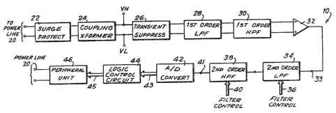
Figure 1 illustrates, in block form~ part of a circuit
for receiving a wideband data slgnal;
Figure 2 illustrates schematically an adaptive filtering
circuit wherein the filtering is controlled in response to varying
line conditions;
Figure 3 illustrates a code representation of a filter
control signal;
Figure 4 illustrates schematically a circuit for
7b 60285-845
transmitting a modulated, wideband carrier signal having digital
data encoded therein, the power of the signal being adaptively
controlled in response to changing impedance of the transmission
medium;
- 8 - ~ 3
t FIG. 5 illustrates schematically the transmit voltage
control block of FIG. 4;
FIG. 6 illustrates a voltage supply function provided
by the transmit voltage control circuit of FIG. 5;
F~G. 7 illustrates schematically a transmitter power
amplifier block of FIG. 4;
FIG. 8 illustrates a a data bit period according to the
invention, detailing the particular wave characteristics
used in a synchroni~ation scheme;
FIG. 9A illustrates a useful waveform for wideband
power line communication signals;
FIG. 9B illustrates a power spectrum for the waveform
of FIG. 9A; and
FIG. 10 is a state diagram depicting a method of
1 searching for and verifying reception of a data signal.
DETAILED DESCRIPTION OF THE PREFERRED EMBODIMENTS
FIG. 1 shows part of a power line communication (PLC)
circuit 10 for receiving data signals directly over a power
line 20 supplying AC power to a peripheral unit 46, such as
a remote printer, personal computer, or the like. Separate
data wires are eliminated by the inventive circuit. The
circuit 10 may be selectively coupled to the line ("hot")
and neutral conductors, or to the ground and neutral
conductors (not shown). In one embodiment, the AC line
conductor pair to be connected to is automatically selected
depending upon which of the two available pairs possesses
better signal transmission characteristics at any given
moment, i.e., less distortion, and better signal-to-noise
ratio for the data-carrying signal.
A line surge protector 22, such as a gas tube surge
absorber, may be applied across the signal line. The
selected conductors, in this example hot and neutral, may be
connected to the primary winding of a coupling transformer
24, the transformer removing the 60 Hertz AC voltage
provided by the AC power line 20. Line signals V~ and VL
- 9~ 33
1 are taken from the secondary winding terminals of coupling
transformer 24, the importance of these signals to be
explained below in connection with feedback control of the
in~entive transmitter section.
Transient voltage suppressors 26 may be applied between
each terminal of the transformer secondary and ground.
First order low pass filtering 28 and first order high pass
filtering 30 is applied to the received signals, using
well-known filters. According to the invention, the
modulated carrier used to convey data is a wideband phase
shift-keyed ~PSK) signal, having substantial energy across
the entire usable frequency range, i.e., between approxi-
snately lO0 kiloHertz (kHz) to 500 kHz. Below lO0 kHz, high
power noise spikes may provide interference to such an
extent that any reliable transmission may be difficult.
Transmission at frequencies over 500 kHz may radiate energy
into the broadcast AM frequency band, in violation of
applicable FCC regulations. Accordingly, the low and high
pass filters 28,30 substantially confine the signal frequen-
cy to the desired bandwidth. It will be understood that in
signal environments other than AC power lines, the defined
usable frequency spectrum may differ, and in that case, the
wideband data signal will contain energy over that particu-
lar bandwidth.
The filtered signals are applied to the inputs of a
difference amplifier 32, for example, including a JFET input
op amp, to provide the modulated carrier signal 33, less the
common mode noise. This signal 33 will be highly distorted
and will contain substantial noise components, despite the
signal conditioning already applied. Second order low and
high pass filters 34,38 may thus be used for equalization
and additional filtering of the modulated carrier signal 33,
enabling further signal processing, including reliable
demodulation. In a highly advantageous manner, selectively
controllable equal-component value, second order, Sallen-Key
filters are used. Digital switching control 36 is provided
~8~
1 to adaptively adjust both the cutoff frequency and damping
of the low pass section 34. Similarly, digital control 40
is applied ~o the high pass section 38 to adjust its cutoff
frequency and dampinq, as will be explained in greater
detail below.
After adaptive equalization, the signal is converted
from an analog, modulated carrier to a digital pulse signal
43 by any suitable means 42. In one simple and inexpensive
embodimen~, the conversion is accomplished by two-stage
clipped amplification of the carrier signal 41, the output
of the second amplifier then being applied to one input of a
high speed comparator in a circuit using hysteresis. The
digital pulse signal 43 is provided at the output of the
comparator. In another embodiment, an A/D converter having
longer bit length may be used to enhance processing gain, as
is well known.
The digital pulses 43 are applied to a logic control
circuit 44 for synchroni~ation detection and demodulation
(decoding) in order to recover the data embedded in the
pulse train, as will be explained further in connection with
various aspects of the logic processing circuitry. Once the
information is in the form of decoded data 45, it can be
passed along by the inventive PLC device to the peripheral
unit 46 coupled to the AC power line 20, thus accomplishing
the intended purpose of using the power line 20 for both
power supply and data communication.
Referring briefly to FIG. 2, detail of the advantageous
adaptively controlled, equal-component-value, Sallen-Key
filter sections is shown. While selection criteria of the
various circuit elements are well known, it can be seen that
the arrangement of FIG. 2 permits rapid adjustment of the
cutoff frequencies and damping effects of the filter
sections. Looking first at the low pass section, resistors
R2 and R5, and R3 and R6, may be selectively applied to
alter the cutoff frequency of the filter by switches, 54 and
52, respectively, which may be CMOS analog switches. The
4a3
1 six resistors Rl-R6 may thus provide four different frequen-
cies, depending on the switch positions. Capacitors C1 and
C2 are arranged as is customary. The feedback gain of the
amplifier 50, which may include a JFET input op amp, is
controlled by resistors R7-R10~ Selectively coupling one or
both of R8 and R9 with switches 56 and 58, respectively,
controls the low pass damping. The op amp output 37 is then
applied through capacitors C3 and C4 to the non-inverting
input of the high pass section op amp 60. Resistors Rll-R16
1~ may be applied to the non-inverting input signal in any of
four combinations to provide various high pass cutoff
frequencies, depending upon selective closure of switches 66
and 68. Damping is controlled by changing the feedback gain
provided by resistors R17-R20, through switches 62 and 64,
in a manner similar to the low pass section. This explana-
tion is intended as illustrative only, there being many
different methods of equalizing and filtering severely
distorted signals. Also, more switchable resistors could be
added, increasing the number of possible filter setting
combinations.
Adaptive control of the filter characteristics in order
to seek and maintain a highly equalized ratio may be
arranged by logic control circuitry 44, as follows.
Referring now to FIG. 3, a coded control signal for
switching the various resistors of FIG. 2 is shown, this
format being understood to be illustrative only. In a
control data byte 70 comprising eight bits 72, each bit 72
corresponds to one of the CMOS analog switches (52,54,56,S2,
6~,66,68) of FIG. 2. If a bit has value of logic '0", then
the corresponding analog switch may be closed; if the bit
is logical "1", the corresponding switch is open. Thus,
when the PLC device is not eeceiving properly ~iltered data,
as indicated by a high bit error rate, failure to achieve
synchronization, or some other specified condition, the
filter characteristics may be altered by issuing a new
filter "instruction" or setting, in the form of a different
- l2 ~ 3~3
1 sequence of logic "l"s and "O"s (another byte). In one
arrangement, each one of the 256 possible instructions is
tried for a predetermined period of time, on the order of 5
to lO milliseconds, until satisfactory data reception is
achieved, as evidenced by synchronization locking, low raw
bit error rate, or other performance criteria.
Leaviny the logic and microprocessor circuitry aside
for the present, and turning now to the transmitter section
of the invention, refenence is made to FIG. 4, partially
schematically depicting the transmitter section. In
general, a transmitter is arranged to create a desired
waveform from digital pulse trains provided by the logic
processing circuitry. The transmitter has the advantageous
feature of being able to satisfactorily transmit a waveform
having power spread across a very wide frequency spectrum,
e.g., lO0 kHz to 500 kHz, without substantially attenuating
the signal in any narrow intermediate bandwidth. In
addition, the transmitter is specially adapted to impress an
appropriate voltage onto the transmission medium, regardless
of the prevailing impedance of the medium, even as the
impedance varies.
Looking at FIG. 4, a peripheral unit 46, such as a
personal computer, may provide data signals 80 to be
transmitted to the logic control circuit 44 for encoding.
In the present illustrative embodiment of the invention, the
logic control circuit 4~ supplies two digital pulse trains
82,84 roughly corresponding to the positive and negative
portions of the ultimately transmitted waveform. The
voltage waveform is applied to a terminal of the coupling
transformer 24 secondary winding, as seen in FIG. l, for
transmission over the power line 20.
The digital pulse trains 82,84 may be applied to
control the operation of tri-state buffers 86,88 in a scheme
for creating the desired waveform which can have positive,
negative or zero val~e at different points in the time
domain. The tri-state buffers 86,88 are arranged to operate
- 13 ~ 3~3
in two modes, a high impedance block and a very low
impedance pass-through to ground. For example, when the
digital signal 82 has a positive pulse value +V, buffer 86
acts as a high impedance block, thus placing a voltage
si~nal on conductor 91 which is related to the controlled
voltage level on conductor 89, through resistor R30. The
significance of conductor 89 will be further explained
below~ Similarly, a voltage signal may be placed on
conductor 93 ~rom conductor 89 across resistor R31 when
digital pulse signal 84 holds buffer 88 in its high
impedance state. When the digital pulse signals ~2,84 have
values of zero, the respective buffers 86,88 resemble very
low impedance pass-throughs, causing the voltages on
conductors 91 and 93 to fall to zero. It can thus be seen
1 that since conductors 91 and 93 are applied to a difference
amplifier, which may include a JFET input op amp as is
known, a waveform is created on conductor 95 which may vary
between some positive and negative voltage level, such as a
sinusoid centered about zero voltage.
The generated waveform according to the invention has
power in a wide bandwidth covering substantially the entire
usable spectrum. Thus, it is necessary to generate this
desired waveform for each single carrier time period. An
information bit interval may actually be one or more carrier
periods in length, depending on the complexity of the
synchronization circuitry employed. A smaller number of
carrier periods per bit interval provides wider signal
bandwidth, the widest possible bandwidth resulting when one
carrier period is used for each bit interval. Synchroniza-
tion complexity is substantially reduced, however, where two
carrier periods per bit are used, rather than the optimum
one.
One time period of the carrier can be mapped into its
frequency spectrum usin~ known Fourier analysis techniques.
In order to practically synthesize the waveform, however,
the carrier period may be divided into a number of discrete
- - 14 -
1 sub-intervals (e.g., sixteen) each of which can assume n
discrete values, such as three voltages. Furthermore, an
anti-symmetric waveform my exhibit better transmission
characteristics than symmetric waveforms.
If sixteen sub-intervals are used for an anti-symmetric
waveform, and a pattern having three levels is ~esired, the
power spectrum will be a function of an eight-component
vector with each component being chosen from a set of three
values. This yields a finite number of possible waveforms
1~ having different power spectra, which may be searched. From
this group, a waveform may be chosen according to various
particular criteria, including relevant FCC regulations,
power distribution across the intended bandwidth, and
available circuit performance. One particular waveform
1 which has been found satisfactory is depicted in FIG 9A,
with FIG. 9~ illustrating its associated power spectrum.
Referring briefly to FIG. 9A, a useful waveform 200 is
shown~ the waveform comprising an anti-symmetric pattern of
sixteen pulses. The waveform 200 is but one of the possible
2n waveforms discussed above. Each pulse has a value of (+),
(-), or zero (202,206,204). In a particular embodiment of
the invention, each pulse interval is approximately 250
nanoseconds in length. The waveorm is generated by
controlling the tri-state buffers 86,88 as described above.
FIG. 9B shows a power spectrum 210 of the waveform 200
of IFG. 9A. The waveform 200 has been mapped into a power
versus frequency spectrum using Fourier analysis, as is
generally known. As illustrated, substantial power is
approximately uniformly spread across a useful frequency
bandwith, i.e., above 100 kiloHertz and below the AM
frequency band. The power spectrum remains below the
external FCC design limitation for digital power transmitted
in the regulated AM portion of the spectrum. The waveform
is intended to ber and will be understood as illustrative
only, and other waveforms may also satisfy the desired
design criteria.
- 15 -
.f~
Before power amplification, the signal must be filtered
in order to ensure that power is not radiated outside the
intended frequency bandwidth. Such extraneous transmissions
re~uire power better spent elsewhere, and may run afoul Gf
FCC limitations on radiated transmission frequencies.
Accordingly, the waveform on conductor 95 is applied to
first order low and high pass filters 92, with subsequent
gain control 94 being applied. The particular techniques
used may be customaryO Second order low pass filtering 96
1~ may also be employed, such as a unity-gain, Sallen-Key,
second order low pass filter.
Finally, power amplification 98 is provided, which may
be a voltage controlled voltage source (VCVS) in the general
form of a feedback amplifier, having the advantageous
characteristics of reduced noise, low frequency distortion
and low phase distortion. In one particular embodiment of
transmitter power amplifier section as shown in FIG. 7, the
output of an op amp 130 is used to apply a signal to the
bases of common emitter-arranged Darlington transistors
132,134. Amplifier feedback control is provided through
resistor R51 in parallel with capacitor C10, through series
resistor R50, and applied to the inverting inp~t of the op
amp 130, which once again may be a JFET device. The op amp
output may be applied through resistor R52 to a point along
a number, in this case five, of slow rectifier diodes D3-D6,
such as lN4001s. The slow diodes D3-D6 help eliminate
crossover distortion, and make possible the use of lower
biasing currents ~or the Darlington transistors 132,134.
The diode network is biased by resistors R53 and R54.
A collector-to-base voltage drop of transistor 132 is
provided by applying voltage -V3, which may be -15 volts,
directly to the collector. As shown, the collector is
coupled ~o ground via capacitor C12. Transistor 134 is
similarly powered by the voltage +V3 applied directly to the
collector, the collector also coupled to ground through
coupling capacitor C13.
- 16 -
83
1 The emitter voltages of transistors 132 and 134 are
applied, through resistors R55 and R56, respectively, to the
amplifier output VH, through resistor R58. Analog switches
(not shown) may be used to bypass op amp 130, and to isolate
the transistor bases from their supply voltages ~/- V3, when
the transmitter is not operating. In this situation, the
line vol~age appearing at VH is capacitively coupled to both
transistor bases via series-coupled resistors R57,R58 and
then through capacitors C14 and C15. This arrangement
advantageously causes the transistor base voltages to float
with VH, ensuring that the transistors 132,134 remain off
and quiet.
As mentioned earlier, the transmitter is arranged so as
to place a proper voltage level on the power line 20 despite
changing impedance of the line. This is now explained with
reference to the as yet unexplained portion of the illustra-
tive circuit shown in FIG. 4. The modulated waveform at V~
is applied to one terminal of the coupling transformer 24
secondary winding. VL is coupled to the other secondary
winding terminal, as shown in FIG. 1. VL is also connected
to capacitor C8 in parallel with resistor R33. The voltage
l01 at the low side of resistor R32 is applied to grounded
resistor R33. Thus, the voltage drop across R33, as
indicated at 101, is related to the voltage placed on the
power line by the transmitter at VH. Since a particular
voltage range can be considered optimum for the transmitted
signal, the detected voltage 101 is used to control the
original signal levels provided by tri state buffers 86 and
88.
One arrangement for accomplishing this feedback control
is suggested in FIG. 4. Voltage 101 may be applied to first
order high pass filter 10~ so as to eliminate unwanted
signal in the frequency band no~ of interest. Means 114 for
determining a control signal related to the average trans-
mitted power is provided. For the sake of simplicity, a
half-wave rectifier 104 may be used to cancel the negative
- 17 - ~ 3
1 signal portions which would act to cancel out the detected
power altogether, it being understood that the detected
signal will be related to one-half the total transmitted
power. The rectified signal is applied to a ~ime constant
circuit 106 having microcomputer control 108 ~or adjusting
the time response of the feedback loop, the response being
quick when transmission first begins, but then slowing down
as transmission is continued. This prevents amplifier
operation at improper levels for extended periods of time.
1~ ~n a~erage power level may then be provided by first order
low pass filtering 110, using known ~ilters. The detected
average power is applied to a transmitter voltage control
circuit 112, which provides the unamplified signal voltage
levels to conductors 91 and 93 through resistors R30 and
R31, respectively.
The transmitter voltage control circuit 112 may be any
arrangement which provides a certain voltage output as a
function of voltage input. One such function is shown, as
an illustrative example only, in FIG. 6, a curve 126 of
control circuit 112 output voltage VoUT as a function of
average transmitted power. For average power above a
certain level 132, the output voltage is held at a first
level Vmin. For detected average power less than another
certain level 130, the output voltage may be VmaX~ In a
range between the two levels 130 and 132, the output voltage
may monotonicallY decrease from VmaX to Vmin Such a
function is provided by the control circuit 112 shown in
FIG. 5. Negative feedback amplifiers, which may include
JFET input op amps 120,122 and resistors R40-R44 as is
customary, are series-coupled, the output of the first op
amp 120 applied to the inverting inputof the second op amp
122. At a point between the op amps 120,122, the voltage is
clipped by switching diodes Dl and D2, one diode Dl coupled
to ground, and the other being supplied a voltage Vl which
may, for the sake of convenience, be equal to a voltage
supplied to the inverting input of the first op amp 120
- 18 ~
1 through resistor R40. Voltage Vl may be, for example, 3.3
volts. The non-inverting input of the second op amp 122
receives an applied voltage V2, which is equal to Vmin, and
which may be, for example, 2.76 volts. VouT is thus
increased as the inverting input voltage of op amp 122 goes
further negative from zero.
In this manner, the transmitted power is feedback controlled
in response to changes in detected voltage 119.
According to another aspect of this control, the
10 component values for C8, R33, and R58 may be specially
chosen so as to permit pro~er transmitter operation in
series combination with the inductance of the peripheral
unit's line cord, even when the transmission medium imped-
ance is so low as to approximate a short circuit. The
impedance may, of course, e capacitive, resistive or
inductive, or any combination of the three. It is estimated
that the lowest impedance which might be enco~ntered would
result from a resistance on the order of 1-2 ohms, a
capacitance of approximately 0.2 microfarads (the line side
capacitance caused by a personal computer's FCC-required
filter), and roughly a 1-2 microhenry inductance.
The following is a list of component values for one
embodiment of the invention as described above (resistors in
ohms, capacitors in picofarads, except as noted):
25 Resistors Capacitors
Rl,R4 l.lOk Cl 720
R2,R3,R5,R6 5.76k C2 180
R7,R8,R9,R10 5.76k C3,C4 330
Rll,R13 2.43k C6 180
R12 3O74k C8 0.5 microfarad
R14,R16 9.76k C10 100
R15 l5.0k C12,C13 10 microfarad
R17,R18 9.76k C14,C15 10 nanofarad
Rl9,R20 9.76k
R30,R31 887
35 R32 10
-- 19 --
1 R33 2.7
R40 34.8k
R41 40.2k
R42 2k
R43 52.3k
R44 34.8k
R50 150
R52 620
R53,R54 15.0k
10 R55~R56 1.2
R57 ~k
R58 2.7
In order to properly receive and decode data communica-
tions, the receiver section must search for and lock into
synchronization with the carrier signal phase. Means are
provided for comparing a received signal with a predeter-
mined signal known to identify an information bit, as
opposed to noise. Generally, the received signal is
repetitively compared with the known reference until a
certain level of correlation is found to exist between the
two patterns. It sho~ld be noted that substantially similar
rates of transmission and reception among all transmitters
and receivers must be maintained in order to properly
examine the correlation. In one embodiment of the
invention, each circuit is provided with a crystal oscilla-
tor as a pulse timing reference. Since crystals having
accuracies on the order of 100 parts per million are readily
available, use of a crystal having a frequency of, for
example, 4.3008 megaHertzt completely eliminates the prior
need for tracking the data signal frequency.
A receiver may sit idle when neither receivinq nor
transmitting data. The receiver will monitor signals coming
over the power line, however, in the event that a data
transmission has been initiated. A special series of
information bits may be provided for allowing the receiver
to capture and verify the signal. In a phase shift-keyed
- 20 - ~ 3
1 carrier, logic "l" and logic "0" have equal, but inverted,
waveforms. Thus, the special series might be identified, in
part, by a sudden change in sign of a sufficiently high
correlation count.
The search/verification scheme is described in conjunc-
tion with ~IGs. lO and 8. Referring briefly to FIG. 8,
certain details of the searching scheme are explained. In
an embodiment of the invention, a data bit period 402 is
equal to two successive carrier periods 404, here represent-
ed as perfectly undistorted sine waves. It will be under-
stood that the actual waveform will be highly distorted and
in practice, the highest energy portion is clearly the
waveform segment indicated. If a carrier period 404 is
divided into sixteen intervals, it is seen that an
8-interval segment 408 can be created over the interval of
the wave having the highest energy content. This portion of
the signal may be roughly approximated by a step waveform
410 over the 8-interval segment, and it is this step segment
~lO which is used as the reference for correlation according
to the invention. The resulting count for the 8-interval
correlation may range from -8 to ~8, the latter representing
perfect correlation, the former representing a perfect but
inverted waveform.
Referring now to FIG. lO, a state diagram for a power
line sommunication synchronization scheme is shown. The
state diagram may be embodied in logic circuitry including a
classical finite state machine, using well known techniques.
When a signal appears on the transmission medium, the signal
is correlated with the known reference signal interval. In
this embodiment, a user data message is prefaced b~ a
3~ sequence of bits, e.g., seven "O"s followed by a "l",
followed by a signature byte which is as unrelated as
possible to either the sequence of seven "O"s followed by a
"l", or its opposite, seven "l"s followed by a IOn.
A correlation count is obtained in an initial "state"
301. If perfect correlation is found (C=+8), it is possible
1 that the beginning of a sequence of seven "onS has been
located, and the control moves to a next state 303 in order
to begin the process of verification. A new correlation
count is obtained at a point shifted in time from the
previous correlation count, in order to test the next
expected signal for presence o the reference interval. The
shift corresponds to skipping an 8~interval segment of the
waveform which would be expected to correlate with the
opposite sign. If perfect correlation had not been found (C
less than +8), another count would be made at state 301.
According to the invention, this process is monitored by a
microcomputer. If a number of correlation counts have been
made without success, the system adaptively changes the
receiver filtering by issuing a new instruction byte 70, as
explained in conjunction with FIGs. 3 and 4. This general
pattern continues as explained below.
In the second state 303, a sufficient correlation count
will elevate control to the next state 305. From this point
on, correlation sufficiency may signify a count greater than
or equal to +6. It should be apparent that this is merely
one particular embodiment of a synchronization scheme, many
others being possible. If the count at state 303 was
insuficient (C less than ~6, or wrong sign), then control
drops back to the first state 301. (The proper sign must be
determined at the beginning of the process.) This pattern
continues identically through the next two states 305,307
until state 309 is achieved. Achievement of state 309
signifies that successful correlation has occurred four
times, and at this point, there may be some confidence that
the sequence of "O"s followed by the "1" is actually being
received.
State 309 is maintained so long as successful correla-
tion counts are obtained. The system is now waiting for a
sufficiently high count having the opposite sign which
signifies the end of the predetermined pattern, at which
time state 311 is reached. During this waiting period, if
33
1 an insufficient count is obtained (C less than ~6), another
intermediate waiting state 315 is achieved. Upon the next
successive correlation count, control will either be
returned to the previous waiting state 309, or dropped to a
lower confidence level waiting state 317 (since two bad
counts have thus occurred consecutively, indicating that the
bit sequence may, in fact, have been no more than noise).
From either of states 317 or 315, a good correlation will
raise the confidence level back toward waiting state 309.
An insufficient count tC less than ~6) while at state 317
will cause operation to restart at the beginning state 301
(three successive bad counts obtained strongly indicates
reception of noise).
From any of states 309, 315 and 317, a sufficiently
high correlation count having an opposite sign causes
elevation to one of states 311 and 313. If the next
succeeding correlation count while in either of these states
is insufficient (C less than +4), operation is dropped back
to level 305 or 303, respectively, in an attempt to pick up
the special bit sequence again. If the count is sufficient
when in state 311 or 313 (a repeat of C greater than or
equal to ~, opposite sign), a very high confidence state 321
is reachedO At this point, a final correlation count is
taken over the next 16 immediately succeeding intervals,
i.e., one full carrier period. IE a 4-bit counter is being
used, it is apparent that the value cannot go any higher
than +8, nor any lower than -8. For such an implementation,
all correlation counts which are better than -8 (covering
three-quarters of the possiblilities, since an actual -10
will only read as -8 due to the bit limitation of the
up/down counter) will cause the logic control to begin
dumping the data to the microcomputer. In the very rare
instance that the count is -8 (signifying anything ~rom -8
to -16), the entire process is aborted and then restarted
from state 301.
- 23 -
1 It should be noted that the receiver synchronization
may be shifted in time, even substantially, from the actual
start time of a transmitted bit interval. This is made
possible by correctly selecting both the transmitted
S waveform and the demodulation reference waveform. This
contributes to the important benefit that the P1C system
according to the invention will successfully synchronize in
the presence of a wide variety of line characteristics.
Once it has been assured that data bits are being
received, network access control may be transferred to a
microcomputer, as mentioned previously. Special data link
protocols for use in local area networks (LANs) are known,
but these protocols are nott in general, sufficiently robust
so that data may be accurately communicated over a medium
which is highly error-prone. For example, data may be
transmitted in packets, each packet containing a large
number of bytes. Error checking, such as CRC, may be added
to the end of the packet. When transmitting over power
lines, however, the probability of error is so high that the
value of such known error checking methods is reduced.
Thus, packets are advantageously broken apart and recon-
~igured into smaller frames, since the probability of
receiving an erroneous frame is much lower than that of
receiving an erroneous byte somewhere in a packet.
Another advantage of using smaller size frames is that
it becomes possible to employ various error correction
techniques in combination with error detection techniques to
provide an extremely reliable data link. In particular, it
is desirable to provide correction for all single bit errors
in a transmitted byte, and also all two-bit burst errors.
An error correction code/error detection code ~ay be
provided which substantially accomplishes this goal.
As an example, assume transmission of a byte haYing
eight bits is desired. To perform error correction, an 8/4
code might be provided which encodes one-half the byte at a
time, mapping the four bits into one of sixteen possible
- 24 -
~8~3~
1 8-bit codewords. The codeword is transmitted, and then
decoded by looking it up in a decoding table 256 bytes long
(28 possibilities). Any codeword which contains errors will
be assumed ~o have originated as one of the 16 "real"
codewords, i.e., some correspondence may be predetermined
between the 16 real codewords and the 240 spurious code-
words.
Very serious errors, i.e., so bad that the scrambled
codeword byte might even resemble another "real" codeword
when received and decoded, may be handled by the addition of
error detecting code. The original data byte is mapped to a
corresponding edc byte of 8 bits. This edc byte is then
split up, each four bits are mapped into codeword bytes
using the error correction table and transmitted as well.
1 Thus, it should be apparent that the particular embodiment
being described is relatively inefficient, each data byte
re~uiring four transmitted error correct-coded bytes: for
the first four bits of the data byte; for the last four
bits of the data byte; for the first four bits of the edc
byte; for the last four bits of the edc byte. When the edc
byte is reconstructed, it is mapped back to something which,
if all has gone well, is the original data byte. If not, a
serious error has been made and retransmission may be
requested. These are only some of the many features which a
PLC system should handle in implementation of a data link
protocol.
As thus described, a novel power line communication
system is provided, having vastl~ improved reliabilty and
higher data transmission rate than previously ~nown PLC
systems. As will be plain to those skilled in the art, a
great number of variations, modifications and additions may
be made to the disclosed detailed embodiment, which is
illustrative only, without departing from the spirit or
scope of the invention. For example, as digital technology
continues to progress, it will become economical to perform
much of the filtering and equalizing with purely digital
- 25 ~ 3~3
1 devices, instead of the familiar resistance-capacitance
networks as described. Waveshaping may also be economically
accomplished with digital devices at some point.
At the present time, however, the invention in a form
S as disclosed can be manufactured and sold at a very low
cost, less expensive than other known systems by as much as
an order of magnitude or more in price difference. It is
especially adapted for use in local area network (LAN)
configurations, providing an internal protocol which
1n provides fast, reliable network access and control over the
transmission medium, whether in a master/slave, distributed
master, or token bus/token passing mode of communication and
control.
The invention is limited only by the appended claims.