Note: Descriptions are shown in the official language in which they were submitted.
1~80523
271 9US
SIGNA~ COMPENSATION CIRCUITS
~ACKGROUND 0~ THE INVENTION
1. Field of the Invention
The present invention relates to signal
compensation circuits for example ~or compensatin~
the output signals from detection devices and in
particular ~or compensating the outPut from door
detection devices in li~t or elevator doors.
?. Description of the Prior Art
In a previously proposed system in its
simplest form a pair o~ sensors are mounted in spaced
apart relationship along the leading edge of a
sliding door. ~he output of the sensors is monitored
and when a difference in levels of the two outputs is
detected, this indicates an irregular shaped
obstruction (for example the human form) in the
doorwa,y. The system is intended to operate on the
principle that the sensors which are mounted on the
leading edge o~ the door, monitor the door space as
the door closes. When the sensors sense the presence
o~ the slam post as the door closes the sensors
respond equall,y and so that there is no difference in
the level o~ the two output signals produced. When
the human ~orm moves into the door space the shape is
irregular and so the two sensors respond differently
producing output signals having different levels. A
control circuit can be used to respond to this
di~erence to retract the door as a safety measure.
With such systems the operation is never
ideal and the two sensors ma,y produce different
output levels even when no human ~orm intervenes into
the doorway. For example, the slam post may not be
parallel to the sensors and dust may gather on one of
the sensors and not the other. One sensors may have
components which prematurely age.
, .. .
~ 2805Z:~
2719U~
In order to avoid responding to such
differences, it has been proposed to compare the
difference between the two outputs at di~ferent times
during the closure of the door in order to
distinguish between variations produced b~ static
components such as a non-parallel door post and
variations produced by moving objects such as the
human form. An appropriate control signal is then
produced by comparing an actual difference signal
with a delayed difference signal.
SUMMARY OF ~HE I~V~IO~
.
According to the present invention there is
provided an error compensation s~stem comprising an
input and an output terminal interconnected b~ a
signal modi~ing circuit having a control input,
comparison means connected to the output terminal to
compare the signal at the output terminal with a
reference signal to produce an error signal, first
and second delay circuits having substantially
dif~erent time constants and each connectable to
Aelay and feed the error signal to the control input
of the signal modifying circuit, and switch means
operable in response to a predetermined condition to
cause a selected one of the delay circuits to feed
the error signal to said control input.
According to the present invention there is
~urther provided an error compensation system
comprising first and second terminals, a comparator
having two inputs respectively connected to the first
and second terminals and having an output, an
integrator comprising resistance means and
capacitance means connected to the output of the
comparator, control means responsive to a
predetermined condition to alter the value of at
least one of said resistance and capacitance means to
~Z805Z3 271 ~us
change the time constant of the integrating means,
and modif~ing means ~or receiving an input signal and
supplying it to the first terminal, the modifying
means being responsive to the output of the
integrator to modify the input signal in a sense to
maintain the signal at the first terminal
substantially constant.
According to the present invention there is
yet further provided a signal compensation s~stem
comprising ~irst and second sensors each providing an
output in response to a monitored condition, means
responsive to the output of the first sensor to
provide a quasi reference signal, a comparator for
comparing the output of the second sensor with the
quasi reference signal to produce an error signal,
feedback means responsive to the error signal to
modi~y the output of the second sensor in a sense to
equalise t with the quasi reference signal, a first
time delay circuit having a first time constant
connected to delay the error signal in the feedback
circuit, a second delay circuit having a second time
constant less than that of the first time constant
actuable to delay the error signal in the feedback
circuit to a lesser extent, and trigger means
responsive to a predetermined condition, to actuate
said second dela~ circuit.
~RIEF DESCRIPTION OF THE DRAWI~GS
An error correction system embodying the
invention will now be described by way of example
with reference to the accompan~ing diagrammatic
drawin~s in which:
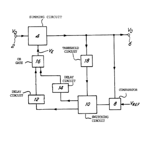
Figure 1 is a block diagram oY the system;
and
Figure 2 is a circuit diagram of the system
applied to a lift door detection circuit.
i~80S23 2719US
DESCRIP~IO~ 0~ ~HE PRE~ERR~D EM~ODIMENTS
~ he error signal correction system ~hown in
~igure 1 includes an input terminal 2 for receiving
the output si~nal VD of a sensor (not shown)
monitoring a predetermined condition. The circuit to
be described is arranged to ad;ust the level of the
sensor signal VD to a level determined by a
reference signal VR~F so that the error signal is
continuously corrected ~or variations.
~he correction sy~tem includes a summing
circuit 4 for receiving the signal VD from the
input terminal 2 and a correction signal VE from a
~eedback loop which adjusts the value of the signal
VD accordingly before directing it to an output
terminal 6 as a signal VO.
A comparator 8 compares the signal VO at
the output terminal 6 with a re~erence si~nal VRE~
(which may be either a fixed or variable signal) and
produces an error signal which is ~ed to a switching
circuit 10. The switchin~ circuit 10 is switchable
to direct the error si~nal to one or other of two
delay circuits 12 and 14 having substantially
di~erent time constants, and the outputs of the
delay circuits 12 and 14 are fed via an OR ~ate 16 to
a control input of the summine circuit 4.
A threshold circuit 18 monitors the voltage
VO and when a predetermined threshold is exceeded
~or a predetermined period o~ time it will cause the
switchine circuit 10 to switch from feeding the delay
~0 circuit 12 with the longer time constant to the delay
circuit 14 with the shorter time constant. Equally
when VO again drops below the threshold level it
will switch back again.
In operation relatively slow variations in
~5 the sensor output signal VD are detected b~ the
~2805~3
2719US
-- 5
comparator 8 and an error ~ignal is produced which is
fed through the delay circuit l2 (with the longer
time constant) to correct the signal VD in the
summing circuit. Thus, for slow variations in VD
even though they are progressive, the output signal
V0 will remain substantially unchanged.
When a fast variation in the signal VD
occurs, the dela~ provided b~ the dela,y circuit 12
will not allow the change in error signal ~JE to
reach the summing circuit 4 in time and the output
signal V0 will change. When this change exceeds a
threshold level and lasts for the predetermined
period of time as determined by the threshold
circuit l8, the switching circuit will switch the
output of the comparator 8 to the shorter t me
constant delay circuit l4, thus effectlvely speeding
up the effect of the error correction signal. As
~oon as the detection signal VD falls below the
threshold level of the threshold circuit 18 the
switchin~ circuit 10 will redirect the error signal
via the dela~ circuit 12 having the longer time
const,ant.
With this arrangement it will be
appreciated that the detection sienal is normall~
desensitised against errors due to drift and other
slow varying influences and that when a fast varying
change occurs which subsists for a predetermined
period of time the system will attempt to draw the
sienal VD back to its previous level at a much
faster pace tif VREF remains unchanged) and as soon
as this i8 achieved the slow rate of error correction
action i8 again brought into play.
It will be appreciated that while the
switching circuit 10 switches in response to the
~5 threshold circuit 18, it can be made to switch in
~280~23
2719US
response to some other predetermined condition
instead.
~igure 2 ~hows an embodiment incorporating
the principles of ~igure 1. As shown, four sensors
20, 22, 24 and 26 are mounted in vertically spaced
relationship along the leading ed~e of the sliding
door (not shown~ of a lift or elevator. ~ach sensor
monitors the space locally between the leading edge
of the door and the slam post (not shown) against
which the door will eventuall~ close.
A number of arrangements of such sensors
are disc,Iosed in our co-pending Canadian patent
application 522,201.
The four sensors 20 to 26 are coupled to
respective input terminals 100 to 103. The four
input terminals 100 to 103 are coupled to respective
ones of four output terminals 133 to 136 via a
corresponding one of four summing circuits 106 to
109,
An input terminal 105 is provided to
recçive a reference signal VREF and an input
terminal 104 is provided to receive a trigger signal
V~ .
The summing circuit 109 has one input
connected to the input terminal 103 and its other
input connected to the reference voltage input
terminal 105. In this way the output of the summing
circuit 109 will generall~ alwa~s be offset from the
reference voltage VR~F.
Each of the three summing circuits 106, 107
and 108 has an associated feedback loop. Only the
feedback loop associated with the summing circuit 108
will now be described, but it will be appreciated
that in the other two feedback loops, similar
components will be given similar references (but with
l~aoSZ3 27~0us
the suffix A and B respectivel~) and that their
function and operation ~re similar to that of the
feedback loop associated with the summin~ circuit
108.
As shown, the feedback loop comprises a --
comparator 113 connected to compare the outputs from
the two summing circuits 108 and 109. The output of
the comparator 13 feeds allRC time dela~ circuit in
the form of an integrator comprising a first
resistor 122 and a capacitor 126 connected in series.
A second resistor 123 having a substantiall~ lower
value than the first resistor is connectable in
parallel with the first resistor through a switch
117. The junction between the resistor 122 and
capacitor 126 is coupled via a line 139 to the second
input of the summing circuit 10~.
A pair of zener diodes 131 and 132 are
connected in series opposition between the reference
terminal 105 and the line 13a to clamp the signal on
line 139 to a predetermined level when the si~nal on
line 139 reaches a level wh,ch exceeds the reference
voltage level b~ a predetermined amount.
The four output terminals 1~3 to 136 are
coupled to a comparison circuit 150 which will
respond to one of the outputs being signif~cantl~
different to the others to ~enerate a trigger si~nal
VT which is then fed to input terminal 104.
The comparison circuit 150 ma~
advantageousl~ take the form shown in our co-pending
3 Canadian patent application 522,201.
The output of the input terminal 104 is fed
via an as~metrical dela~ circuit 110 to control the
operation of the switch 117.
In operation under stead~ state conditions
each feedback loop will correct the output signals
~2805~3
2719US
-- 8
from respective ones of the output terminals 133 to
135 to equalise them with the level of the output
signal Irom output terminal 136. Thus the outputs
from all four output terminals will all be at the
5 same level.
Thus, whatever the individual setting of
the individual sensor, their outputs from the four
output terminals will, aîter a settling period
following energisation, all be the same.
Thus, even if dust settles on the surfaces
of individual sensor or if selected components age
prematurel.y, or if they react differently to changes
in ambient conditions, they will ~till all be brought
to equal levels. Also if each sensor produces a
significant change in output signal, then provided
the differences between all four sensor outputs
varies relatively slowly the signals at all four
outputs will remain equal.
If now one sensors (for example 24)
produces a rapid change in output which is different
to that produced by the other sensors (20, 22 and 26)
then initially the output signal from output terminal
135 will be significantly different from the output
at the other terminals. This difference will be
detected by the comparison circuit 150 which will
generate a trigger signal VT which if ~ustained for
a suff`icient period (typically 10 seconds) as
determined by the delay circuit 110 will cause the
switches 117, 117A and 11713 to close.
This action will now allows the feedback
loop to rapidly equalise the output signal at
terminal 135 with the output signals at the other
terminals 133, 134 and 136. For example, if the
delay provided by the RC delay circuit chan~es
typloQll~ fro= 15.0 to 0.25 s~conds, the fee~bac~:
.
.
~.~80~ 3
2719US
g
circuit is effectivel~ short circuited until
equalisation has again been achieved. If after the
10 seconds delay provided by the circuit 110 the four
signals at the four output terminals 133 to 136 are
brought back to equalit.y by the feedback loops, the
comparator 150 will no longer detect inequalit,y and
the trigger voltage will disappear. ~he switches
117, 117A, 117B will accordingly open and normal
operation will resume.
If the output of one of the sensor exceeds
the reference voltage by a predetermined amount, for
example b~ a hand being placed directly over one of
the sensor with a view to holding the lift door open,
then the clamping circuit defined by the two zener
diodes 131 and 132 comes into operation and ~urther
adjustment of the sensor signal b~ the feedback loop
will be inhibited until the output signal from the
sensor resumes a more normal level.
It will of course be appreciated that the
error correction system described acts to
automatically balance the outputs of the four sen~ors
at all times. The rate of balancing is normally
relatively slow but when a signal representative of a
selected condition to be detected is sensed and
sustained for a predetermined period of ~ime, then
the system will switch to a mode of operation in
which the rate of balancing i9 relatively ~ast. As
soon as the balance is achieved the system reverts to
its relatively slow balancing mode.
~0 It will of course be appreciated that the
triBger signal VT is also used to trig~er the
opening or re-opening of the lift door since there
will only be an imbalance of signals on terminals 133
to 136 when an irregular object such as the human
form is detected in the door opening.
~80~i~23
2719US
_ 1 0
It will also be appreciated that the
circuitry can be equally adapted to respond to
d,gital or analog signs. In the digital ~orm, the
signals from the four sensors are multiplexed and
said the comparators operate in an on/off mode.
In a modification, instead of the switch
117 being used to var,y the resistance of the
resistive part of the integrator defined by the
resistors 122 and 12~ and the capacitor 126 it can be
used to modify the capacitance or both to achieve the
necessary change in time constant.
Of course, while the error correction
s,ystem has been described in conjunction with a lift
door detection system, it has apnlication in many
other fields such as robotics as will be apparent to
the person skilled in the art.
While a presently preferred embodiment of
the present invention has been illustrated and
described, modifications and variations thereof will
be apparent to those skilled in the art given the
teachings herein, and it is intended that all such
modifications and variations be encompassed within
the scope of the appended claims.