Note: Descriptions are shown in the official language in which they were submitted.
)'95
1 51,930
.: MULTIPURPOSE DIGITAL INTREGRATED CIRCUIT FOR
COMMUNICATION AND CONTROL NETWORK
5~8~L~L~ TO RELATED APPLICATIONS
The invention disclosed herein relates to two-
way communica-tion and control sys~ems. Canadian patent
application number 484,817 filed June 21, 19~5, entitled
.~ "Digital Message Format for Two-Way Communication and
Control Network", invankors Leonard C. Vercel'lotti,
:~ ~ William R. Verbanets Jr. and Theodore H~ York, relates
1Q to such communication and control systsms.
'
BACKGROUND OF THE INYENTION
' ~ A~ Field of the Invention
~-' The present invention relates generally to
~' information communication networks and, more
particularly, to communication networks by means of which
'; a large number of remotely positioned controllable
, devices, such as circuit breakers, motor overload relays,
; lighting systems, and the like, may be controlled from a
~ central or master controller over a common network line
.
~;
.~
:,
:,
. ' : , '
.. ,: . .` ~ . ' .` ' ~ '
:
`
~81~
2 51,930
which may comprise eith~r the existing AG power lines, or
a dedicated twisted pair line, or in some instances a
fiber optic cable.
The invention particularly relates to a low
Gost, multipurpose digital integrated circuit (IC) which
can be used as the basic ~uilding block in establishing
a network communication system over a desired
communication link. The digital IC can function as an
addressable microcomputer interface between the network
line and a remotely located microcomputer which may, for
example, comprise any microprocessor based controlled
product. In such mode, the digital IC5s function is to
take data from the network and pass it on to the remotely
located microcomputer upon command from the central
controller and to transmit data from the microcomputer to
the central controller. The digital IC may also function
a~ a nonaddressable microcomp~ter interface between the
central or master controller and the network line. In
such case the digital IC's function is to continuously
take data from tho central controller and place it on the
~ network and take data from the network and pass it back`~ to the central controller. The digital IC may also
function as an addressable load controller associated
with an individual remote controlled device and
2~ responding to shed or restore load commands from the
central controller over the network line. When so used
; the di~ital IC may also be commanded to transmit a reply
message back to the central controller giYing information
as to the status of the controlled device, thus enabling
the central controller to monitor a large numbler o~
remotely located controllable devices.
B. DescriPt1on of the Prior Art
Various communication and control systems have
~` been heretofore proposed for controlling a group
~,'
~ .
, , , , - :
.,
L0~3~
3 51930
of remotely located devices from a central controller over
a common network line. Control systems for controlling
distributed electrical loads are shown, for example, in
Miller et al V.S. Patent Nos. 4,167,78~, 4,367,414 and
4,396,844 issued SeptembPr 11, 1979, January 4, 1983 and
August 2, 1983~ respectively. In such systems a large number
of relatively complex and expensive transceiver-decoder
stations, each of which includes a microprocessor, are inter~
connected with a central controller over a common party line
consisting of a dedicated twisted pair for bidirectional
communication between the central controller and all trans-
ceivers. Each of the transceiver-decoder stations is also
of relatively large physical size due to the fac~ that a
substantial amount of hardware is required, in addition to
the microprocessor, to receive and transmit signals. Also,
both the hardware and microprocessor consume substantial
amounts of power. In fact, in Miller et al U.S. Patent No.
4,167,786 it is necessary to provide a powersa~er mode in
which the major portion of the circuitry at each remote station
is denergized to reduce power consumption during intervals
when load changes are not being actuated.
Each of the transceiver-decoder stations controls
a number of loads which must be individually connected to a
particular transceiver by hardwiring, these interconnections
being quite lengthy in many instances. In such a system, all
transceivers can initiate messages at any arbitrary time in
~ respon~e to control input from the associated switches. Ac-
~ cordingly, it is not uncommon for two or more transceivers
- to simultaneously sense a free common party line and begin
simultaneous transmission. This requires a special bus
arbitration scheme to cause all but one of the interfering
- transceivers to drop out of operation while permitting
one seleFted trans-
.
::
. : , - , , .
- ~ . ...
,
,
:
.
4 ~8~95 51~3~
ceive~ to continue its data transmission. Also, in
such a.systam tran~mission from the transceiver to
the central controller is very limited and consists
merely o an indication of a manually opera~le or
condition responsive switch or analog sensor~ such as
a thermistor or other analog sensing device. In ~he
load distri~ution control system shown in ~he a~ove
referenced prior art patents, the arbitr~tion ~ech-
nique is dependent on the impedance levels of the
active and inactive states of t~e data line. If the
data line DeCOmeS StUC~ in a low impedance state, due
to the failure of one of ~he connected ~ran~ceiver
decoders, further communication over the network line
is prevented until the malfunctioning transceiver is
pnysically disconnec~ed ~rom the data line.
In the communication aRd control sy~tem de-
scri~ed in the a~ove identified Miller et al patents
a message transmitted over the networ~ includes a
pream~le portion of a minimum of four bits. Tnese
preamble bits comprise sa~ square waves which are
u~ilized by the ~ransceiver decoders to permit a
phase loc~ loop circuit in each ~ransceiver to lock
onto the received preamble ~its. The use of a mini-
mum o~ four bits to provide phase loop lockon reduce5
~ 25 ~ the overall throughput of such a system. Also,
: in order to capture ~he preamble bits it is necessary
to provide the phase loc~ loop circuit initially with
a relatively wide ~andwidth of a~out 5KHz and then
narrow down the ~andwidth after the phase loc~ loop
circuit has locked onto the pream~le ~its. Such an
arrangement requires additional circuitry to accom-
plish the necessary change in bandwidth. Also, the
relatively wide ~andwidth necessary to capture the
: preamble bits also lets in more noise so that the
security and reliability o~ the system is reduced in
noisy environments.
;
., .
8~
5 51~30
In the presently described communication
network a small low cost digital IC is employea which
can be readily adapted by merely grounding different
S input terminals oF the IC to perform all of the dif-
ferent functions nece3sary to the ccmponent parts of
the complete communications net~ork. ThuS, in one
pin configuration of the digital IC it can function
as an addressable load controller, responding to shed
or restore load commands from tbe central controller
and replying back to the central controller wi~h
stat~s inormation regarding the st~te of the con-
trolled load. This mode of functioning of the digi
tal IC is ref erred to as a stand alone slave mode of
operation. In the stand alone slave mode the diqital
IC is arranged to De directly associated with ,each
~ control device i.e. circuit ~reaker, motor control-
`: ler, lighting control, etc. and may, if desired, com-
~-~ munica~e with the master con~roller over the same
~: 20 wires which are used to supply power to the control-
led device. This substantially reduces the amount of
wiring required to connect a number of controlled de-
-~ vices to the common communication network. The cen-
~: tral ~controller m~y also:issue ~lock shed and block
25: restore commands to a group of stand alone 31aves to
which command tt~ey will all simultaneously respond.
Also, the ceratral controller may issue: a "scram" com-
mand to ~hed load which causes all stand alone slaves
(whic:h may num~er as high as 4, 095) to simultaneously
shed their respective loads.
~ In another pin configuration of the digital
IC it can function as an addressable microcomputer
~:. interface. In this so called expanded slave mode of
operation the digital IC provides an 'nterface ~e-
. 35 tween the communication ne~work line and a remote
microcomputer whicn may, for example, wish to trans-
,~
: . ~ , . . .
'' " ' ' :~ - ~ '
6 ~ 51~30
mit data over the communications network to the cen-
tral controller. In the expanded slave mode of the
digital IC the micro computer interface is disabled
un~il the cen~ral controller enables it by sending an
enable interface command addressed ~o the expanded
lave. After the microcomputer interface is enaDled
the central controller and the remote microcomputer
can communicate back and for~ through the expanded
slave digital IC.
The digital IC may also be pin configured
to function as a nonaddressa~le microcompute~ inter-
face, such functioning ~ein~ referred to as the ex-
panded master mode of functioning o~ the diqital IC.
In the expanded master mode the interface with an a
sociated microcomputer is always ena~led and any net-
wor~ transmissions that the digital IC receives may
he read by the interfaced microcomputer~ Also, the
interfaced microcompu~er may transmlt data onto the
network at any time through the expanded master type
of di~ital IC. Accordingly, when the digital }C is
operated in tnis mode the interfaced miorocomputer
may comprise the central controller of the communi~a-
tions network.
The digital IC which may be adapted to per-
form all of the a~ove described -functions, is also
arranged so that it can ~e used with different types
of data line~. Thus, in one pin configuration of the
~ digital IC it is adapted to transmit messages to and
:~ receive messages from a networ~ line consisting of
3U tne conventional AC powe~ line of a factory, office
~uilding or home. Because of the signif icant phase
disturbances associated wi~h such power lines, data
i3 transmitted over the network ~y means of on-off
keying of a high frequency carrier. Preferably this
high frequency carrier has a frequency of 115.2 ~Bz
and the digital IC is arranged to transmit data at
.,
:,
7 51~30
the rate of 300 bits per second (300 baud) over con-
ventional power lines. The choice of a 115.2 ~Hz
carrier is based on empirical results of spectrum
analy~s of typical power lines and tne 300 baud bit
rate is ~ased upon desired system performance and ac-
ceptable error rates.
In tne presently described communication
system, the digital IC has a crys~al controlled os
cillator operating at 3 ~requency many times higher
than the carrier frequency. The carrier signal is
derived from this crystal osciallator. The crystal
oscillator is also used as a source o~ timinq signals
within each digital IC to es~a~lish prede~ermined
~aud rates for the transmission of data over the net-
work. Accordingly, the frequency of the carrier sig-
: nal employed to transmit messages over the ne~wor~
: can be readily chan~ed to avoid an und~sired inter-
fering frequency by simply changing t~e c~ystals in
the crystal oscillatGr associated with each digital
IC. Such a change in carrier freguency will also
change the ~aud rates at which ~he communication
system operates, as de~cribed in more detail hereinafter.
The frequency of the crystal oscillator in
each digital IC is highly sta~ilized so that the car-
25 rier frequencies developed by the digital IC's at thecentral controller and remote stations are very close
to the same frequency although a received carrier
signal may drift in phase relative to the timing sig-
nals produced in ~he digital IC which is receiving a
30 message. As a result, it is not necessary to trans-
mit a num~er of pream~le ~its and provide a phase
lock loop circuit which locks onto the received mes-
sage during the preamble bits, as in the above de-
scriDed Miller et al patents. In the presently
descri~ed-communication and con~rol system the indivi-
dual dL~ltal IC's operate a~ynchronously ~ut at sub
-
. .
~, ' ' '
8~ ~ 8~ 09 ~ 51930
stantially the same frequency so that any drift in
pha3e doe~ not interfere with detection of t~e re-
ceiv~d carrier signal, even at relati~ely low baud
rate~ and noisy environments.
In order to provide further noise immunity
w~en u ing no1sy power lines a~ the common networ~
da~a line, the digital IC is arranged to compute a 5
bit BCH error code and transmit it with each message
transmitted to the network. Al~o, each me~sag2 re-
ceived from the network by the digit~l IC irlcludes a
five bit BCH error code ~ection and the digital IC
computes a 3CH error co~e ~ased on the other digits
of the received message and compares it with ~he ~CH
error code portion of the receivea me~sage.
In order to provide still further nois~
immunity when operating over conventional power
linesl the digital IC includes a digital demodulator
; which has high noise rejectîon so that it can deteot
on-off carrier modulation on power 1ines which have a
~: 20 rela~ively bigh noise leYel. Empirical results show
:-~ th~t the digital demodulator por~ion of the dlgital
IC can receive messages with a ~it error rate of less
than 1 in 100,000 for power line signaL to noi e
~- ratios of approximately 6 db at a 300 ~ ~andwidth.
A150, such digital demodulator can receive error free
33 bit me~ ages at a 90~ success rate in a power line
noise environ~en~ Oe only 4 db ~ignal to noise ratio.
Whe~ it is desired to use a dedicated
~ twisted pair line as the common data line for tne
: 30 communication network, which usually has a lower
- ~ nol~e level than power lines, the digital IC is adap-
ted to tran~mit data to and f~om such ~wisted pair
line at 4 times the data rate mentioned a~ove i.e. at
~: 1200 bik5 per secona (1200 baud). Such adaptation of
the digital IC can ~e readily accomplished by simply
grounding a diferent one of the input termin~ls of
the digital IC.
:.:
. : - ' ' ' ' ' ' :
. ~
.
:
9~
9 51930
~he digital IC may also be pin conf igured
~o accomplish all of the above descriDed functions in d~
a high 3peed communication network in which the corn-
mon data line is a f iber optic cable . In ~his mode
5 of operation of the digital XC the digital demodulat-
or portion is bypassed and the remaining loglc is
adapted to receive ~nd transmit data me~sag2s at the
extremely high rate of 38,400 bits per second (38.4 k
baud). In such a fi~er optic cable communication
10 system the data is transmitted as ~ase band data
~; without modulation on a higher fr~quency carrier.
The digital IC is arranged to tran~mit and
receive messages over the common net~Qrk in a ~peci-
f ic message format or protocol wt~ich pe~mit~ the es-
tablishment of the a~ov~ described microcompu~er in~ -
terface so that dif ferent microcomputer~ can communi-
cate over the common networ~ while providing maximum
securil:y against noise and the imprs:per addressing o~
:~ individual digital IC's ~y the master controller.
20 Specifical~y, the message format consis~cs of a series
of 33 ~its, th~ f irst two ~ s of which comprise
start bits having a lo~ic value of ~ln. The start
bits are followed by a control bit which has a logic
value ~ln when the succeeding 24 message ~its signify
25 the address of the digital IC and instructions to ~e
- performed by the digital IC. When the con~rol bit
has a logic value ~f "O" the next 24 message b:its
contain data int2nded for ~he interfaced microcom-
pu~er when the digital ~C is operated in an expanaed
30 mode. The next five message ~its contain a BCH error
checking code and the last message bit is a stop bit
whicn always has a logic value of n o~
Wl~en a 33 ~it message is received ~y the
digi~al IC the f irst 27 bits thereof are supplied ~o
35 a BC~l code compu~er portion of the aigital IC which
cc~mputes a S bit E~CH error code based on the f ir~t 27
o9~
10 51930
bik~ of the received message. The computed BCH code
i~ then compared with the succeeding 5 ~it BCH error
checking code of the received mes~age, on a ~it by
bit basis, to ensure that the received me~sage has
been received and decoded properly.
Xn a similar manner when data is to be
transmitted on~o ~he network either as a reply mes-
sage in the s~and alone slave mode, or fro~ the in-
terfaced microcomp~t~r to the network through the di-
gital IC, the BCH cvmpùter portion of the digital IC
computes a 5 bit error checking code bas~d on the
data to be transmitted and adds the computed BCH
error checking code at the end of the stored data
bits as the 33 bit message is ~eing Formatt~d and
transmitted out of the digital IC to the communioa-
tion network~ By thus employing BCH error code com~
puter logic in the digital IC for both received and
transmit~ed messages, the ass~ance of transmittin~
~:~ valid, error free 33 bit messages in ~oth direc~ions
: 20 on ~he network is greatly increased.
The digital IC which accomplishes all of
: these unctions is of small size, is readily manufac-
tured at low cost on a mass production basis and con-
sume~ very little power. Accordingly, the overall
cost of the communication and control system is much
-:~ less than that o~ the a~ove described prior art
patents while providing all of the addititional fea-
tures discuss~d above. Of particular importance is
the feature of providing a low cost interface to
30. microprocessors associated with controlled device~,
such as circuit breakers, mo~o~ star~ers, protective
relays and remote load controllers, so that these
microprocessors, which are busy with other tasks, can
~e selectively interrupte~ and two-way communication
35 established between the central controller and the
s~1ected microprocessor at a remote statlon.
:
:,'
'~''
, , ,
11 519 30
The invention. both as to its organization
and method of operation, together with fur'cher
o~ject and advantages thereof, will ~est be under
5 stood by r~ference to the fc)llowing specif ication
~a~en in connection with the accompanying d~awings in
which:
Fig. 1 is an overall block diagram of the
de~:cribed colr.munical:ion system;
Fig. 2 is a diagram of the mess~ge bit for-
mat employed in the sys'cem of Fig. 1 Eor a message
transmi tted f rvm the cen'cral controll~r to a remote
~: station;
Fig. 3 show~ the coding of the instruction
15 bi ts in the message of F ig . 2;
Fig. 4 is a message ~i'c format for a r~eply
message tran mi'cted back to the cer tral controller
fr~m a rçmote station;
Fig. 5 is a message ~it fc:rmat of a me~age
. 20 transmitted from the central controller to a~ inter-
faced microcomputel;
~ Fig. 6 is a diagr~m of the pin conigura-
:.~ tion of the digital IC used in the disclosed system:
~ig. 7 is a block diagram illustrating the
use of the digital IC with a powe~ line at 300 ~aud
rat~;
F19~ 8 is a block diagrEm showing the use
of the digi~al IC with a twisted pair line at 1200
~ud rate;
- 3~ Fig. 9 is a ~loo~ diagram of the digital IC
u~d with a f iber optic cable transmission system at
- 3~.4k baud rate;
Fig. 10 is a ~loc~ diagram showing the use
of the digital IC in a stand alone glave mode;
~ig. 11 is a block diagram ~howing a modi-
fic~ion o~ the ~ystem o~ Fi9. 10 in which varia~le
time out is provided;
: , ' ~ . , ', :
: . ,
~,, ~ .
. . ,
12 ~ LO'!3S
Fig. 12 i5 a block diagram of the digi~al IC in the
stand alone slave mode and illustrates the operation in
response ts a shed load instruction;
F~g. 13 is a block diagram of the digita1 IC in the
stand alone slave mode in transmitting a reply message
back to the central controllar;
Fig. 14 is a block diagram of the digital IC in an
expanded slave mode in responding to an enable intarface
instruction;
Fis. l~ is a flow chart for the microcomputer
associated with the digital IC in the disclosed system;
Fig. 16 1s a detailed schematic of the coupling
network employed with the digital IC in the disolosed
:-~ communications system;
Fig. 16a is a diagrammatic illustration of the
coupling transformer used in the coupling network of Fig.
1 ~i ;
. Fig. 17 is a detailed schematic diagram of an
`~ alternative coupling network embodiment;
Figs. 18-33, when arranged in the manner shown in
Fig. 34, on the same she~t as Figure 6, comprise a
~: detailed schematic diagram of the digital IC used in the
~: disclosed communications system;
Fig. 35 is a block diagram of the digital
demodulator used in the digitai IC of the disclosed
~ communication system;
`. : Fig. 36 is a timing diagram of the operation of the
carrier confirmation ~ortion of the digital demo~ulator
of Fig. 35;
Fig. 37 is a series of timing waveforms and strobe
signals employed in the start bit detection and timing
logic of the digital IC of the disclosed communication
system;
Fig. 38 is a graph showing the bit error rate of the
digital demodulator of Fig. 35 IC in different noise
environments;
. ~
,~ ~ .
- .
-, ' ' - ,
13 ~ 3~355~930
Fig. 39 is a schematic diagram of a local
overrid~ circuit employing the digital IC of the dis-
clo~ed co~munications system;
Fig. 40 is a series o timing diagrams il-
5 lu5trating the operatlon of the digi~al IC in the
~tand alone l~ve mode;
Fig. 41 is a chart of 'che re~pon5e ~imes at
diferent ~aud ra~es of the ~ignal~- shown in Fig. 40;
Fig. 42 is a series of timing di~grams of
10 the digital IC in an interface mode with the micro-
computer and
Fig. 43 is a chart showing tt~e operation
tim~s of the waveforms in Fig 0 42 at dif ferer~ baud
r ates .
~_
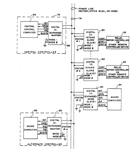
~: Referring now to FIG. 1, th~r~ is shown a
general block diagram of the co}nmunication nei:work
wherein a cen~ral con~roller indicated gen@rally a'c
76 can 'I:ransmit messages to and receive messages ~rom
20 a large number of remote stations over a conventional
power line indicate~ generally at 78. Tbe basic
building ~loc~ of the communication network is a
small, low cost diyital IC, indicated generally at 80,
which is arranged to ~ connected to the power line
25 7~ so that il: can receive messages from the central
controller at 76 and transmit messages to the central
eontroller over thi line.
The digi tal ` IC 80 is extr~mely versatile
and can be readily adapted to dif ferent modes of
30 ~ operation by simply establishing differen~ connec-
tion3 to two of tbe external pin~ of this device.
M~re particuiarly, as shown a~ remote ~tations ~1 and
#2 in FIG. 1, the di~it~l IC 8û may be pin configured
to op~rate in a ~tand alone ~lave mode in which it is
35 arrarl~ed to control ~n associated relay, motor con-
: troller or other relDote control device, indicat~d
~enerally at 82, by sendlng a control cutput si~nal
~ .
.~
,.
.: - . - -
. -- ~ . .. . ' ~ . -
., ,. , ' ~' ~ ' ' ; '
~-, ,
~4 ~ C~9~ 51930
(COUT)~ to the controlle~ device 82. In the stand
aione ~lave mode, the digital IC 80 can also respond
to an appYopriate command from the central controller
76 by tran!3mitting a mtssa~e back to the controller
76 over the power line 78 in which the sta~us of 2
ter~inal~ a~ociated with the controlled device 82~ -
identi~ied as STAT ~ and STAT 2, are given. Each of
the digi~al IC's 8~ i5 provided wi~h a 12 bit address
~ield so that as many as 4,0~5 of the devices 80 may
~e individually associated with different relays,
motor controllers, load management terminals, or
o~her controlled devices at location~ remote fro~ ~he
central controller 76 and can re~pon~ to ~bed lo~d or
- restore load commands transmitted over the power line
7~ by appropriately changing the potential on its
COUT line to the controLled device B2.
Th~ digital rc 8~ is also arranged ~o that
it ca~ be pin configured to operate in an expanded
slave mode as shown at station #3 in FIG. 1. In the
expanded sl2ve mode the digital IC is arranged to
respond to a particular command rom the central con-
troller 76 ~y establishing an interface with an as-
socia~ed microcomputer indicated qenera}ly at 84.
More particularly, ~he expande~ slave deYlce 80 re-
sponds to an enable interface instruction in a mes-
sage recelved rom the central controller 76 ~y pro-
ducing an ~n~e~rup~ ~ignal on ~he I~ line ~o the
mic~ocompu~r 84 and permitting ~he microcomput~r 84
to r~ad serial ~ata ou~ o~ a buffer shift register iR
3~ tbe digital IC R~ over the bi-directio~al D~TA line
in ~e~pon~e to serial clock pul es transmitted over
the SCK line from the microcomputer 84 to the digital
IC 80. The digital IC 80 is also capable of respond-
inq to a signal on the read write line ~RW) from the
microcomputer ~4 by loading..~erial data into ~he ~uf-
~er ~hif~ regi~ter in the dev1ce 80 ~ro~ the RAT~
line in coordination with serial cloc~ pul~e~ 5uppli-
. `,~,;
~' .
~'
15 ~ 9~ 51930
ed over the SCX line f rom the microcs;mputer 84 ~ Thedigital IC ao is then arranged to respond tc~ a change
in potential on the RW line by th e microcompu'cer ~
by incorpQr~ting the data suppl ied to it from the
5 microcomputzr 84 in a 33 ~it me-~sage which is format-
ted to include ~11 of the p~otocol of a ~tandard mes-
sage tran~mitted by the central controller 76. This
33 ~it message in the correce forma~ i~ then trans-
mitted by the IC 80 c~ver the power line 78 to the
10 central controller. As a result, the expand2d ~lave
device 80 enables bi~directional communication and
~ transf~r of data between the central corltroller 76
-: and the microcomputer 84 over the power line 78 in
response to a specific ena~le inter~ace in~ruction
lS initi~lly transmitted to the expanded Rlave device 80
from the central controller 76. nce the inter~ace
~as ~een established bet~een khe devices ~0 and 84
this inter~ace remains in effect until the digital IC
:' receives a message transmitted fr~n the c~n~ral con-
2û troller 76 which includes a disable interface in-
struction or the expanded slave device 8û r~ceive a
message from the central controller which irlclude5 a
command addressed to a dif ferent remo'ce station. In
either c~e the in'cerface between the network and the
25 microcompu'cer 84 is then disabled until another mes-
sage i~ transmitt~d from the cen~ral controller to
~: the expanded slave device 8~ wh~ch includes an ena~le
lnt~riEace in~truction. The expanded slave device 80
: al~o ~enads a busy signal over the ~3USY~ e ~:o the
30 mic~ocomputer 84 whenever 'che device 80 is receivirg
a message from the network 78 or transmitting a mes-
sage to the network 78. The BUSYN signal tells the
microcomputer 84 tha~ a message is being placed on
the nel:work 78 ~y the central con'croller 76 ev~n
35 though control of the ~uf~er shift register in ~he e~-
panded slave device ~û has been ~hifted to the micro-
compu~er 8 4 ~
:
16 ~ 9S 51930
The digital IC ~0 may also be pin conf igur-
ed to operate in an expanded master mode as indica~ed
at st~tion ~ 4 in FIG . 1. In the expanded master mode
the device ao is permanently interfaced with a mic~o-
5 compu~er 8~ so tha~ ~he microcQmputer 86 can opera~e
as an alternate controller and can send shed and re-
store load messages to any of the stand alone slaves
80 of the communication network. The microcomputsr
86 can also establish communicatios~ over the power
10 line 78 with the micrcomputer 84 through l:he expanded
slave IC device 80 at station ~3. To establi3~ Such
:: two way communica'cion, 'ch~ microcomputer 86 merely
transmits data to the expanded mast~r device 80 over
the bid~rectional DATA line which data includes the
15 addres o~ the exp~nded slave deY~c~ 80 at s'ca,tion ~ 3
and an enable interface instruction. The expanded
mas~er ~0 includeA ~his data in a 33 bit message for-
~: mat~ced in accordance with the protocol required ~y
the communication n~work and transmits this message
:
over the power line 7~ to the expanded slave 80 at
sta~ion #3. The expanded slave 80 a~ this station re-
sponds to the ena~le interface instruction by estai~-
~`~ lishing ttle above descri~ed i.nterface with the micro-
computer 84 after which the bidirec~ional exchange of
data ~etween 'che micrcomputers ~4 and 86 is made pO5-
~ sible in the mann~r described in detail heretofore.
:~ ~ A digital IC 80 which is pin configured to
ope~ate in the expanded master mode may also be used
a~ an interface between a central control computer
~8, which may comprise any microcomputer or main
~ramg computer, which is employed to control the re-
mote stations connected to the central controller 76
over the power line 78. Since each of the digital
IC's 80 puts out a BUSYN ~ignal to ~he associated
: 35 ccmput0r when i~ either receiving or transmitting a
me sage the pre~ent communication and control ~ystem
permits ~he use of multiple ~aster~ on the same
~.
. ,.
~ .
. ' . ~ ..
.
17 ~ 95 51930
network. Thu~, considering the central controller 76
and the alternate controller at station #4 which is
operating in the expanded mastec mode, each of these
ma~t~r~ will ~now when the other is ~ransmitting a
message by monitoring his BUSYN line.
It will thus ~e seen that the digital IC 80
i5 an extre~ely versatile device which can be u~ed as
either an addressa~le load controller with status
reply capa~ility in the stand alone slave mod2 or can
be used as either an addressable or non addre~a~le
interface ~etween the network and a microcomputer so
as to ena~le the bidirectional tran~mission of data
between any two ~icrocomputer control unit~ such as
the central controller 76 and th~ remote stations ~ 3
and #4.
All communications on the network 78 are
asynchronous in nature. The 33 bit message which the
digital IC ~0 is arranged to either transmit to the
network 7~ or receive from the ne~wor~s 7~ is speci-
fically designed to provide maximum ~ecurity and p~o-
tection against high noise levels on the power line
78 while at the same time making possible ~he estab-
lishment of interfac@s be~ween different microcompu
ter as descri~ed heretofore in connection with FIG.
1. The 33 bit mescag~ has the format ~hown in FIG. 2
wher~ln the 33 ~its B0-B32 are shown in the manner in
w~ic~ t~y are stored in the shi$t reqister in the
digital IC 80 i.e. reading from right to left with
the least significant bit on the extreme right. Each
33 ~it message begins with ~ start ~its B0 and al and
ends wlth 1 stop bit 832. Tbe start bits are defined
as logic ones "1" and the stop bi~ is defined as a
logic ~0". In the disclosed ccmmunication and con-
trol ~ystem a logic 1 is defined as carrier present
: and a logic 0 is define~ a~ the a~sence of ca~ie~
for any of the modulated carrier Daud rates.
, '. . ~ ' :
' " , . ,
.
18 3L~ 51930
The next ~it B2 in the 33 bit mes~age is a
control ~it which def ines the meaning of the sueceed-
ing ~e~sage bits B3 through ~26, which are referred
to a~ buf~r bits. A logic ~ control bit means
that the bu~fer bit~ cont in an addre s and an in-
struction for ~che dlg~tal IC 80 when i~ is conf igur-
ed to operate is~ either a stand alone slave moae or
an expanded slave mode. A logic ~OR controi bi~c B2
: ~ mean~ that 'the buffer b~ ts ~3 ~hroug~ B26 contain
data intended for an interaced microcomputes s~lcb as
the microcomputer 84 in FIG. 1.
The next four bi~ ~3-B~ af ~er the control
bit 2 are ins~ruction bits if and ollly if the pre-
ceeding control bit is a "i~ The instruction bits
B3 - ~6 can ~e decod~d to give a number of different
instructions to the digital IC 80 when operated in a
sl~ve mode, ei ther a ~tand alone s}a~e l~lode or an
~: expanded slave mode. The relationship betwe~n the
~: in~truction bits B3 - B6 and the corresponding in-
struction is shc~ n in FIG. 3. Referring to this
figure, when instructions bits ~3, ~4 and BS are all
: :: i'O~ a ~hed load instruction is indicated in which the
~.,
digital IC 80 re e~ its ~OUT pin, i.e. goes to logic
~ zero in the conventional sense 50 that the controlled
: ~ 25 device ~ is turne~ off. ~n X in ~it position B6
~; mean that the shed lo~d instruction will ~e executed
::~ independent~y ~of th~ value of the B6 bit. Hos~ ver,
if T~6 is a ~1~ the digital IC 80 will reply ~act: to
tbe ~ntral controller 76 with information regarding
the ~'catu~ o~ the lines STAT 1 and STAT 2 which it
recelv~ from the controlled device 82. The format
of the reply message is shown in FIG. 4, as will ~e
described in more detail hereinafter.
~ Wtlen instruction bits B3-B5 are 100 a re-
`:: 35 store load instruction is decoded in response to
which the digital IC ~0 3~t~ ita CO~ pin and pro-
vides a logic one on the COUq~ llne ~o the cont~olled
:'
~: .
''
- . . . .
. ~
19 51930
device 82. Here again, a "1" in the B6 bit instructs
the device 80 to reply back with statyus information
from the controlled device 82 to indicate that the
command has been carried out.
When the instruction bits B3-B5 are 110 an
enable interface instruction is decoded which in-
structs an expanded slave device, such as the device
80 at station #3, to establish an interface with an
associated microcomputer such as the microcomputer
84. The digital IC 80 responds to the enable inter-
face instruction by producing an interrupt signal on
the INT line after it has received a message from the
central controller 76 which contains the enable in-
terface instruction. Further operation of the digi-
tal IC 80 in establishing this interface will be de-
scribed in more detail hereinafter. In a similar
manner, the instruction 010 instructs the digital IC
80 to disable the interface to the microcomputer 84
so that this microcomputer cannot thereafter communi-
cate over the network 78 until the digital IC 80
again receives an enable interface instruction from
the central controller 76. In the disable interface
instruction a "1" in the B6 bit position indicates
that the expanded slave device 80 should transmit a
reply back to the central controller 76 which will
confirm to the central controller that the micro
interface has been disabled by the remote device 80.
The B6 bit for an enable interface instruction is
always zero so that the digital IC 80 will not trans-
mit back to the central controller data intended for
the microcomputer 84.
If bits B3-B5 are 001 a block shed instruc-
tion is decoded. The block shed instruction is in-
tended for stand alone slaves and when it is received
the stand alone slave ignores the four LSB's of
its address and executes a shed load operation.
Accordingly, the block shed instruction permits the
20 ~ 5i 51930
central controller to simultaneously control 16 stand
aione ~laves w~th a sin~le transmitted messaye so
that these slaves simultareously dis~ble their asso-
ci~ed contxolled d~vices. In a similar manner if
5 the instruction bits ~3-BS are 101 a ~lock restore
instruction is decoded which is simultaneously inter-
pret~d ~y 16 stand alone slaves ~o restore a load to
their respective controlled devices;. It will be
noted that in the bloc~ shed and bloc~ res~ore in-
10 structions the B6 bit must ~e 1-0'- in order for the
instructiorl to be execut2d. Thi is to prevent all
16 of the in tructed stand alone ~laY~s to attempt to
reply at the same time.
If the B3-BS bits are 011 a scram instruc-
15 tion is decodedD In response to the scram instruc:-
tion 311 stand alone slaves s:onr~ected to the networ~
78 disregard their entire address and execute a shed
}oad ope~ation. Accordingly, by transmit'cing a ~cram
~: instruction, the central controller 76 can simultane-
20 ously control all 4, 0~6 stand alone slaves to shed
their 1Oads in the event of an emergency. It will be
noted that ~he scram instruction can cnly ~ executed
when the B6 bit is a "on.
If the B3-B5 bits are all "1" a status in-
25 struction is decoded in which the addressed stand
alone slav~ talce5 no action with respect to its con-
trolled device but merely transmi ts baclt to the cen-
'cr~l con~roller 76 status informa'cion regardiny 'che
a~sociated controlled device 82.
Returning to the message bit format shown
in FIG. 2, when the received message is intended for
a ~tand alone slave, i.e. the control ~it is "1",
~its B10-B21 constitute address bits of ~he address
as~iglled to the stand alone slave. In 1;hi~ mode bits
35 B7-B9 and bits B22~2~ are not used. However, when
an enable in~erace instru::tion i~ given ~n the ex-
panded mode, bits B7 ~9 and B22-B26 may contain data
~ ,J
.
~q~
21 51930
inSended for the associated microcomputer 84 as will
be de-~ribed in more detail hereinafter.
8its B27-~31 of the received message con-
tain a five bit ac~ error checking code. This BC~
code is developed from the first 27 ~its of the 33
bit received message a~ the~e first 27 bits are
stored in its serial shift register. The stand alone
slave device 80 then compares its computed BCH error
code with the error code contained in bits B27 B31 of
:~ 10 the received message. If any bit~ of tbe BC~ error
code developed within the deviee 80 do not agree with
the coeresponding bits in the error code contained in
~its B27 B31 o~ the received message an .error in
transmi~sion is indicated and ~he device ~0 ignore~
- 15 the messa~e.
FIG. 4 shows ~he message ~rmat of the 33
~it me~sage whioh is ~ransmit~ed by the stand ~lone
s1ave 80 back ~o the ce~tral controller in respon~e
~ to a reply reque~t in the received message i.e. a "1"
-: 20 in the B5 bit posi~ion. The stand alone slave reply
message has the identical format of the received mes-
sage shown in FIG. 2 except that ~its B2S and B26
correspond to the status indication on STAT 1 and
STAT 2 lin~s ~eceived from the control device 82.
~-~ 25 ~owever, since B25 and B26 were not used in the re-
ceived me~sage whereas they are employed to transmit
~ information in th~ reply massage, the old BCH error
.~ che~king code of the received message cannot b~ used
: in tr~ns~itting a reply back to the central control-
ler. The stand alone slave device 80 re~omputes a
five bit BCH error code based on the first 27 bits of
the reply message shown in FIG. 4 as these bits are
being shipped out ~o the network 78. At the end of
the 27th bit of the reply message the new ~C~ error
: 3S code, which has been oomputed in the device 80 ~asad
on the condition of the sta~us ~it~ B25 an~ B2S, i~
then added on to the ~ransmi~ed message af~er which
:
,~
.
2 2 ~ 9~i 5 19 30
a stop ~it o O is added to complete the reply mes-
sa~e bac~ to the central controlJ.er.
Fiq. 5 shows the format of a second message
'cran~mi~eted ~o a digi'cal IC 80 operatin9 in an exp-
S anded mode, lt being assuming that the f irst messageincluded an ena~le interface as discussed previously.
In the format of Fig. 5 the control bit is ~0" which
informs all of the devices 80 on th power line 78
that the messaqe does not contain address and in-
10 struction. The nex'c 24 ~it~ after the contrc11 ~itcomprise data to be read out o~ the ~uf fer shift reg-
ister in the device ~0 ~y the as~ociate~ microt:wnpu-
ter S4.
In the illustrated embodiment the digital
IC 80 is housed in a 28 pin dual in line ~ackage.
Pre~errably it is cons~ructed from a f ive mic:ron
silicon gate CMOS ga~e array. A detailed signal and
~: pin a~signment o~ the deuice ao ls shown in FIG. 6.
It should ~e noted that some pins have a dual func-
tion. For example, a pln may have one function in
the stand alone slave conf iguratîon and anot~er func-
tion in an expanded mode configuration. The follow-
ing is a brief de~cription of ~he terminology as~ign-
: 25 ed to each of the pins o~ the device ~0 in FIG. 6.
TX-the transmit QUtpUt of the device ~0.
Trans~its a 33 bit message t~rough a suita~le coupl-
inq network to the common data line 78.
RX-the ceceive input of the device 80. All
~3 bit netwock transmissions enter ~he device through
thi5 pin.
RESTN-the active low power on reset input.
Rese'cs the internal registers in 'che device 80.
Vdd-~he power supply input of +5 volts.
V5!;-t~le ground referenc~.
:; XTALl and XTAL2 the cry9tal input~ . A
3.6a~4 mHz ~ 0.015~ crystal oscillator is required.
; ' ' .
: ,
` ~
.
9~
~3 51g30
~aud û and Baud l-the baud rate select in-
puts.
A0 ~A8 - the least: signif icant address ~it
pins .
S A9/CLK - dual function pin~ In all ~ut the
test mode~ ~his pin i~ ~he A9 address inpu~ pin. In
the test mode this pin is the clock ~tro~e output of
the digital demodulatox in the device 80.
Alû~DEMOD - a dual function pin. In all
but the test mode thi~ pin is the A10 address input pin.
Ir~ ttle tes~ mod~ ~his pir~ i~ the demodul~ted Qu~put
(DEMOD) of the digital demodulator in the device 80.
All/CD - a dual function pinu In al} put
the 'ce~t mode this pin is the All address input p~n.
In the test mode this pin i~ th~ receive word detect
output (C~) of ~he diqi~al demodula~or in the devioe ao.
:~ BUSYN/COUT - a dual function output pin.
In the expanded slave or expanded mas'cer modes this
pin is the BUSYtl ou~put of the micro interface. In
the ~tand alone slave mode this pin is ~he switch
cont rol ou tput (COUT ) .
INT/TOUT ~ a dual function output Pin. In
the expanded ma~er or expanded slave modes this pin
is the interrup~ output (INT) of the micro inl:erface.
In the stand alone slave mode this pin is a ~:imer
control pin (TOVq ) .
8CIC/5TATl - a dual functlon input pin. In
he expanded master and expanded slave modes this pin
i~ the serial clocl~ (SCK ) of the micro interace ~ In
the ~tand alone slave ~node it is one of 'che two
status inputs (STATl ) .
RW/STAT2 - a dual function input pin. In
the expanded master or expanded slave mode this pin
i~ the re~d-wri~e control line of the micro in~er-
face ~R~)o In the st~nd alone slave it is one of the
two ~tatu~ inputs (STA~2).
:~'` . .
~: .. ;,
~8~9~
24 51g30
D~TA/TIMR - a dual ~unctiorl pin. In the
expand~d ma~ter or expanded slave mode~ this pin i5
~he bidirectional data pin ~DATA) of t:he micro inter-
face. Ir the stand alone slave mode thi~ pin is a
s timer control line (TIMRJ.
All input pins of the device 80 are pulled
up to the +S f ive volt supply Vd,d by int~rn~l 10k
pull-up resistors. Preferably these internal pull-up
resistor~ are provided ~y suita~ly l~ia~ed tran~i~tors
10 within the device ~0, as will be read$1y understood
by those skilled in the art.
As discussed generally heretoiEor~ th~ d~qi-
- tal IC ~0 is capa~le of opexation in ~everal differ-
ent operating modes by simply changing ex'cernal s:on-
15 nections to the device. The pins which control the
modes sf operation oE the device 80 are pin 1 and
2~, identiied as mode 1 and mod! 2. The relat:iosl-
ship between these pins and the selected mode iY as
f ol lc)ws:
:~ 20 MODE 1 MODE 0 SE~ CTED MODE
: ~` 0 O ~xpanded slave
0 1 stand alone slave
1 û expanded master
tes t
. ~ ~ 25 When only the MODE 1 pin i5 grounded the
MOD}5 0 pin as~ume~ a logic "1" due to it~ internal
- pUll Up r~8i5~0r and the digital IC 80 is opera~ed in
the ~t~nd alone s}ave mode. In this pin conf igura-
tiorl the di~i~cal IS 80 acts as a switch control with
st~tu~ ~e~d ~ackO The device 80 . ontains a 12 ~it
addre~s, a ~witch control output (COUT~ and two
status inputs (STATl) and (STAT2). The addressed
device 80 may be commanded ~o ~et or re-Qet the switch
control pin COUT, reply with ~ta~us information from
: ~ 35 it~ two ~ atus pin~, Ol: both. The devic~s ~0 ~ay be
addres3ed in blocks of 16 fos one way ~w~ tch cont~ol
'~ commands~
.
39~
25 519~0
When both the MODE 1 and MOD~ 0 pins are
~rounded the d~vice 8 ls operated in an expanded
sl~e mode. In this pir conf igura~;ion the device 80
cont~ins a 12 bit addres and a microcompu~er inter
face. Thi~ in~erface allows the central corltroller
76 and a microcomputer 84 tied ts:~ the device 80 to
communicate wi~h each other . The interf ace is dis-
a~led until the cen'cral cont~oller 76 ena~le~ it by
sending an enable interface command to t:he addressed
digital IC f~OD The central controller and ~nicrocom-
puter communicate by loading a seria.L shift regiRt~r
in the digital device 80. The central controller
does this by sending a 33 bit messa~e to 'che device
~0 . This causes the microcomputer interf ace ~co in-
Serrupt the microcomputer 84 allowing it to read 'che
shif t register . The microcomputer 84 communicate~
with the central controller - 76 by loading the same
shif t regis~cer and commanding the device 80 to trans-
mit it onto the networ~. :
When only ~che mode 0 pin is grounded the
MODE 1 pin as~umes a 1O9ic "1" due to its internal
pull up resistor and the device 80 is operated in the
exp~nded master mode. In ~iis mode the d~vice 80
operatPs exactly like ~he expanded slave mode except
that the micro interface is always- ena~led~ Any net-
work tran~mi~sions tha~ the digital device 80 receives
. produce itlt~rrupts ~o the att ched microcomputer 84,
en~b~Ling it ~o read the serial shift regis~cer of the
device 80. Also the microcornputer may place data in
the ~hlfe register and fo~ce the device 80 to trans-
mit onto the network at any time.
iahen both the MODE 1 and ~IODE 0 pins are
ungrounded they assume "logic" values of 'l" and the
devi~e 80 is conf igured in a t~st mode in which some
of the ex~ernal signals in the digital demodulator
portlon o~ ~he device 80 are brough~ out to pin for
te~c purposes, as will be d~cribed in more detail.
.
3L~B10~7S
2~ 51g30
As discussed generally heretofore the digi-
tal IC.aO is adapted to transmit messages to arld re-
ceive me sages from different types of communicatior~
network l$nes such as a conventional power line, a
S dedlcated twisted pair, or over fiber optic cables. When
the digital IC 80 i~ to work with a cons entional AC
power line 78, this device is pin configured so that
it receives and transmits data at a baud rate of 300
~i~s per second. Thus, for power line applications
the ~inary ~its consist of a carri.er of 115.,2 kE~z
which is modulated ~y on-off keying at a 300 ~aud
bit rate. This bit rate is chosen to minirlize bit
error ra~s in the relatively noi~y environ~oent Of
the power line 7~. Thus, for power line application
the digital IC ~0 is configured as shown in PIG. 7
wherein the baud 0 and ~aud 1 pin~ of the d~vice 8û
are ungrounded and assume logic values of ~1" due to
their internal pull up resistors. The RX and TX pins
of the devlce 80 are coupled througtl a coupling net-
work and ~mplif ier limiter 90 to the power lines 78,
thi~ couplin~ network providing the desi~ed i~ola~ion
~etween transmit and received messages so ~hat two
way communication between the digital IC 80 and 'che
power line 7~ permitted, as will be described in
more detail hereinafter. When the device 80 is pin
configured as shown in FIG. 7 it is internally ad-
ju~t~d so that it will receiv~ modulated carrier mes-
sag~s at a 300 ~aud rate. It is also internally con-
~ trolled so that it will tr~nsmit messages at this
-: 30 same 300 ~aud ra~e.
- In Fig. 8 the digital IC ~0 i5 illustrat-
~<:1 in connection wi~h a communication networ~c ir
which the common data line iq a dedicated twisted
pair 92. Under these condi~ions the baud 0 pin of
3S the device 80 is groundea whereas the baud 1 pin as-
5ume9 a lQgiC value of ~1~ due to its internal pull
up re~istor . When the device 80 i s pin conÇi~ured as
9~:i
27 51930
shown in FIG. a it i~ arranged to transmit and re-
c~lve modulat~d carrier messages at a 1200 baud rate.
The 1200 b~ud bit rate is pos~ible due to the less
noi y environment on the twisted pair 92. In the
S configuration of Fig. 8 the coupling network 90 is
al~o required to couple the device 80 to the twisted
p~i~ 92.
For high speed data communication the digi~
tal IC ao i5 also pin configura~le to transmit and
receive unmodulated data at the rel~tively high ~it
rate of 38.4R ~aud. Whe~ so configured the device 80
is particularly 5uita~1e for ope~ation in a CO~mUQi-
cations system whih employ~ the fiber optic c~les
94 tFi9. 9) as the communication network medium.
lS More particularly, when the dev~ce 80 is to function
with the fi~er optic cables 94 the ~aud 1 terminal is
- grou~ded and ~he ~aud 0 ~ermi~al assumes a logic
value of "1" due to its in~ernal pull up re~istor, a
~ shown in ~G. 9. In the fiber optic cable system of
- 20 FIG. 9 the coupling network 90 is not employed.
:~ Instead, the receive pin RX of th~ device 80 is
directly co~nected to ~h~ output of a fi~er optic
receiver 96 and the ~ransmit pin TX is connected to a
~: fi~er optic transmitter 9 A digital IC ~0 in the
central controller 76 is also interconnected with
the fiber optic cables 94 ~y a suita~le transmitter
r~ceiver palr lO0. The fiber optic receiver 96 and
tran~mitter 98 m~y comprise any suita~le arrangement
in w~ich the RX terminal is connected to a suita~le
:: 30 phot~de~ector and amplifier arrangement and the TX
~ermin~l is connccted to a suita~le modulated light
source, such as a photodiode. For example, the
Hewlett Packard ~BR-lS01/2502 transmitter receiver
pair may ~e employed to connect the àigital IC 8û to
~- 35 the f iber optic ca~le~ 94. Such a ~ran~mitter
receiver pair operate~ a~ TTL co~pati~le logic level~
;
.
' ~' ' ~ ' '
rl95
28 51930
whieh ar~ ~atisactory for direct application to the
RX al~d.TX termina1s O]~ the device 80. ;~
In Fig. 10 a typical conf iguration i5 shown
for the device 80 when operated in the ~tand alon~
~lava mode . Re~err ing to thi~ f igure, plu3 5 volts
DC i8 applied ~o the Vdd termina1 and the V5~ terminal
is grounded. A crysta1 102 operating a~ 3.6864 -0.015%
mHz is connected to the OSC1 and OSC2 pinæ of the de-
vice 80. Each side of the cryska1 is connected to
ground thro :3h a cap~citor 104 and 106 and a r~iato
108 is connected across the ~ry~tal 102. Prefer-
rably, ~he capacitors 104, 106 have a value of 33
picofarads and the resi~or 10~ ha!~ a value of 10
megohms~ The ~aud rate at which the devic~ 80 i~, to
operate can be se1ected by me~ns of the baud rate
switches L10. In the em~odiment of FIG. 10 these
switches are open which mean~ that the device 80 i~
operating at a baud rate of 300 ~aud which i sllit-
able fo~ powe~ 1ine network cc~mmunication. The MODE
1 terminal is ~rounded and the MODE 0 ter;ainal is not
-~ conn~cted 50 that the device 80 is operating in a
stand alone s1ave mode. A 0.1 micrc3farad capacitor
112 is connected to the RESETN pin of 'che device 8û.
~ 25 When power is applied l:o 'che Vdd terminal of the device 80
: ~ the capacitor 112 cannot charge immediate1y and hence
~- provide~ a re~e'c igna1 of n o" which is employed to
-~ re~et var~ou~ 1Ogic circuits in the digital IC 80~
A1~o, a power on reset signa1 force~ the COUT outpu'c
of the device 80 'co a logic nll-. As a re u1t, the
contro11ed devi~e, ~uch a~ the relay coi1 11~, is en-
ergized through the indicat,ed transistor 116 whenever
powex i~ applied to the digital IC: 80. The condition
of the relay 114 is indicated t~y the status info~ma-
tion switches 118 which are opened or closed in
acccrd2nce with the s$gn~1 3upp1ied to ~he con~rolled
relay 114 . ~wo ~eeeo~ ~n~o~m~elon swltches are pcO-
9~
29 51930
vlded for the two line5 STAT1 and STPT2 even though
only ~.~in~l~ device is controlled over the COUT con- 5
trol llne. Accordingly, one status line can be
ct)nn~cted to th~ COUT line to conf irm that the COUT
sigr~al was ~ctually developed and the other ~tatus
line can be c:onnected to auxiliary contactt~ on the
relay 114 to conf irn~ that the load in~truction has
actually been exeeut~d.
A series of twelve address ~wi'cches 120 may
~e selectively connected to the address pins Aû-All
so as to provlde a digital input 3ignal to the
address comparison cire:ut in the digital ~C ~0. Atly
address pin which i~ ungrc)unded by the sw~tcho~ 120
a~sumes a logic ~1" value inside ~he devic:e ~0
through the use of internal pull up re~istors on e~ch
address pin. In this connection it will be under~tood
that the device 80, and the external components a~-
:~ sociated with ié, includ~ng the coupling neéwork 90
m~y a~l be assembled on a small PC b~ard o~ ca~:d
~: ~ 20 which can be associated directiy with the~ controlled
device such as the relay 114. Fur~hermore, the digi-
tal IC 80 and its assoc:iated components can be o ex-
tremely small si2e so that it can be actually located
in the hou~iag o~ the device which it controls.
-~ 25 Thus, i~ the device 80 i5 employed to control a relay
for a ho'e w~ter heater or reezer in a resid@nce, it
~: ~ may be a~oc~ted directly with such relay and re-
ce~ve me sage~ for controlling th~ relay over the
hou~ wirinq of the re~dence. If the controlled de-
vice does rlo~ include a f ive volt source for powering
the digital IC ~0, ~he coupling network 90 may pro-
~tide ~uch power directly fran the power line 78, as
will be de~cr$bed in more detail hereinafter.
In some situa~ion~ it i8 desi~aDle to pro-
vide a variably tim~a ~hed loa~ feature ~or particu-
lar ~tand alone ~lave ~pplication. For example, ~f
the digit~l IC ~0 i~ employed to control a hot water
:`
: , ,
.
.
. , ` ~
l~B~095
30 51930
heater or freezer, it may be controlled from a cen-
tral controller so that the freezer or hot water
heater may be turned off (shed loa~ instrUCtionJ dur-
ing p~k lo~d period~ in accordance with predeter~in~
S ed time Qchedules. Under these conditions it would
be desirable to provide a variahly tim~d facili~y for
restoring power to the controlled freezer or hot
~ater heater in the event that the central controller
did no~ transmit a message instructing the digital IC
~0 to restore load. ~uch a Yaria~:Ly eim~d ~hed load
feature may be provided in a ~imple manner by
employing the arrangement shown in FIG. 11 wherein a
variable timer 130 is associated with the digital IC
80. The varia~l~ timer 130 may compri~e a commercial
lS ~ype MC14536 device which is manufactured by Mo~orola
Inc and others.
In the arrangement of FIG. 11 the COUT line
o~ ~he digital IC 80 is connected to the reset pin of
the variable timer 130 and i5 also connec~ed to an
internal NOR gate U625 of the device 80 whose output
~: is inver'ced. The TOUT output line of the device 80
is connected to the cloclt inhibit pin of the ~imer
130 and ~he decode outpu~ pin of this timer is
~: connected to the TIMR input pin of the device 80.
The devic~ 80 in Pig. 11 is also conencted in the
stand alon~ slave mode of F~G. 13 in which mode the
TOUT and TIMR linec are enabled. In the embodiment
of FIG. 11 the cor~trolled relay 114 is connected to
tb~ TOUT line rather than to the COUT pin of the
dev~ce 80. The timer 130 has an internal cloc~ whose
requency can be de~ermined by ~he external resistors
132 and 134, and the capacitor 136 as will be readily
under~tood by those skilled in the art. In addition,
the t~mer 130 has a number of ~im~r input termin~7 q
A, ~, C and D to which shed time Qelect switches 13~
may ~e s~lectively connected to e3ta~ h a de-~ired
vari~ timer interval.
. . .
C~9~;
31 51930
When power is applied to the digit~l IC 80
in FIG. 11 a power on reset produces a logic ~ re-
store load state) on the COUT pin. This signal is
applied to the reset terminal of the timer 130 forc-
ing ~he ~imer ~o reset and its decode output pin low.
This decode output pin is connected to the TIMR line
of the device 80 wbich is internally connected to the
NOR gate U625. Since the TOUT pin is the logical OR
of COUT and the decode output o~ the timer 130, upon
power on reset TOUT is a logic 1 and the relay 114 i5
in a restore load state. When the COUT line is re
set, in response to a shed load in truction to the
device 80, the timer 130 is allowed to ~tart counting
and the T:)UT pin is a logic "0" Gausing the load to
l; ~e shed. When the timer 130 counts up to a num~er
determined by the shed time selec~ switches 138 its
decode out pin goes high forcing TOUT high i.e. ~ack
to the res~ore load state and inhi~iting tbe 'ci.m~r
. cloc~t. Accordingly, if the central controller for-
get~ ~o restore load to the relay 114 ~y means o~ a
; network message transmitted to the devic~ 80, the
timer 130 will restore load automatically after a
p~ed~termined time interval.
. In FIG. 12 the main component parts of the
digital IC 80 are shown in bloc~ diagram form when
the device 80 is operated in the stand alone slave
mode and i~ arranged to receive a message transmitted
over the network 7~ which includes a shed load in-
~truction. The incoming message is amplified and
~- 30 limited in the coupling networ~ 90, as will ~e de-
-~ scribed in more detaiL hereinafter, and is applied to
the RX terminal (pin 6) of the digital IC 30. It
;~ will be understood that the incoming message is a 33
~ bit message signal having the format descri~ed in de-
: 35 eail heretofore in connec~ion with FLg. 2. This in-
coming message is demodula~ed in a dlgital demodu-
lator 150 whicn also includes the start bit detection
.~:
. .
:
':;
8~9~
32 5 l9 30
and f~amir!g logic necessary to esta~ h the bi~ in-
terval~ o~ the incoming asynchronous message trans-
mitted to the device 80 over the network 7~. The
dig~ta:l. demodulator and its accQ~npanyirlg frasning
S logic will ~e descri~ed in more detail hereinafter in
connection with a description of the detailed ~chema-
tlc diagraslt o~ the device 80 shown in FIGS. 18 to 33D
~ he ou~put of the demodulator 150 is s~ap-
plied to a serial shift re~ister indicated generally
lO at 152~ The serial shift regis~er 152 comprises a
series of 26 ieria~ly corsnected sta~e~ th@ first 24 of
which are identif ied as a buff~r and qtore bit~ ~33-
B26 (Fig . 2 ) o~ the teceived me~sag~ . The next stage
is the control bit register U528 which stores the
15 control bit B2 (Fig. 2) of the received m~ssag~. The
- final ~tage of the serial shift regi~ter 152 is a
start ~its re~ister U641 which 5tore3 I:~it5 ~3 arad ~l
(Fiq. 2) of the received messa~e. In this connection
it will ~e recalled tha~ the two sta~t ~its B0 and ~l
20 of eactl message bo~h have a logic value of '1" and
hence constitute a carrier signal which extends over
two ~it intervals so 'chat both bits may be registered
in the single re~i ter U641. In this connection it
should be noted that all logic components having U
25 numbers r~fe~ to the correspond-ing logic elernent
shown in detail isl the overall schema~cic of the digi-
tal IC 80 ~hown ir FI:;S. 18 to 33. The serial shift
r~gi~ter 152 i3 loaded ~rom the iefe ~y the demodu-
~: lated O~ltpUt of the demodulator 150 which is applied
30 to the data input of ~he register lS2, this data ~e-
ing cloc~ed into the register 150 ~y means of ~uf fer
shift clock pulses (BSHECLK) developed by the demodu-
la~or 150 at the end of each ~it inte~val in a manner
d~scribed in more detail hereinaf ter . Accordingly,
3S the inooming message is shifted through the register
152 until th~ ~tar~ bit3 reg1ster U64~. is ~et ~y the
two ~tart ~its B0 and Bl to a logic ~l" value. In
, . . . . .
', ~
':
33 51930
this connection il: will De noted that the ~its of the
incoming me~3ag~ a~e tored in the Duf fer portion of
the regi3ter 152 in the manner shown in FIG. 2 with
the lea~e signlf icant bit B3 stored in the regaster
5 next to ~he con~rol ~it register U528.
A~ the demodula~ed data ~it~ are thus being
loaded into ~erlal ~hift register 152 they are also
simultaneously supplied to a Bt::~ error code computer
indica'ced g~nerally at 154. More particularly, the
10 DEMOD output of the demodulator 150 is supplied
through a swi tch 156 to the input of the BC~ error
code computer 154 and the output of this compute~ is
connec~ced to a recirculating input through the swit~h
158. The BCH error code compu~er 154 compris~ a
15 series of 5 serially connected shift register s~ages
and when 'che witches 156 and 158 are in th~ ition
shs:~wn in FIG. 12 the: comp~ter 154 ::~putes a 5 ~it
error code based on the first 27 me sage ~it~ which
it receives from the demodulator 150 as thes~ ~its
20 are i~eing stored in the serial shi~t regiqter 152.
The ~lock puls~s on the BSHFCLE~ line, whic:h
are used to advance the s@rial shift regi~ter 152,
are also ~upplied to a message bit coun~r 160. The
-; coun~er 160 is a ~ix tage counter which develops an
25 output on i~s ~nd-of word (EOW) output line when it
counts up to 32. In this connection it will ~e
noted that by u~ing two logic "1" start bits which
are counted a~ one, the total message length may be
count~d by digital lo~ic while providing increased
30 noi~e immunity ~y virtue of the longer start bit in-
terv~l .
The message bi t counter 160 also sets a
la~ch at the end of the 26th me3~age ~it and devel-
opes an enabling signal on its GT26 (greater than 26)
35 output line. The GT26 slgnal controlq the 3witches
156 and 15~ ~o that after the 26th messag~ b~ the
DEMOD output oE the demodulator lS0 i~ ~upplied to a
.,.
, . ..
.
g~
34 51930
BCH cor~para~cor 16? to which GOmparator the output of
the ~C~ erLor code computer 154 is also qupplied. At
the ~ame ~ime ~h@ witch 158 is opened by the GT 26
sigr.al so that the BCH error code computed in the com-
5 puter 154 res~ains f ixed at a value corre ponding tothe fir~t 26 bits of the received message. Since the
demodulator l5û continues to supply BSHFCLR pulses to
the computer 154, ~e 8C~ error code developed ir; the
computer 154 is then shifted ou~ and compared bit by
10 ~it with t~e next 5 ~its of the received me3sage i.e.
827-B31 (Fig. 21 wh~ch con~titute t11e BCB error code
portion of the incoming received message ~nd ar~ -~up-
plied to the other input o1~ the BCH comparator 162.
If all five bits of th~ BC~ error code computed in
15 the computer 154 correspond with the f ive bits of ~he
BCE~ error code con~ained in ~its ~27-B31 of the re~
ceived message the comparator 162 develops an output
~: on its ~CHOK outpu~ ~ine.
The dig~cal IC ~0 al50 if~cludes ~n add~ess
20 decoder indicated generally at 164 which compeises a
series of 12 exclusive OR ga~es and assc)ciated logic.
It will ~e recalled fro~n the previous description of
FIG. 2 that bits Bll-B22 of a received message con-
tain an address corresponding to the particolar stand
25 alone slave with which the central controller wishes
to communica~e. Al~o, it will be recalled from the
preceeding descrip~ion of FIG. 10 that the address
~eleGt ~witches 120 are connected ~co th~ address pins
A0-All of the digi tal IC 80 in accocdance wi th the
30 addre s ~ssigned to eac~ particular stand alone
slave. The address decoder 164 compares the setting
of the address select switches 120 with the address
stored in bit~ Bll-B22 of the ~u~fer portion o~ the
serial shi~t regi~2ter 152. If the two addres~es co-
35 incide the decoder 164 develope~ an output on its ad-
dress O~t ~ADDCIK~ outpu'c line.
51930
rhe digi~al IC ~0 also includes an instruc-
tion decoder 166 which decode5 the output~ of the
buff~r ~age corresponding to bit, a3-B6 (Fig. 2)
whlch contain the instructior. which the addressed
5 stand alone slave is to exeoute. Assuming that ~its
B3-B5 all have a logic value of "O", a shed load in
struction is de~oded, as shown in FIG. 3, and tbe in-
~tructis:)n decoder 166 produces an output on its shed
load 1 i ne ( SHEI)N ) .
As discussed generally hecetofo~e, the conW
trol ~it B2 of a message intended or a ~tand alone
slave alwas!~s has a logic value of "1" lndicatinsl th~t
bits ~3-B26 of this message include addre3s ~its and
instruction bits which are to ~e compared and decoded
Ln the de~oders 164, 166 of the digital IC 80. When
the control bit register U52~ in the seEial shift
register 152 is se~ an enal~ling ~ignal is supplied
over the C3N~ROL output line of the register US28 to
the execute Logic circuits 1700 The BCHOK output
~0 line of the comparator 162, ~he EOW output line of
the ntes~age bit counter 160 and the ADDOK output line
of the address decoder 164 are also supplied to the
execute logic circuits 170. Aceordingly, when the
message ~it counter 16~ indicates that the end of the
message has been reached, the comparator 162 indi-
cates that all bi~cs of the received BC}I er~or code
agreed with the *rror code computed by the comp-~ter
154, the addres~ decoder 164 indicates that the mes-
~age i3 intended for this particular stand alone
slave, and the control bit register U52~3 is set, the
loqic circuitC 170 develop an output signal on the
EXECUTE line which is anded with the SHEDN output of
: the instruction decoder in the NAND gate U64~ the
output of which is employed to re~et a shed load
la~ch U651 and U6~2 so tha~ ~:he COUT output pin of
the ditigal IC 80 goes to a logic: value of l-OU and
pow~r is removed rom the controlled device ~2 (Fig.
36 51930
1). The stand alone slave thus executes the instruc-
tion c~ntained in the received messaye to shed the
load of the controlled device 82. As discussed gen-
erally heretofore when power is applied to the digi-
tal IC ao the shed load latch is initially reset ~ythe signal appearing on the PONN line so that the
COUT line goes high when ~5v. power is applied to the
device 80.
When the message ~it B6 (Fig~ 3~ has a
logic value of nl~ the ~tand alon~ slave not only
executes a ~hed load instruction in the mann~r de-
scribed in connection with FIG. 12 ~ut also is ar~
- ranged to transmit a reply message bac~ to the cen-
tral controller as shown in FIG. 4. In this reply,
lS message bits B25 and B26 contain ~he two 3tatu9 in-
puts STATl and STAT2 which appear on pi~s 26 and 25,
: respectiv~ly, o~ t~e digital IC ~0. Consldered very
generally, this reply message i5 developed by hi~t-
ing out the data which has been store~ i~ the serial
20 shift register 152 and employing this data to on-off
~ey a 115.~ k~2 carrier which i5 then ~upplied to tne
TX output pin of the device 80. ~owever, in accord-
ance with an important aspect of the disclosed
system, the status signals appearing on the STAT 1
and STAT 2 inpu pins of the deviee ao, which repre-
sent the condition of the controlled relay, are not
e~ployed to ~et the status bits B25 and B26 of the
reply ~essage until after 15 bits have been read ou~
o the seri~l shif t register 152. Thi~ gives con~id-
erable ti~e ~or the relay contacts to settle down be-
fore their tatus is added to ~he reply me~sage being
transmi~ted back to the central controller.
In Fig. 13 the operation of the qtand alone
lave in formatting ~nd transmitting such a reply
message back to the central controller i shown in
block diagram form~ Referr~ng to thi~ figure, it is
a3~u~ed tha~ a message ha~ been received from the
:
3~i
37 51930
c~ntral c:ontroller and has been stored ira the serial
3hift ~egist~r 152 in the manner descri~ed in detail
he~o~o~ore in connection wi~h Fig. 12. It is further
a ~ ed that the control bit ~2 of the received mes-
~age has a logic value of "1" and that the mes~age
bit B6 stored in the ~uf fer portion of th~ register
152 has a logic value "1" g~hich ins~ructs the ~tand
alone slave to transmit a reply message ~ac~ to the
central controller. When the B6 bi~ has a hl" value
the instruction decoder 156 produce an outpuS ~lgnal
on its COM 3 output line. A~so, at the end o~ the
received message the execute logic circ~it~ 170 (~ee
Fig. 12) produce an EXECUTE ~ignal wh~rl the corld~-
tions descri~ed in detail heretofore in connectior
with FigO 12 occur. When ~n EX~CUTE signal i5 pro-
duced a reply latch 172 proYidea an output which is
employed to set a sta~us latch 17~. The ~tatus la1:ch
174 provide~ a contr~l signal to the status control
logic 176. However, the condition of the ~tatus pins
STAT 1 and STAT 2 is not emplGyed to set c:orrespond-
ing stages of the buffer portion of the serial shift
register 152 until af ter lS ~its have ~een shifted
: ~ out of the register 152. At that time th~ message
~it counter 160 provides an outpu~ on its "lS" output
~: 25 line which is employed in ~he status control logic
176 to ~et the corresponding stages of ~he ~uf fer
portion o~ the register 152, these stages correspond-
. ;~ ing to the location of bits B25 and B26 in the reply
m~sage after 15 bits have been shifted out of the
reg~ster 152.
Con~idering now the manner in which the re-
ceived message which has been stored in the ser~al
shi~t register 152 i~ shifted out to form a reply
~e3sage, it wil} be recalled that a message which is
tran~mi~ted over the ne~cwork ~8 requires two star~
bits h~ving a logic value of ~ owever ~ when the
message was re::eiv~d it was initially det~c~ced by de-
38 51930
tec~ing the pre~ence of carrier on the network 7~ for
a dura~ion o 2 bit~ and, hence, the two start bits
o~ the r~cei~ed mes~age are ~tored as a single 5it in
th~ ~t~rt bits regi~ter U641. When a reply message
~:: 5 i~ to be tran mitted over the networ~ it is necessary
ts~ provide a modulated c~rr ier of two ~it3 duration
in resporlse to th~ single star~ ~it ~tored in the se-
:~ gi~ter U6410 To accomplish 'chis, a transmit ~trobe
- ~ signal ~TXSTB) is derived frs~m ehe reply latch 172
and is coupled through l:he NOR gate U601 to reset a
one bit delay flip-flop 178 which ha~ it~ D input
connected to the f ive volt ~3upply ~dd . As a re~ult
th~ S2N ou~put of the flip~ p l~B i~ invert~dl to
provide a transmit ~tro~e A (TXSTBA) ~ignal which
sets a transmit control }atch 180. Wb~n the latch
180 L~; 3et it provides a tran mit on t~XONN) signal
:` which is employed to relea~e ~ch~ ~raming counter3 in
l:he demodula~or 150 so that they ~gin to provide
13SHFCLR pulses at on~ bit irlterv~ls .
` ~ 20 For the f irs~ 26 ~i~s o the reply message
:~ the output of the star'c bits regi$t~r U641 is con-
nected throuigh a swi~ch 190 ~o a transmit fl~p-flop
182 whic~ is also ~et by the TXSTBA signal and is
held in a set condition ~o that it doe~ not respond
~o the f irst BSHFCLK pul~e whictl is applied to its
clock input. At the sam~ time the QN output of the
one bit delay flip-flop 178 is com~ined with the
f l~t ESS~FC:~ pul~e ln the NA~D ga~e U668 ~o as to
~ p~oY~de ~ ignal which set~ a t~ansmit enable Latch
184. When the transmit enable latch 184 is ~e~. it
pro~des an enabling signal to the modulator 1~6 to
wh~ch is al~o supplied a carrie~ signal having a fre-
quency of 115 . 2 ~Iz~ f~om the digital demodulator
150. When th~ tran~mit flip-flop 1~2 i~ initi~lly
3S ~et by the TXS113A line going low, i~ provides a 1 on
its Q outpu'c to the ~odulator 181j. Accs)rd~ngly, when
the trans~it ena~le latch 18~ provide~ an enabling
, ~ .
.~ :
.. . .~ . .
.. , . . :
., ~ ..
o~
39 51930
~ignal to the modulator 186 a carrier sutput i~ up-
plied to tne TX outpu~ pin o~ the device 80 and i5
supplied to ~he ne~wo~ 78. During this initial
tran~mis~on o carrie~ durin~ ~he ~irst start bi~
5 inServal th~ data in the serial shift reg~st~r 152 is
not ~hi f ted out because BSHFC~ pul~e~ to 'che cloc~
input of the regi ter 152 are ~locked by th~ NAND
ga~e U697. The NAND gate U697 has a it~ second input
a signal from the GT26N output lin~ o~ the me saqe ~it
counter 160 which is high until 26 ~its hav~ been
shifted out of the reglster lS2. Hows!~vez, a ~hird
input t~ the NAND gate U697 i~ the lrxsTB~ llne whlch
went low wh~n the 1 bit delay f~ip-flop 178 wa3 ~e-
set. Accordingly, the first ~SHFCLK pulse i~ not ap-
15 plied to the cloc~ inpu~c of the regi~er lS2 2l1though
this pulse~ does set the transmi~ ENA}3~E latch 184 and
enable carrier ou~put to be suppl~d to th~ TX outpu~
pin for the f irst bit interval. However, a shor~e in-
- terval after the first BS~FCLK pulse, a delayed shif~
20 clock pul~e (DSHFE~CLR), which is also developed in
~:he framing logic of the demodulator 150, i~ ~upplied
to the clock input of the 1 ~it delay flip-flop 178
'chat the TXSTBA line qoes high shortly after 'che
~irst BS~E~LR pulse occurs. When the TXST~A line
25 goes higb the BSE~ K pulses pa~s through the NAND
gate U697 and shift data out of 'che register 152 and
the ~e~ially connected transmit f lip-f lop 1~2 to the
tnodulator 186 ~o tha'c the ~ingle ~car~ bit stored in
th~ register U64ï and the remaining bits i32-~6 of
30 th~ recei~ted message con'crol the modulatio~ of the
ca~rier suppl~d to the TX output pirl. In this
connection it will be noted that th~ 3SHFCLK pu152s
ar~ al~o supplied to 'che clock input of the tran~mit
flip-10p 182 so as to permit the ~erial shift of
35 data to ~he TX ola~put pin. Howev~r, a~ di~cu sed
~bove, wh~n the TXST~P~ 1 ine i ~ low i t hold~ th~ f 1 ip-
- :
,
~8~l~9~
51930
flop 182 ~et so that it doe~ not respond to the first
BS~FCLR pulse.
Considesing now the man..er in ~hich the
STA~ 1 and STAT 2 s~atus 5ignals from ~he controlled
device are added to ~he reply message, it will be re-
called that the bufer stage~ are not set in accord-
ance witb the sign~ls on the ST~T 1 and STAT ~ pins
until 15 ~i~s have ~een snifted out of the regis~er
152 in order ~o allow time ~or the relay con~acts of
the controlled device to assume a final po~ition. It
will al~o be recalled that the B25 and B26 bits of
the r~ceived message are reserved for ~tatus ~its to
~e added in a reply message ~o tha~ the las~ active
bit in ~he received message is B~4. When the B24 bit
: 15 has been shifted 15 times it appears in the B9 stage
of the ~uffer portion of the serial s~ift register
152. Accordingly, the conditions of ~h~ 3t~tus pins
-- STAT 1 and STAT 2 can be set into the B10 and B11
stages o~ the bufer ater the 15~h shift of data in
the reg1s~er L52. To this end, the message bit
counte~ 160 develops a signal on the ~15" output line
which is sent to the statu~ control logic 176~ This
logic was enab1ed when the status latch 174 was set
in response to a COM 3 siqnal indicating that the
~: 25 reply wa requested. Accordingly, the status contro1
logic then responds to the "15~ signal by setting
~he B10 and Bll stages in accordance with the poten-
tials on the STAT 1 and STAT 2 pins. In this conllec-
tlon it will be understood that the B10 and Bll
stages o~ the buffer initially contained part of the
addre~ ~n the received mes~age. However, after ~he
received message has been shifted 15 bits during
transmission of the reply message the stage~ B19 and
B11 are free to ~e set in accordance with the status
pins STAT 1 2nd STA~ 2 and this status will be tsans-
m~ed out as a part o~ the reply ~essage ln the B25
and B2S ~it positions.
~:'
.
,
' ' ' "' ~ ' ~ :
'
l ;~B~095
41 519 30
A discu~sed generally heretofore, it is
nece~ry to compute a new ~CH error code ~or the re-
ply ~e~age which is l:ransmitted back to the central
con . roller due to the f~ct that the stat~l~ bits B25
and ~26 may now contain status in~ormation where they
were not used in the rec~ived mes~age. As ~oon as
the ~ransmit control latch 1~0 is set the TXONN sig-
nal cont~ols a switch U758 so that the DE3~0D output
of the demodulator 5D is removed from the data irpu~
of the BC~ error code computer 1S4 and the cuptut of.
the serial shift register 152 is connected to this
input through the switch 156. ~lowever, duris~g th~
initial 1 ~it delay of the flip flop 17a 8S~CI,X
pulses are blocked f rom the cloc~ input of th~ com-
parator 154 by the NAND gate U672 the other inpul: of
which is ~he ~XST~A line which i5 lo~ ~or the f :irst
start ~it. After tbe first ~SHFCLK pulse the TXSTBA
line goes high and succeeding BSHFCL~ pul~es ~e !3Up-
plied to the computer 154. The two start ~its of the
transmitted message are thus treated a~ one ~it by
the computer 154 in the same manner as the kwo start
ittivs of a recei ved message are decoded as one bi t for
the register U641.
:~ As the data stored in the register 152 is
^~ 25 shifted out to the transmit flip-flop 182, this data
is also supplied to the data input of ~he BCH error
code comput~r 154 through ~he switch 156. Also, the
recirculating input of the computer 154 is connected
through the switch 158, as descri~ed heretoore in
co~nectlon with Fig. 12. Ac,cordingly, ~s the 26
~it~ s~ored in the registe~ 152 are shi~ed out oe
thi~ register, the computer 154 is computing a new
~CH error code which will take into account the
st~tus information in bits 825 and B26 thereof.
After the 26th bi~: has been ~hlfted ~ut of the regis-
ter 152 a new f ive bi~ error ::ode is th~n presen~ in
the computer 154. When the mes~z~ge bit courter 160
,,
9 ~
~2 51930
produc4~ an output on the GT26 line the switches 156
ahd 158 are opened while at the same time the output
of the comp~ter lS~ is connected through the switch
190 to the input o~ the transmit flip-flop lB2 in
place of the output from the ~erial shift ~egister
152. Since BSHCL~ pul~e~ are ~till ~pplied ~o bo~h
the BC~ error code computer 154 ~nd the transmit
flip-flop la2 the fi~ bit error code developed in
the computer 154 i5 succes~ively clocKed through the
tran~mit flip-flop 182 to the modu~ator 186 o as to
con titute the BCH error code portion o~ the tran~-
mitted reply message.
When the switch 15fi i~ opened after the
26th ~it, a zero is applied to the data input of the
~CH error code computer 154 ~o that as the five ~i~
error code is shifted out of the BCH error code
c~mputer 154 the shift regi~er stage~ are back
~ filled with zeroes. After th~ five error code blts
:~ have be~n shifted out, the next BSHFCLK pulse cloclcs a
zero out o~ ~he compu~er 154 and through the transmit
flip-flop 182 to the modulator 186 to cons~itute the
B32 stop bit which has a logic value of ~0~. This
: completes transmissio~ of ~he 33 bit message onto the
netwoFk 7~.
When the message counter.160 has counted to
32 bits it~ EOW li~e i9 supplied to a transmit off
flip-~lsp 192 ~o that a transmit off signal (TXOFFN)
i9 d2vPloped by the flip-flop 192. The TXOFFN ~ignal
i3 e~ployed to reset the s~atus latch 174 and the
tr~mit control latch 180. When the transmit
control latch 180 is re~et it3 TXON~ output line re-
sets the transmit ENABLE latch 184. The reply latch
172 i~ reset by timing pulses STBAD developed in the
framing logic of the de~odulator 150, as will ~e
de~cribed in more detail hereinafter.
. ' ' ' ', ~ . :
3.5
43 51930
~5L~
In Flg. 14 there is shown a block diagram ~r
o~ the dig~tal IC 80 when operated in an expanded
slav~ mode and showing the ope~ation of the device ~0
5 in re~pon~e to an enable interf ace in~truction . It
will b~ ~called from th~ previous descriptlon th~t
in the expanded mode, pin 24 IDATA~ of the digital IC
is used as a bi-directional -qerial data line by mean~
of which data stored in the serial 3hift regi~tQr 152
10 may ~e read out ~y an associated microcompu ~r, such
a~ the microcosaputer ~4 ~Fig. 1), or data from 'che
microcomputer can be loaded ir~to the r@qi$ter 152.
Also, pin 26 of the device 80 act~ a3 a ~erial clGck
(SCR~ inpu~ ~y means of which serial clscl~ pul~es
15 supplied from the associatea microcomputer 84 m~y be
connected to the cloc~ input of the r~gi~ter 15~ So
control tbe shi~t o~ data :rom thiR register onto the
data ou~put pin 2~ or the clockinq of da~a placecl on
'che DP.TA pin into the reg1st~r 152. Also, pin 25 of
20 the device 80 (R~) i5 connected as a read-write
control line which may be controlled by the
a~ociated microcomputer 84 to control ei~er the
reading of data from the register 152 or the writirlg
of da~a in~o thi~ register from the microcomputer ~4.
25 The RW lin0 i5 also used ~y the microcomputer 84 to
force the digil:~l IC 80 to ~ransmit the data present
in it~ regl~ter 152 onto the network 78 in the 33 bit
s~es3ag~ ~or~a~ of thls retwor~. Pin 9 of the devic2
80 fun~tions a-~ an interrup~ line (INT) to the
30 r~icrocaaputer 84 in the expanded mo~e and ~upplies an
in~errupt ~ignal in response to an ena~le interface
instruction which informs the micro 84 that a mes~;age
intended for it has been stored in the regi~ter 152.
An interrupt ~ignal is also produced on the INT line
35 afer the device 80 ha~ tran mitted da~a load~d ineo
the c~gis~er 152 onto t~le network. Pin ~ of the de-
v~ce B0 supplies a busy ignal (BUSYN) ~ he a3~0-
~ "' ' .
. : .
44 51930
c~ated micro 84 whenever a message is being r~ceived
by the .device 80 or a mes~age ls being transmitted ~y
th i s dev l ce onto ~he networ k 7 8 .
$t will ~e undel~stood th t the block dia-
S gram o~ Fig. 14 include~ only the circuit co~pc~nents
and lo~ic ga~e~ whlch ~e is~volv~d in ~e~ting up an
interfaoe with the a~ociated micro ~4 and the ~i-
direc~cional transmissic)n of data ancl control ~ignal~
between the micro 84 and th~ devioe 80. Ir~ Fig. 14
it is assum~d that a message tla~ b~en received from
the central controller which cont~in~ an in8truetion
to establi5h 3n inter~zlce with the as~oc~atod micro-
computer 84 in bit:q ~3-B5 of the mes~ag~ and tha~ the
instruc'cion decoder 166 has decoded this instruction
by producing an outp~t on its erlable interf~ce oul:pu
:~ line (EIUTN). Also, when ~h~ device 80 is ~parating
in an expanded slave mode pins 1 ~rld 27 are grouudsd
arld the expanded mode line EMN ~s high.
~n the expanded mode of operatior of the
~ 20 digital device 80, a serial status registec 200 i~
employed whlch includes a ~N error regist~r U642 and
an RX~TX register V644. The BCEI error register U642
is serially oonnected to the output of the control
~it register U528 in the serial snift register 152
over the CONT~t)L lia~e. T~e RX/TX register U644 is
~er ially connected to the outpu'c of the BCH error re-
giste~ U642 and 'che output of the reg~ 3ter 644 is
~upp1ied through an inverting tri-state outpu~ circuit
U752 to the bi-directional serial DATA pin 24.
Il: will be recalled from ~he previous diC-
cu~sion of Fig. 12 that when the digital device 80
r~ceive3 a message fr~ the central controller which
includes an instruction it will not exec:ute tha'c in-
~truction unless the }~CH comp~rator 162 (Fiq. 121
provid~3 a BCHOR output which indicate~ that each bit
of the ~C~I error code in the r~coiv~d 1~ne~age com-
pare~ ~qually wi~h the aC~ error code canput~ ~n ~:he
45 51930
device ~0. The BCH error reqister U642 is s~t or re-
~et in . accordance wi th the BCHOK output f rom the BC~i
co~parator lS2. rrhe BC~ error regi~ter U642 is reset
when ~be initia~ me~sage iq received requesting that
the interface ~ established becau~e thi~ inst~uction
would not have ~een ex~cuted if it was not ~rro~-
free. However, once this interfac:e has been set up
the ces~cral controller may ~end additiona} message~
to the microcomputer 84. During rec~ipt of each of
these additional rnessages the BCH comparato~ 162 com-
pares the BCH error code contained in 'che recetved
mQssage with the BCH error code co~puted by the ç:o~
puter 154 and will indicate an error ~y holding the
BCHOK line low if all t~it~ of the two Godes are not
the same. If the BC~OK line is low the BC~ error
register U642 i5 set. E~owever, aince the inter~ace
ha~ already been set up, this second mes~age stored
in the register 152, which contains an errol:, may ~e
read out ~y the microcanputer a4 by succes~vely
cloclsing the SCX line and reading the D~TA line. The
pre~ence of a logic "1" in ~he E~CE~ error regi~ter
po ition (second bit) of ~he data read out ~y the
miorocomputer 84 indicates to the microcompllter 84
that an error in transmi~sion has occur red and that
the microc:omputer may wish to as~ the central con-
-~ troller ts:~ repeae the mes~age.
Th~ R%~TX regl~ter U644 is emp}oyed to in-
;. dic:ate to ~he microcomp1lter 84 whsther or not the
~er~ hift register 152 i~ loaded or empty when it
~; 30 rec~v~ an interrupt signal or~ the ~NT line. If the
regi ter lS2 h~s been loaded with a received message
rom the central controller the RX/TX register U644
is ~et. When the micro read3 out the datz~ stored in
the regis'cer 152, the se~ial ~hift register 152 and
the serial status regi~ter 200 are back f illed with
::-; zetoes ~o that when the readout i~ completely a zero
will ~e store~ in ~che RX/TX register U644. When data
- ~ '. . ' ' -
r39~
46 51930
is then loaded into the regi5ter 152 and transmitte~
out to the network this zero remains stored in the
RX/~X xegi~ter since it i5 not used during transmis-
sion. Accordingly. when an interrupt is produced on
- 5 the INT line af~r the message is transmitted, the
RX/TX r~gi~ter U644 remains at zero so as to the in-
dicate to the microcomputer that the message ha~ be~n
sent and ~he register 152 is empty.
When the digital IC 80 i~ arranged to re-
seive a message from the networ~ 78, the sw~tc~es
U759 and U760 have the po ition ~hown in Fig. 14 80
that the output of the demodulator 150 is supplied to
the data input of the serial .hift regist~r 152 and
the received meqsage may ~e clocked into regi~ter 152
~y means of the BSHFCL~ pulses applied to the cloc~
input of the regis~er 152~ HoweYer, as ~oon as an
:~ enable inter~ace command has been executed in the IC
80 con~rol of the register 152 swltc~es to th@ a so~
ciated microcomputer 84 by actuating the ~witches
U7S9 and U760 to the opposite position. This insures
that data which ha~ been stored in the regi ~er 152
during the received ~essage is pres~rved Çor trans-
mission to the microeomputer a4. ~t is imp~rtant to
switch contro1 of the register 152 to the microcompu~
ter 84 in~nediately because the mlCrQ might not be
a~le to respond immediately to its in~errupt on the
~' INT line and an incoming message might write over the
daga in tl~e regis~er 152 before the micrcl re~ds ou~
thi B data .
- 30 Whlle the interf~ce is esta~lished to ~he
microcomputer 84 no more network transmissions will
be demodulated and placed in the serial shift regls-
ter 152 until the microcompu~er 84 relinquishes con-
trol. ~owever, after control is shifted to the
microcomputer 84, the digital demodula'cor 150 conti-
nue to demodula~e networ~ message~ and when a net-
work mes~age i5 received produces a signal on itQ
47 ~ 9~ 51930
RX~DETN output line. This signal is transmitted
t~ough the ~AND gate U671. The output of the NAND
gate U~71 1~ inverted to produce a BUSYN outpu~
~ignal to the ~ociated microcomputer 84. The
microcomputer 84 is thu~ lnform~d that the device 80
has de~e~ed aceivity on th~ networ~ 78. Thiq
aotivity might be that the central controller i~ at-
t~mpting to communicate with the microcomputer
through ~he ena~led ~lave mode digital IC 80~ When
the di~ital IC ~0 i~ tran mitting a message bac~ to
the central controller ov~r the networ~, a~ de~cribed
h~retofore, the TXONN ignal developed ~y the tr~ns~
mit control latch 180 (Fi~. 13~ also ~upplie3 a~ ac-
tive low signal to the BUSYN output pin to infor~ the
microcomputer 84 that a message is being transmitted
by the digital IC 80 to the central controller over
the networ~ 78.
Considering now in more detail the manner
in which con~ro1 of the regi~ter 152 is shifted f-rom
thQ network to ~he micro~omputer 84, when the ena~le
interface command is decoded by th~ instruction de-
. coder 166 it produces an EINTN output which sets an
ena~le interface 1atch 202. The low output of the
latch 202 is com~ined with the master slave signal
EMN, which is high in the expanded slave mode, in the
NAND ~ate U749 so as to provide ~n active high signal
o~ the ~N~BLE output of the NAND gate U749 which is
- one input of the ~AND gate U686. Assuming that the
~ other input o~ the N~ND g~te U686 is also a 1, the
: 30 outpue of U686 goes low which is inverted in the in-
v~r~er U736 so that the UPSLN line goes high. The
UPSLN line is employed to control the switches U75~
~nd U760 and when it is high switches the data input
; of the ;egister 152 ~o ~he ~i directional ~erial DATA
line through inverter U547 and the cloc~ input of the
register 152 to the serial cloc~ SC~ line. ~ore par-
ticularly, the UPSLN line direc~ly controls switch
. - .
.
3S 5 9
U760 ~o that the SCK serial cloct~ line is Connected
to the clock input of the regi~ter 152. Also, the
UP~LN line throu~h the inverter U547 is one input of
the 2~OR gate U597 the other input of which is the ~W
5 line which i norlllally hish ~ue to an internal pull
up reR1~t:or in the dlgital ~C ~0. Accordingly, a
high on ~he UPSLN line c~u3es the ~w.itch U75~ to dis-
connect the demod output of the modulator 150 f rom
the data input of the regi~ter 152 only when the RW
~0 line is low.
When ~he microcomputer 84 wi hes l;o re2d
the data ~tored in the serlal ~hift register 152 it
does so ~y providing serial cloc~ pul~es to the SCK
line. At the same time the R~ line is tligh which
15 control the tri-state output circuit IJ762 to connec~
the output of the RX/TX register U6~4 to the ~i-
directional DATA line. Acsordingly the DAT~ pin will
con~ain the state of the RX/TX register U644 which
can ~e read by the microcompu~er 84. When ~he UPSLN
20 line i~ high and the RW line is also high the output
of the NAND ga~e U683 i5 low which is inver~ced by the
inverter U~00 and applied aq one input to the NAND
: gate U801 the otber input of which i s the SCK line .
The output of ~he NAND gate U~01 is inverted ~y
- 25 inverter U802 and is supplied to ~ne clock inputs of
the BC~ error register U642 and the RX/TX register
U644 ~o that the~e registers are also shifted ~y
pulse~ p~oduced by the micro on the SCK line.
Accordlngly, when the micro c~ocks the SCR pin once
30 all of the data in the serial shift register 152 and
the ~erially connected serial ~tatus register 200 is
~hifted to the right so that the state of the 3CH er-
ror register U642 will be present at the DATA pin.
The micro can then read the DATA pin asain to o~tain
35 the state of this register. Thi~ clocking and read-
ing proc~s~ continue~ until the ~icro h3s r~ad out of
the DATA pin all of ~he data in the se~ial ~hif~
49 ~ `3~5 51930
regis~Rr 152 and the serial etatus register 200. In
this connection it will be noted that th@ start bit
regis~er U641 i5 ~ypassed during ~he readout opera-
tion ince it5 infor~ation is used only in transmit-
ting a message ~o the network~ ~s indicated a~ove,the stages of the 3er ial s~atus r~gister 200 are in-
cluded in the chain of data which may be ~hifted out
to the mi~rocompu~er ~4 because these sta~es contain
informatlon which is use~ul to the microcomputer ~4.
It will also be noted that wben an ena~le
interface signal i5 produced ~d the UPSLN lin~ is
; high, the RW line is also high whioh produces a zero
on the output of U683. The fact that both the UPS~N
line and the RW line are high force~ switch U75~ to
the DEMOD position. However, since the output o~
U683 is low the data input to the se~ial shift regis-
ter 152 will always ~e logic zeros. Accordingly, a~
da~a is ~eing read out of the register U644 on the
DATA pin 24 the register 152 and the erial ~tatus
registe~ 200 are being back filled with zeros. After
the entire conten~s of these registers has been read
out the ~X/TX register U64g contains a ~er~ so that a
zero appears on the DAT~ pin thereafter. As indicat~
ed aDove, w~n the micro receives a second interrupt
on the IMT line aft@c a message has been transmitted
the micro can read the DATA pin and verify that the
- message has been sent.
Con~idering now the manner in which the
; stages of the serial status regi~ter 200 are set at
the end of ei~her a received message or a transmitted
me~ age to provide the a~ove-descri~ed information to
the micro, at the end of a received messaqe the mes-
sage bi~ counter 160 (Fig. 12) produce~ an EOW 3ig-
nal which is com~i~ed with DSHFCLR pulses from the
digital d~odulator 150 in the NAND gate U647 (Fig.
14) to provide a statu~ robe signal STSTB. The
STSTB signal is com~ined with the BCBOR signal in the
50 ~ 5 51930
NAND gate U660 so that the BC~ error r@9i5ter U642 is
ze~et i~ the received message was error free. The
BC~OR ~ignal is inverted in the inverter U555 whose
output is al o com~ined wi th the STSTB s ignal in the
~AND gate U65~ 80 that the aCH error re~ister U642 is
set if there wa~ an error in the received message.
The STSTB signal is al50 com~ined with the ENABLE
signal in the NAND gate U658 the output of which is
supplied to one input of a NAND gate U756 the other
input of which is the TXONN line which is high when
the device ao is not transmitting a mes~age. Accor-
dingly, the RX/TX register U644 is 5et at the end of
a received message.
When the device 80 ~ransmits a meRsacJe eo
the network the TXONN line is low so that at the end
: of such transmission the STSTB signal does no~ set
the register U644. However, as indicated above, the
register U644 is back filled with a zero as data i~
read out of the register 152. Accordingly, the micro
can read the DA~A pin, to which the output o~ the
regi ter U64~ 1s connected, and determine that a mes-
~: sage has been transmitted to ~ne networ~ and the
;~ register 152 is empty. The register U644 is reset
. when power is applied ~o the device ~0 and when the
.~ 25 interface is disa~led and the ENABLE signal disap-
pears. This r~set is accomplished through the NAND
gat~ U657 and inverter U725 which together act as an
AND sate the inputs of which are the PONN signal
and the ENABLE signal.
After the micro has read out the data stor-
ed in the serial shift regis~er 152 and the status
regi~ter 200 it can either switch control back to the
networ~ immediately or it can load data into the ~er-
ial shift register 152 and then command the device 80
to transmit the data loaded into the register 152 on-
`~ to the n~twor~ in a 33 ~it ~es~age having the aDove
: descri~ed networ~ format. The micro ~witches control
':;
~ ~ ,
- -
' ' ' ' ~ :~ . ' .
- , ,
.
` 51 1~0~35 51930
~ack to the network inmediatel~ by pulling the RW
line low and then high. However, the low to hig~
transi~ion on ttle RW line, which is performe~ ~y the
microco~npl~ter 84, occurs a~ynchronously with resp~ct
S tO the framing logic in the demodulator 150. P,ccor-
dingly~ i~ is important to make ure that th@ d~vice
80 sees the zero to one transitis~n which th~ micro-
computer 84 p3.aces on the RW li~e. This transition
i5 detec:ted by a digital one shot 204 the two stages
of whish are clocked by the STBDD timing pulses from
the framing logic in the demodulator 150. The 3tages
of the one shot 204 are re~et ~y the RW line So that
during the period when the F~W line i9 held lpw by the
microcomputer 8q the output line RWR of the one shot
204 remains high. However, upon the zero to one
transition on the RW line the digi'cal one shot 204 is
permitted to respond to the STB~I~ pulses and produces
~ ~ an output pulse on the RWR line of guaranteed minimum
: ~ pulse width due to the fact that it is derived from
the framing logic timing pulses in the demodul.ator
150. The RWR line thus goes low for a fixed interval
o~ time in response to a zero ~co one transition on
the RW line.
When the RWR line goes low it sets a buffer
control latch 206 the output o~ which is connected ~o
one input of the NAND gate U753. The other input of
the NAND gate ls the R~7 line. Accordingly, after the
~: zero to 1 trzlnSition on the RW line this line is high
RO that the output of the NAND gate U753 is no longer
a ~1" and the IJPSLN line goes from high to low. When
'chis occurs the switches U759 and U~60 are r~turned
to the poSition~ shown in Fig . 14 so that ~uf fer con-
trol iS shifted from the micro back to the network.
Considering now the situal'cion where the
~- 35 micro wishes ~o load d~ta into the serial shift
regi~ter 152 and then command the device 80 ~o trans-
mit the data in the regi~er 152 on~o the networ~,
~:`
. ,
52 ~ L~519 30
'che micro i~st pulls the RW line low which ena~les
d-~t~ to l~e ~ransmit~ed from the DAT~ line through the
NOR gate U5Y8, the switch U75~, ~he NAND gate U~2
and the inverter U730 to ttle data input of the regis-
5 ter 152. As stated previously, a high on the UPSL~line has also caused the switch U760 to connect the
SCK serial cloc~ line to the clock input o~ the
register 152. Data from the micro may now be pïaced
on the DATA pin and clocked into the regis~er 152 by
10 the positiYe clock edges of the SCi~ clock pulses.
The data entering the register 152 begin3 with a
control ~it ~aving a logic value o~ "0~ followed ~y
the least signif icant ~it o the ~u~er ~lts B3-~26
and ends up with the most ~ignificant ~it of the
15 ~uffer bits. It should ~e noted tha~: the micro cloes
not load the start bits register U641.
Af'cer this data has ~een loaded in~o the
register 152 the micro pulls the RW pin high. The
low to high transi tion on the RN line af ter SCK
20 pulses have ~een supplied ~co the SCK line is inter-
preted ~y the device 80 as meaning tha~ data ba~ been
loaded into the register 152 and l:hat this data
should now be transmitted out to the networ~ in the
33 ~it message format of the ne~wor~. To detect this
25 condi ~ion a transmit detect f lip ~lop 20~ is employ-
-~ ed. More particularly, the clock pulses developed on
the SCX line ~y the microcc~mputel ~4, identif ied as
BSER~K pulses, are appl ied to the cloc~ input c>f the
flip-flop 208 and the RW line is connected to its D
3n input. When the RW line is low and a BSERCK pulse is
transmitted over the SCK lin~ from ~he microcomputer
84 the Q output line of the flip-flop 208 goes low.
This outpu'c is ~upplied to the NOR gat~ U628 the
other inpu~ of which i the RWR 1 ine . Accordingly,
35 w~en the RW line is again pull~d high at éhe end of
tran~mission of data in~o ~che regis~cer 152 the RWR
line goeC low so that ~he output of the NOR ga~e U 628
,
,
, ~ '
.
5 3 ~ a~ss 5l9 30
goes high, ~his output is supplied as one input to a
N~R gate U601 and passes through this gate so as to
provide a low on the TXSTB line. A low on the TXS~B
llne causes the d~vice 80 to transmit the data stored
in the serial shift register 1S2 onto the networ~ in
the 33 bit network for~at in exactly the same manner
as described in detail heretofore in connection with
Fig. 13 wherein ~he device B0 transmitted a reply
message bac~ to the cen~ral con~roller. However,
:~ 10 since the micro does not load data into the start
bits register U641, it is neces-sary to ~et this
register before a message is transmitted. Thi~ i~
accomplished ~y the TXST~A line which goes low at the
~eginning of a ~ransmitted message and -~et~ the
lS register stage U641 as shown in Pig. 13.
Accordingly, when the TXSTBA line goes high at the
end of the 1 bit delay provided by the flip-flop :L78,
the start bits register U641 is set and its logic "1"
can be shifted out to form the second half of the two
bit start signal of the ~ransmitted message as
described previou~ly.
When th~ transmit ena~le la'cch 1~ (Fig.
`- 13) is set at the -Rtart of ~ransmission of this mes-
sage, 'ch~ outpu~ of ~he NAND gate U66~ (Fig. 13) is
25 employed to ~e'c 'çhe transmit detec'c flip flop 20~
through the NAND gate U664 the other inputs of which
~re the power on signal PONN and ~he ENABLE siqnal.
When an S~5TB signal is produced at the end of this
~:- tran~mitted message in response to the delayed clock
pulses DS~FGLK the TXONN line is low s~ that the out-
put of a NAND gate U687, to which these two signals
are i~putt~d, remains high leaving the buffer control
la~ch 206 se~. This mean3 that buf fer control, which
was swi~ched to the network at the ~eginning of trans~
mi~sion, remains that way.
In order to signal the as~ociated microcom-
puter 84 that an in~erface i~ ~eing set up between
54 5193~
the exp~nded slave mode device 80 and the micro so
that two~way data transmission over the networ~c is
po~ible, the device 80 produces a hish on the INT
pin ~ as ~ n a~ an enaDle interfaGe instruGtion is
5 decod~d ~y the decoder 1~6. More particularly, when
~he RX/TX register U644 i~ set at the end o a re-
ceived message containing the ena~le interfa~e in-
struction, as descri~ed previously, the output of the
NAND gate U756 is supplied as one .input to the ~AND
:~ 10 ~ate U1000 the other input of which is the TXONN
line. Sin~e the TXOMN line is high exc~pt during
transmission a clock pulse is supplied to the inter-
rupt f lip-1Op 210, also identif ied a~ U643 . The D
line o~ the flip-flop 210 is coranected to the 5 ~Jolt
supply so that when this flip-flop receives a cloc:~
pulse its QN output ~oes low, which is inv~rted and
supplied to the INT pin 9 of the device 80. Th$S
signals the as~ociated microcomputer that an inter-
face has been es~ablished ~etween it and the expanded
slave device ~0 ~o ~hat the micro may read the data
stored in the ser ial shif t register 152 ~rom the D~TA
pin and load data into this register in l:he rnanner
descr i~ed in detail heretofore . As soon as the micro
produces the first pulse on the SCK line, either in
readin~ data from the register L52 or writing da'ca
into the register 152, thi~ SC~ pulse resets the
- interrupt fl1p flop 210 and removes the interrupt
~: signz~l rom the INT line. More particularly, this
SS:R pul~e is supplied to one inpu~ of a ~OR gate
U1002 -the other inpu~ of which is ~he output of a
NA~3D gate U657. The output of the NAND g2te U657 is
high when the interface is ena~led and power is on
the device 80 so the f ir~t SCK pulse tesets the in-
terrupt f lip f lop 210.
If the micro loads the serial shift r~gis-
ter 152 and instructs the expanded slaYe device 80 to
transmit this message ~ac~ to the network the q~XONN
.
', ' ., , '
~`` 55 ~ C~9551930
line goes low during such transmission, as described
in detail heretofore in connection with Fig. 13.
During such transmission the NAND gates U756 and
U1000 are bloc~ed so that the RX/TX register U644 is
not set at the end o~ the transmi~ted message. How-
ever, when the TXONN line goe5 high again after the
message has been transmitted the interrupt flip-flop
210 is again clocked SQ that a signal is produced on
the INT pin thus signalling the ~icro that transmis-
sion of a message back to the central controller hasbeen completed~ The fact that ~ransmis~ion ha~ be~n
completed can ~e verlfied by th~ micro by reading the
DATA pi~ which is tied to th~ QUtpUt of the RX~TX
. register U644 and would show a ~0" stored in th1q re
gister. In this connection it will be noted that the
micro can read the DATA pin any time that the RW l.ine
~` is high to enable the tristate output U762, even
though control of the register 152 has been shifted
bac~ to ~he network. Clocking of the inte~rupt flip-
flop 210 is timed to coincide with ~he trailing edge
of the BUSY~ s~qnal on pin 9 so that the INT lin@ goes
high at the same time that the ~USY~ line goes high.
While t~e microcomput@r 84 ~ay be program-
med in any suita~le manner to receive data from and
transmit data to the expanded mode slave digital IC
80, in FIG. 15 there is shown a general or high level
flow chart for the mic~ocomputer ~4 ~y means of which
it ~ay respond to the interface and establish bi-
di~ctional communication with and data transmission
to the network 7~ through the ~igital IC 80. ~efer-
ring to this figure, it is assumed that the associ-
ated digital IC ~Q has received a message which in-
cludes an enable interface command ~ut has not yet
produced an interrupt on the INT line. Under these
condition~ the RW line is high and the SCR line is
low, a~ indicated by the ~ain micro program bloc~
212. As soon as an in~errupt cccurs on ~h~ INT line
5 ~ ~ 8~ ~g,~ 51930
the mic~o reads the DATA line, as indicated by the
~lock 213 in the flow chart of Fig~ 15. As described
generally heretofore, the RX/TX register U644 is set
at the ~nd of a received message whiCh includes an
enable interface command 50 that the DATA line~ under
these conditions is high. Accordingly, the output of
the decision ~loc~ 214 is YES and the micro ~hen
reads the contents o~ the regi.~ter 152 in the digital
IC ~0, as indicated by the process block 215. As de-
scri~ed generally heretofore, the micro perform this
read out by cloc~ing the SCK line 27 time and read-
ing the D~TA line on the leadin~ edge of e~ch SC~
pulse. After the 27th SCR pulse a zero will be
stored in the RX/TX register U644, as described
lS heretofore in connection with Fig. 14.
After it has read the contents of th~ re-
gister 1S2 the micro has to decide w~ether it wi~h~
to reply ~ack eo ~he central controller or whether it
wishe~ to switch control of the register ~52 back to
the network wi~hout a reply, as indicated by the ~e
cision block 216 in Fig. 15 . Assuming f irst th~t the
micro wishes to switch control back to ~he network
without a reply, as indica~ed ~y ~he process bloc~
2î7, the ~icro accomplishes ~:his by holding ~he SCK
line low and pulling the RW line low and then back
high. 6~hen con~rol is switched bacl~ to 'che network,
the progra~ returns to ehe main .~icro program to
awai'c the occurrence of another interrupt on the INT
line in re~ponse to a message f rom the cen~ral con
troll~r . I n this connec~tion i~ wi~l be recalled that
:` as ~oon a~ the micro send~ one pulse over the SC:~
line to read out the content~ of the register 1S2 the
interrupt FF U643 is reset and ~he INT pin goes low
again .
3S After reading the contents of ~he register
152, the microcomputer 84 may wi~h to reply to ths
central controller ~y loading da'ca into the register
.: .,
57 ~J~ 5 51930
152 and co~Tnanding the digital IC f~O to transmit a 33
bit messag~ ~ignal to l:he network including thi~
da~ca. Und~r such conditions the c ltput of the deci
8ion ~lock 216 is YES and the microcomputer 84 can
5 loa~ data into the reg is~er 152 as indicated ~y the
process ~locl~ ~l9. A~ de~cri~ed ~lere~ofore, ~he
micro loads data into the register 152 t~y pullirlg the
RW line low and then serially placing data bits on
the DATA line and cloc~ing ~ach bit into the register
10 152 ~y the positive clock edge~ of SCK pul~e it
places on the SCK line. Th~ data ~ntering l:he chip
begins with the control ~it, followed by the l~a~t
signif icant ~it of the ~uf fer bi~s and end~ up wi~h
the most signif icant bit of the bu~fer bits . The SCK
15 line is thus cloc~ed 25 times to load the regis'cer
152. :
After t~le register 152 i8 loaded the micro
reads the 8USYN line to determine whet~er it is high
or low, as indicated by the decision bloclc 220. It
will ~e recalled that the ~USYN line goes low lf a
message on the ne~cwor~ iq demodulated by th~ digital
demodula~or portion of the digital IC 80 even ~hou~h
con~rol of th~ register 152 has been shifted to the
micro computer 84. Also, a burst of noise may be in-
terpreted by the demodulator 150 as an incoming
signal. Under these conditions the microcomputer 84
should not coMmand 'che IC 80 to transmi t a mess . ge
orsto the network. If the BUSYN line is high the
mlcro then gives a trans~nit command ~o the digital IC
80, a~ indicated by the process ~loc~ 221. As de-
scri~ed hereto~ore, 'chis command is performed by pul-
ling the RW line higtl af ter it has been held low clur-
ing the loadinq of data into the digit~l IC 80. Con-
trol is then returned to the main micro program, as
ind~cated in Fig. 15.
After the digital IC 80 has tran~;mi~ted the
data which has ~een loaded ~nto the regi.~ter 152 onto
~'
::
. . .
. , .
58 ~ 51930
the network 78 it produces an interrupt high on ~he
INT linQ at the end of the transmitted message. In
re~ponse to this interrupt the data line is again
read by the micro a~ indicated by the block 213.
However, ~t ~he end of a tran~mitted message the data
line is no longer high since the ~X~TX regi~ter U644
contains a zero at the end of a transmitted message, as
described heretofore. Accordingly, the output of the
decision block 214 is negative and the program pro-
ceed to the decision blOC~ 222 to det~rmine whetherfur~her transmission is required ~rom the microcompu-
ter 84 to tne central controller. If ~uch tr~na~i~-
sion is required, ~urther data i~ loaded into the re-
~ister 152, as indicated by the ~loc~ 219. On the
other hand, if ~o further transmission is required
the INT line is reset as indicated by th~ process
~lock Z22. As descri~ed g~nerally hereto~ore, ~bis
is accomplished by holding the RW line high while ap-
plying one SCK pulse to the SCK line. This single
SCK pulse resets the interrupt flip flop 210 (FIG.
14) and removes the interrupt signal from the INT
~ line.
:~ It will thus be seen that the present com-
munication y~tem provides an extremely flexible ar-
: 25 rangement for ~idirec~ional communication between the
central controller and the microcomputer 84 through
the digit~l IC ~0. After the interface is set up the
~icro re~d~ the message transmi~ted from the central
con~roller to the IC ~0 and can either switch control
~ack to the central controller to receive another
mes~age or may transmit a message of its own ko the
central controller. Furthermore, the micro can send
a ~eries o~ m~ssages to the central controller by
succe sively loading data into the regiqter lS2 and
commanding the digital IC ~0 to tran~mit this data
back ~o the central controlle~, a~ indicated by
blocks 219, 220 and 221 in Fig. 15. In ~his connec-
. :
59 ~ 2 ~ 51930
tion it will be understood that after the interface
i~ initlally 3et up in the first message transmitted
by the cen~ral controller, subsequent messaqes f rom
thi~ central con~roller to the micro use all 24 buf-
fer ~its a~ dat~ bi~ and the control ~it is a "on.
All other devices 80 on the ~ame networ~, whether in
the stand alone slave mode or the expanded mode, will
interpret such a message as no~ intended for them due
to the fac'c that the control ~i'c is reset, even
though the data transmitted may have a pattern cor-
responding to the address of one of the e other de-
vices ~0~ The transmis~ion of data ~aclc and for'ch
~e~ween the central controller and t:he microcomputer
84 continues until the central controller di-~a~le~
the interface.
The interface may ~e disa~led by a direct
disa~le interface in~ruction to the d~vice 80 asso-
ciated with the microcomputer, in which ca~e the ITleR-
sage transmitted by the central controller will have
a control bit set ~1") and will have address bits
corresponding to the address of this device 80. The
device 80 will respond to the disa~le interface in-
struction by resetting the ena~le interface latch 202
(Fig . 14) . In the alternative ~ the central control-
ler can disable the inter~ace implicitly ~y simply
transmitting a mes3aqe over the network which is ad-
dres~ed to another ~ ~ital IC 80 in which the control
bit i set. The interFaced digital IC 80 will a}so
~ receive this message but Will recognize the occur-
`~ 30 rence of a control bit of "1~ together wi~h an
addres~ which i-~ not its own and will di.sable the in-
terface $n re~ponse to tnls con~ition~ as will ~e
described in more detail hereinafter. However, in
the expanded slave mode ~his implicit mode o~ disa~l-
~ 35 iQ9 the interface will not be effective if a BCH
; error i~ detected in the r~ceived me~age. This is
done because the received message might have been in-
,
. , : .
:' '
6Q 51930
tended or th~ interfaced microcomputer but a noise
impulse caused the control bit to be demodulated as a
~1~ ins~ead of a zero. Under these conditions, the
BC~O~ l~ne will not go high at the end of the receiv-
ed message and thi~ condition is used to maintain thein~erface, as will ~e de~cri~ed in more de~ail here-
in~fter~
A~ discussed generally hereto~ore, the
10 digital IC ~0 may al50 ~e pin conf igured to operate
in an expanded master mode as indicated at station
in FIG. 1. In the expanded master mode the device B0
is permanently interfaced with a microcomputer 86 so
that the microcomputer ~6 can opera'ee a~ an alterr~ate
15 controller and can send she~ and restore load ~ignals
to any of the stand alone slaves 8~ of the
communication network if the central controller 76 i~
inactive and does not place any messages on the
network. This interface i5 permanently established
when the MODEl pin 1 of the device 80 at station #4
is ungrounded, as shown in Fig. 1, so that the EM~
line in Fi~. 14 is always low and tne ENABLE line is
always held high through the NAND gate U749. The
expanded master device 80 at station #4 should have an
address wbich is dif~erent from the address of any of
the o~her device3 80 on the line 78 so as to permit
the central control}er to communicate with the
micro~omputer 86.
The microcomputer a6 can also esta~lish
communication over the power line ~ with the
microcomputer 84 through the expanded slave IC device
at station ~3. ~o establish such two way
communication, the microcomputer 86 merely transmits
data to the expanded master device ao over the
bidirectlonal DATA line which data includes the
addresY of the expanded slave device 80 at station ~3
and an ~nable interface instruction. The expanded
61 ~ 51930
master 80 includes this data in a 33 bit message
for~a~t~d in accordance with the protocol required by
~h~ cQmmunication networ~ and transmits this message
o~er the power line 7a to the expanded slave 80 at
statlon #3. The expanded ~lave 80 at thl~ ~ta~ion
re~ponds to the enable inter~ace inqtruction by
e~tablishing the above de~cri~ed interface with the
microcomputer 84 after wh~ch the ~idirectional ex-
change of data ~etween the microcomputers ~ and 86
is made possible in the manner described in detail
: ~eretsfore.
: A digital IC 80 whi~h is pin configur~d to
operate in the expanded master mode i~ also us~d as
an interface between the central control computer 88,
which may comprise any microcompu~er or main frame
computer, which is employed to con~rol the remote
stations connected to the central controller 76 over
- the power ~ es 78. The expanded master device 80
associated with the cen~ral con~roller 76 should also
: ~ 20 ha~Je an address assigned to i~ which is different
from the address as~igned to any of the other digital
~ XC' s on the line 78, including the digital IC ~0 at
- ~ station ~4 associated with ~he microcomputer 86.
~- This is tru~ even 'chough the interface to the central
~ 25 contrvl c~mputer 8~ is always ena~led as discussed
:~ previou~ly in connection with the expanded master de-
vic~ ~0 at ~tation #4.
Since the expanded master digital IC'~ 80
~; a~sociat~æ with the cen~ral computer 88 and the
-~ 30 ~icro~omputer 86 each produces a BVSYN signal when-
ever it i~ rec:eiving a message from the network, the
pre~ently described communications and control system
permits the use of multiple masters on the ~ame net-
work lin~. If, for example, the microoomputer 86
wishes to send a message to any other point in the
sy~tem, including the central con~roller 76, th~
~icroc~mputer 86 can monitor it~ ~USYN line to see if
, . .. .
62 51930
any me~sage is on the network at that time. In the
e manner, the central controller 76 can monitor
~t~ ~USYN line beÇore sen~ing a n~essage to ~e sure
the microcomputer 86 is not sending or rece~ving a
S me~sage at that time.
~r ~ - 9 G
As will be recal~ed from the preceeding
general discussion, the coupling netwsrlc 90 pr3vides
bidirectio~al coupling between the network 78 and the
digital IC ~0 which is tuned to the carr ier ~requency
of 115 . 2kH~ . The coupling network 90 also provides
ampliication of the received signal and limit~ thi~
signal in both the positive and neg~tive direotilons
to f ive volts peak to peak ~efore it is applied to
the RX input terminal C f the device ~0 . The coup:Ling
network 90 also couples the transmi~ter output termi-
nal TX to the power line and drives it wi'ch suffi-
cies~t power ~,:o provide a signal o~ 1 volt run~ ampli-
tude on t:he power line 7~ when the device 80 is
transmitting a message onto 'che networ~.
In FIG. 16 a coupling network 90 is shown
which is particu}arly suitable for applications
wherein the device 80 is to be associated with a con-
trolled unit, SUC~l as a hot water heater or freezer,
in a residence. ~n such applications a +5V supply
for the device ~0 is not usually available and the
coupling netwo~k 90 o~ E~IG. 16 is arranged to func-
tion from the cor~ventional power line and develop a
Ruit~le power suppLy for the device 80. Referring
to thi~ figure, the power lines 230 and 232, which
may ~e a 240 volt AC line, ~upply power to a load
234, which may comprise a hot water heater or free2er
in a residenc~, through a power relay indicatea
generally at 236 wnich has the normally closed power
relay contacts 23~ and 240. A protective device 242
i~ connected ~etween the powes line 232 and neutral,
thi~ voltage normally being 120 vol~s AC. A full
~8~
63 ~1930
wave rectif ier 244 rectif ies 'che AC voltage on the
lln~ 232 and ~he output of 'che recl:if ier 244 is
connected through a diode 25û, a resistor 248 and a
f llter c~pacitor 246 to ground so th~t a DC voltage of
5 approximate~y 150 volts is developed across the
capac i tor 2 4 6 .
In order to provide a suitable vol'cage
level or energi2ing the device 8û, the voltage ac-
ross the capacitor 246 is connected through a resis-
tor 2S2 to a zener diode 254 across which a voltage
of ~ 10 V. is developedO a capacitor 256 b~ln~ con-
nected across the Zener diode 254 to proYid~ addi-
tional filtering. A voltage requl~tor, indlc~ted
generally at 258, is connected across the Zen~r diode
lS 254 and is arranged ~o developed a regulated ~5 volts
at its output which is connected to ~:he Vdd pin 23 of
the device 80. The voltage regulator 25~ may, for
example, comprise a type LM30~ regulator manufactured
by Na~:ional Semiconductor Inc.
A transfomer 260 is employed to provide
~idirectional coupling be~cween the network 7~ and the
:~ device 80. The transformer 260 includes a primary
winding 262 and a secondary winding 264, the primary
winding 262 being connected in series witb a capaci-
:~ 25 tor 266 between the power line 232 and neutral. I~he
two windings 262 and 264 of the transformer 260 are
de¢oupled ~o as to permit the winding 262 to func-
tion a~ a part of a tuned resonant circuit which in-
:~ clude~ the capacitor 266, this resonan'c circuit being
3û tuned to the carrier ~requency of ll5.Z k~æ. ~ore
particularly, as shown in FIG. 16A the core structure
of the transformer 260 is formed by two sets of op-
posed E shaped ferrite core sections 268 and 270
opposed E shaped ferrite core sections 268 and 270
the opposed legs o~ which are separated ~y a small
air gap. Prefera~ly, tbese core s~ctions are made of
type B14E250/3E2A ferrite m~terial mad~ ~y the Ferrox
` .,' '
: , . ,
,
- . . .
. ' .
64 S1930
Cube Corp. The windin~ 262 is wound on the opposed
upp~r ~eg portion 272 o~ the sections 268 and 270
and the winding 264 i~ wound on the bottom le~ sec-
tion~ 2~4. The windings 262 and 264 are thus de~
s coupled by the magnetic shunt formed ~y the opposed
center legs of the core sections 2~8 and 270 ~o as to
provide substantial decoupling between these wind-
ing~ . The winding 262 has an inductance of 0 . 2 mil-
lihenries and consists of 100 turns of AWGS36 wire.
10The windins 264 has an inductance of 7.2 millihenries
and consists of 600 turns of AWG~40 wire. The turns
ratio ~ei:ween the primary winding 262 and the seevn-
dary 264 is thus 1:6. The air ~3aps ~ w~n the
opposed legs of the core sectaons 2fi~, 270 are pre-
lS fera~ly 63 mil5.
- The upper end of the winding 264 is con-
nected to the 150 volt potential developed acro~ the
capaci~or 246 and the ~ottom end of this winding is
connected to ~che coll~ctoe of a high voltage NP~
20 transistor 2~0 the emitter of which is connected to
ground through a s~all resistvr 282. Prefera~ly, the
transis~or 2~0 is a type MJE 13003 which is manufac-
tured by Motorola Inc. In the alternative, a high
voltage FET type IR720 manufactured ~y International
25 Rectifier Co. may ~e ~mployed aq the transistor 2~0.
The botto~ end of the winding 264 is also connected
through a capacitor 2~4 and a pair of revers-ly con-
nec:ted diode~ 286, 28~ to ground.
When a modulated c~r~ier message is trans-
30 mitted over the power line 232 to the remote location
of the d~vice 80, the on-off keyed carrier signal may
have an amplitude in the millivolt range if the rnes-
sage ha~ been transmitted a substantial distance over
the power line,. The winding 262 and capacitor 266 of
35 the coupling networ~ ~0 act as a f irst resonant cir-
cui'c which 18 tuned to th~ carrier frequency of 115.2
kHz and has a Q o~ approximately 40. The winding 264
51930
and the capacitor 2~4 al~o act as a resonant circuit
which iq ~uned to the carrier frequency. Prefera~ly,
the capacitor 266 is a polypropylene 400 V. capacitor
having a capacitance of 0~01 microfarads. Ths capa-
ci~or 284 preferably has a value of Z70 picofara~s.
If the signal on the line 232 has an a~plitude of lO
millivolts, for example, approximately Q times the
input voltage will be developed acros~ the winding
262 i.e. a signal of 400 millivolts amplitude. The
signal developed across the winding 264 i~ increased
by a factor of 6 due to the turns ratio of the tran~-
former 260, and is coupled through the capacltor 2~4
~o a filter network which includes the series ~e~
tors 2~0, 292, and 2~4. A shunt re~istor 296 is con~
lS nected between the re~istors 2~b and 2~2 and ground
and a small capacitor 298, which pre~era~ly ha~ a
value of lO0 picofarads, is connected between the
unc~ion of the resistors 292 and 294 and ground.
The output of this filter cixcuit is sup-
plied to one input of a comparator 300 the other in-
put of which is connected to ground. The comparator
300 may, or example, comprise one section of a quad
comparator commercial type LM239 manufactused by
National Semiconductor, Inc. The co~parator is
energized from the ~ 10 V. supply developed across
the Zener diode 254 and its output is supplied to the
RX pin 6 of the device 80. This output is also con-
nected through the resistor 302 ~o the five volt ou~-
put of ~he regula~or 25~. A small amount of positive
feedback is provided for the comparator 300 by m~ans
o~ the resistor 304 which is connected between the
output of the co~parator 300 and the plus input ter-
: minal thereof, the re~istor 304 preferrably having a
value of lO megohms. The slight positive feed~ac~
provid~d ~y the re~istor 304 creates a small dead
; ~and at the input of the co~par~tor 300 so that a
:~ signal o~ approximately 5 ~illivolts is required to
,
;
.
66 ~ 519 30
dev~lop a signal in the output and noise voltages~elow thls level will not be reproduced in the output
of th~ comparator 300. However, when the incoming
siqnal exceeds a f ive millivolt level it is greatly
5 amplified, du~ to the extremely high gain of the com-
parator 300 so ~hat an ~m~lified carrier signal of
f ive volts amplitude is developed across the resistor
302 anà is applied to the RX input terminal o~ the
device 80.
lûConsider ing now the operation of the coupl-
ing network 90 during the transmission oE a me-ssage
f rom the device 80 to the networlt, the modulated oar-
rier signal whieh is developed on the TX pln 10 of
the device ao is coupleà through a capacitor 306 to
15 the ~ase of the transistor 2~0. This ~a~e is also
connected through a diode 308 to ground and through a
resistor 31Q ~o groun~. The transistor 280 is a high
voltage NPN transis~or so that the collector o this
: transistor csn be connected through the ~ransormer
winding 264 to the lS0 volt supply app~arlng across
the cap~citor 246. The capacitor 306 is provided to
couple the TX output of the device ~0 to ~he base of
the transis~or 280 ~ecause when power is applied ~co
the d~vice 80 the TX outpu~c pin lQ assumes a ive
volt potential which would destroy the transistor 280
if the cap~citvr 306 were not provided.
The tr~nsistor 280 is turned on and of f ~y
: the ~odulated carrier signal which is coupled to the
ba~e o~ thi~ transistor through the capaci~cor 306 and
30 hence develops a voltaqe of approxima~cely 150 volts
acros~ the winding 264 during the carrier on portions
of the transmitted message. When th~ txansistor 280
:- is turned off there is a substantia} current being
draws through the winding 264, which cannot change
35 instantaneoualy, so that a large bac~ ~MF pulse is
also develope~ across the winding 264. The reversely
connected diodes 2~6 and 2~ protect the receiver in-
.
67 ~ 51930
put circuitry in both polarities from the high vol-
tage p.ulses which are developed across the winding
264 during the transmit mode. Ho~ever, it will be
under~tood that the disdes 286 and 2~8 do not conduct
for ~mall amplitude signals and hence the received
carrier signal may be coupled ~hrough ~he capacitor
284 to the comparator 300 withou~ interference from
the diodes 286 and 288.
The large carrier voltage developed across
the winding ~64 is stepped down in t~e tran~former
: ~60 and drives the power line 232 so that the 33 ~it
message developed by the device 80 l~ay be tran~mitted
~: over a substantial distance to t~e c~ntral control
ler. At the carrier frequency ~he power line 232
will have a very low impedance of approximately 10
ohms whereas the reactance of the capacitor 266 is
about 300 O~TlS at the carrier frequency. Accordialg-
:-~ ly, the power lirse is essentially driven in a current
: mode.
Considering now the manner in which the de
vice ~0 con~rols t~le relay 236 and i ts a3sociated
loaà 234 in resporlse to a shed load instruction, the
relay 236 is ptovided with a high current coil 320
wbich controls the high current relay cont cts 238,
240, the coil 320 ~eing connected in series with the
~: normally clos~d contac'cs 322 and an SCR 324 to
ground. The other side of the relay coil 320 is con-
nected to the unfiltered full wave rectified output
of the r@ctifier 244. A relatively low current hold-
inS3 coil 325 ~s also connected from ~his poin~ ~o the
drain elec~rode of an FET 328 th~ source of which is
connected through the resistor 330 to ground. The
COUT pin 8 of the device 8û i5 connec~ed to the gate
electrode of an FET 332 the drain elec~rode of which
is connected to the ~5 V. supply through the re~istor
334 and the source is connected tcs ground. Th~ drain
,~
'
,
- ,
: .
'
. ~ :
68 ~ 5i 51930
of the FET source is connectea to the gate of the FET
328.
Wh~n power is applied to the device 80 the
COUT pin g:7e~ high s~ ich causes the FET 332 to con-
5 duct and the voltage developed across the resistor
334 holds the FET 328 noncondu~tive. Accordingly,
there is no current flow through the resistor 330 and
the SCR 324 is held off. When a shed load instruc-
tion is received ~y the device 80 the COUT line goes
10 low which turns of f the FET 332 and causes the FET
32~ to cond-lct. The voltage produced across the re-
- sistor 330 'currl~ on the SCR 324 50 th~ . the relay
coil 320 is energized and opens l:he main ~elay con-
tacts 23~ and 2g0. At the same tim~, the noemally
closed contacts 322 in series with the coil 320 are
opened. However, since the FET 328 is conducting the
:~ relay coil 326 is ~ner~ized and holds the contacts
238, 240 and 322 open. ~owever, the coil 326 has an
impedaslce su~stantially greater ~han ~he coil 320 so
that only a small current is required to hold the
contactS of the relay 236 open. When a restore load
in~truction is received by the device 80, the COUT
line again goe~ high ~nd the FET iS rendered noncon-
duc:tive so tha~ ~he coil 326 is no Longer energized
:~ 25 and the normal}y closed contacts of the relay 236 are
again closed. SinCe the relay 236 has no auxiliary
contacts to provide status feed~acK~ the STATl and
STAT2 pin~ 2Ç and 25 are connected bac~ to the COUT
pin 8 of the device 80.
If it iS desired to have a varia~le time
out feature, a~ discus~ed in detail heretofore in
connec~ion with Fig. 11, the TOUT pin 9 and the TIMR
pin 24 of the device 80 in Fig. 16 may be connected
in the manner shown in Fig. 11 to provide a variable
35 time out feature in assoclation with the relay 236.
It will be understood that ~he coupling
network ~0 c:an ~e of very small physical size due to
69 ~ 519 30
the fac~ that the coupling transformer 260 is rela-
t~ively small. The coupling network gO, tha device 80
and the control devices 332, 32~ and 324 may all be
located on a small circuit ~oard which carl be mount~d
with~n the housir.g s:~f the relay 236 ~o as ~o provide
an addressable relay in a imple and econo~nical man-
ner. Furthermore, existing relays can be converted
into addressa~le relays ~y simply installing ~uch a
~ard and maKing appropriate connections ~o the power
line.
It will ~e appreciat@d that in many in-
st~nces the controlled device as~30ciated with the
- digital IC 80 will hav~ a Low voltage DnC~ power ~up-
ply which is provided for other logic circuil:s ir~ tbe
control~ ed device. In such irl~t~nce, the coupling
network of Fi9. 16 can be modif ied a~ shown in Fiq.
11 to operate directly from a low vol~age D.C. power
~: source. Referrinq to this figure, only the portion~
of the network of Fig. 16 are shown which are ch~ng
ed f rom the arrangement of Fig . 16 . Speci f ically,
~: the upper end of the winding 264 is connecte~ ~o a
~24 volt supply ~assumed to ~e availa~le from ttle
controlled device) and ~he bottom end of the windir~g
264 is connected through a resistor 340 to the drain
electrode of an FET 342 the source of whlch is con-
nected to g~ound . Prefera~ly the FET i s a power FET
co!D3nercial type 2~6660. The gate of ~he FET 342 is
connected to ground throu~h the diode 308 and through
the capacitor 306 to the ~X terminal of the device
80. The drain of the FET 342 i5 ~lso coupled through
~ diode 344 and a resistor 346 to a light emitting
diode 345d. In the circuit of Fig. 17 the voltage
regulator 258 and comparator 300 are of a suitable
commercial type ~o be energized directly from the +24
V. ~upply. Since a lower D.C. voltage is availa~le
in the cir::uit o~ ~ig. 17 both of the windirlg~ ~62
and 264 of ~he ~ran~form@r 260 ~f ~ig. 17 have the
~,
. .
. .
:
~1930
same number of turns, i.e. 100 turns of AWG Y36 wire,
~nd th2 capaci~or 266 and 284 are both 0.01 ufd.
capacitors.
In operation, the circuit of Fig. 17 re-
ceives an on of f modulated carrier signal fr~m the
power line 78 which i~ coupled through the tran~form-
er 260 without step up because both windings 262 and
264 have ~he same number of turns. The signal deve-
~ loped across the winding 264 is coupled through the
: lO capacitor 2~4 and the input filter and comparator
: 300, as described in connection wi~h Fi9. 16, to the
RX terminal of the device 80~ In the tran~it mode
the modulated carrier signal on th~ TX ~er~in31 i5
supplied through the capacitor 306 to the gate of the
: 15 FET 342 so as to turn this device on and oiEf which
prc~duce~ a modulated carr ier current in the
transformer winding 264 which is ~ran~mitted to the
power line 78, Since the windings 262 and 264 have
the same num~er of turns in the embodiment of Fig. 17
ther@ is no s~cep down of the tran~mitted signa~ in
passing through the transfor~er and hence the level
of ~he transmitted ~e sage in the power line 7~ is
a~out the came a the em~odiment of Fig. 17 even
though the 24 V. supply is approxi~ately one sixth of
the +150 V. sup~}y in the em~odiment of Fig. 16.
The LED 3~ will indicate the periods during whicn
the device 80 is transmitting a message to the
netw~ 78.
Fig~O 18 to 33, inclusive, when arranged in
th~ manner shown in Fig. 34, comprise a detailed
~chemat~c diagram o~ the digital IC 80 described
generally hereto~ore. Generally speaking, in this
schematic diagr~m the logic signals which are deve-
~5 loped at the ou~puts o~ variou~ por~ion of ~he
schematic are given a le~ter abbrevia~ion which ends
with ~N~ whenever that particular signal i~ an active
,
71 3~ Si 5 19 30
low output. Otherwise the signal is active high.
Considering now in more detail the digital
receiver-demodula~or 150 and its ascociated start hit
S detection and framing lo~ic, it should ~irst ~e
pointed ou~c th~t while this demodulator i5 particu~
larly suitable for demodulating power line carrier
information in high noise environments and lends i~-
self to implementation in diqi~al large-scale inte-
10 gration circuitry, such as 'che device 80, this de-
modulator is of broad general applioation and can ~e
used wherevee it is required to demodulate ASK
modulat~d binary data. The de~nodu~ator may ~e used
by itself since it is readily implemented in digital
15 logic or may be used as a part of a larger system as
in the digital IC 80.
As discussed generally heretofore, the re-
ceiver~dem-Qdulator 150 is arranged to demodulate data
transmit~ed over a pc)wer line. Power line carrier
20 signals a~e affecte~ Dy three ~ypes of noi~e:
Gaussian noise, coherent signals, and impulsive
noise. The carrier signal plus noise is fed into tne
digi~al demodulator 150 through the coupling networ~
5~0 which includes an input f ilter which couples the
25 device ~0 to the power line 7~, as descri~ed in de-
tail hereto~ore in connectiorl witt~ Fig. 16. This in-
pu'c filter produces oscillations (ringing) in re-
spon~e to the impuls ive noise input On the one
hand it i5 desirable ~co reduce t~e noise power ~nd-
30 w~dth of~ the input filter, i.e. ttiqb Q, while at thesame eime there is a need for a relative low Q input
filter to reduce the ring down time associa~ed with
inpul~ive noise. The ~iltering action of the digital
demodulatoc 150 attempts to reconcil~ these two con-
flicting requirements.
A~ discussed generally hereto~ore, the car-
rier modulation sy~tem employed in ~he digi~al IC 80
. .
. .
72 ~ 519 30
i~ on-off keying of a carrier frequency of 115.2kHz
at 300 baud. This modulation sygtem was cho en in
prQ~rence to phase shift modula~ ion at the data
rate~ required becaus~ of the ignif icant phase dis-
S turbances associated with the power line 78. Thecarrier freqllency of 115. 2~Hz i cho~en ~a~ed upon
spectural analy~es of typical power lin~ systems and
the 300 baud bit rate is cho~en to provide maximum
throughput with accepta~le error rates.
The general approach in ~he digi~al demodu-
- lator 153 is ~o require phase coherence isl th~ ~hort
term i.e. over one and a half c~rrier cycles, for
frequency detection, and to sen~e~ continued pha~e
coherence in the longer term i.e., l/6th of a bit, or
64 carrier cycles at 300 baud, to di~criminate
against impulsive noise. Impulsive noise slso pro-
duces frequency information that is coherent in the
short term but is not perfectly coheren~ in ~he
longer term~ The reason that the longer term iS not
extended to an entire bit or a longer fraction of a
bit is that the power line produces phase di~continu-
ities that are significant over the time interval in-
volved. An example of ~ phase discontinuity being
produced on the power line is a line impe~ance dis-
?5 tur~ance cau~ed by rectifiers ~eginning to conduct or
- ending conduction in association wi~h a capacitative
input filter. These phase discontinuities are de-
tected and lead to bit errors. By choosing the in-
tegr~tion time of l/6th of a bi~, each phase distu~-
bance can lead only to a degradation vf 1/6th of a
bit.
The digital demodulator 150 thus senses
both frequency and phase of an incoming signal over a
1/6th-of a bit interval (approxima~ely 556 micro-
seconds at 300 baud). r the input frequency is cor-
rect and maintains pha e coherence for at least three
fourths of the ~/6th ~it intervzl, a count~r is
`'
'
~ . - ,
' . ' '
73~ 95 51930
ineremented. After six of these 1-6th ~it in~ervals
ar~ prace~ed, the counter contents are examined. If
the counter counts up to four or more (assuminq that
~t ~tal:~ed out at 0~, the demodulator outputs a
demodulated logic 1. If the counter contents are
less than 4, ~ch~ demodulator outputs a demodulated
logic 0.
Referring f irst to the ~lock dia~ram of the
digital dernodlllator 150 shown in FIG. 35, an oscil-
lator and timin~ su~system 400 is employed to pro~
vide all of the timing sign~l~ and st.ro~es for ~he
other portions c:f the demodulator 150. A 3.68S4 MB~
+0 . OlS% oscillator i5 employed to drive these timing
circuits. The carrier i~put ~ignal which i~S ampli-
lS f ied and limited in the coupling network YO and is
applied to the RX input terminal of the device 80, is
inputted to a pair of carrier confirma~ion circuits
402 and 404, tbese circuits wor~ing 90 out of pha~e
wil:h re~pect to each: o~cher. Each of the c~rrier con-
f irmation circuits 402 and 404 examines the input
signal and determines if it is within an accep~cable
band of frequencies centere~ a~ou~ the carrier. This
i ~ done on a cycle by cycle bas is . Each car r ie r con-
f irmation circuit has two output One output pro-
duces a pul~e if the ~igna1 is within the pass band
and the ~a~npled pha~e of the input signal is a logic
1. Th~ other produces a pulse if the signal is with-
in the pas~ band and the sampled phase of ths input
s~gs~al is a logic 0. The four outputs of the carrier
conf~rmation circuits 402 and 404 are used as clocic
input~ to a ~er ies of four phase counter~ 406, 40~,
410, 412 which are reset es~ery 1-6~ch of a bit. At
300 baud each ~it contain~ 384 cycles of the llS. 2kE~z
carrier. Therefore, a six~ch of a bit contains 64
carrier cycles. Should any one of ~he pha~e counters
406-412 count up to 4~ or more, there~y indicating
phase conerence over thre~ fourths of the sixth bit
.
74 51930
in~erval, a logic 1 is produced at the output of a
our lnput OR gate U166, the four inputs o~ which are
the outputs of the phase countee 406-4120
The oueput of the OR gate U166 i con~ected
to the start ~it detection ana framing logic andic~-
ed genera~ly at 414. C~nsidered generDlly, Sh~ ~irst
logic 1 input to the circuit 414 triggers the staft
bit detector. ~he start bit detector then relea~es
the reset on a counter and i~cremen~ at intervals
of one sixth of a bit. This counter ~h~n coun~
more sixth bit intev~1s. At th~ ~nd of ~ach ~ixth
~it interYal the output of the 0~ gat~ U166
stro~ed and causes this same count~r to incre~ent i~
it is a logic 1. At the end of the 12tn inte~val,
the counter is examined. If the counter content~ are
8 or more, ~wo valid start bits are assu~ed. The
eoun~er then resets and 5iX one-sixth ~it interval~
are counted offO At the end v each interval again
the ~utput o~ the 0~ ga~e U166 is strobed and inc~e-
ments the coun~er if it is a logic 1. The counter i~examined at the end of each six one-sixtb bit inter-
vals. If the counter indîcates 4 or more a demodu-
laked logic 1 is provided on the demod ou~put line.
If the counte~ i~dicates less than 4 a logic zero is
25 demodulated. This process is repeated 30 more ~imes
to yield a comple~e word of 3 2 bi ~s ~ including the
two ~tart b~tS). Xf in the beginning the counter
doe~ not count up to eight over a two bit interval,
the star~ bit logic 414 re~ets itsel~ and loo~s for
the nex~ logic 1 out o~ the OR gate U166.
Considering now in more detail the carrier
confîrmation circuits 402 and 404, each of these cir-
cuit ~amples the carrier input at twice the carrier
frequency of 115.2kHz, The only difference be'cween
35 the two circuits is in the phase of the sampling. ~he
circuit 402 sampling 90 ou~ of phase wi~h rasp~ct to
circuit ~04. Referring to Fig. 36, the 0 stro~e
.
. ,
~ )95 51930
sample3 of the carrier confirmation circuit 402 are
indicated by the downwardly directed arrows r21ative
to the incoming carrier and the sO s~robe samples o
th~ carrier confirmation circuit 402 are indicated ~y
the upwardly directed arrows. ~t can be seen from
Fig. 36 ~at ~ecause of the quadrature sampling of
the circuits 402 and 404 the uncertainty of sam~ling
th@ carrier input ~ignal around its edges is elimi-
nated because if one of the circuits 402 or 40g is
samplins the carrier sïgnal in the area of transition
from hlgh to low the other circuit is sa~pling the
carrier signal in the middle of the square waYe car-
rier input. Accordingly, ~y simultaneously counting
the output~ of ~oth of the earrier confirmat~on cir-
cuits 402 and 404 one can be sure that one of th~m is
sampling the incoming carrier square wave signal away
from its edqes.
~ ach of the circuits 402 and 404 stores itsthree most recent samples, each sample representing a
half cycle strobe of the incoming carrier . Af ter
every other sample the circuit will produce a pulse
on one of two outputs provided the three storea sam-
_ples form a one-zero-one or a zero-one-zero pattern.
The pulse will appear at one output if the mos~ re-
cent sample i5 a logi~ 1 and will appear at the otherif the mo~t recent sample is a logic 0. It can ~hus
~e seen that an output pulse will occur on one output
on ~a~h o~ the circuits 402 or 404 every 8.68 micro-
~e~ond~ ~hould the alternating pattern of half cycle
samples continue. ~y requiring 3 consecutive samples
of the input ~o be opposite in phase, the demodulator
150 places a more strict criterion on acc@ptance of
an input as the valid carrier signal than would a
circuit which loo~s only at the ~wo most recent half
cycle samples. This technique of requiring three
con~ecuti~e samples of the input to be oppo ite in
phase has been found to be very ef fec~ive in reject-
. - . .
" 76 ~8~9~5 51930
ing noine in the intervals with no signal present and
the carrier confirmation circuits 402 and 404 are ef-
fective in rejecting all ~equencies except the od~
h r~onic multiples o~ the carrie~ frequency.
Considering now the details of the carrier
confir~ation circuit5 402 and 404, and referring to
Figs. 18 and 19 wherein these circuits are ~hown in
the detailed schematic diagram of the device B0, the
3.6864MHz oscillator signal which i~ developed by the
crystal oscillator connected to pins 3 and 4 of the
device 80 is divided down in the divider ~tage~ U102
and U103 so as co provide a 921.6~Hz ~ignal which is
used to clock a two s~age Johnson counter co~pri3ing
the stages U104 U105. The Q and QN outputs of the
stage V105 comprise oppositely phased square waves of
a ~requency twice the carrier ~requency of 115.2kHz.
These outputs are supplied through the inverter~ IJ1~
and U40 to act as clock signals for the carrier ce~n-
firmation circuits 402 and 404. However, the circuit
402 is cloc~ed when Ul8 goes positive and V40 goes
negative whereas the circuit 404 is cloc~ed when U~8
goe~ negative and U40 goes positive so that the cir
cuits 402 and 404 stroDe the incoming carrier 90
apart on the carrier wave.
In order to provide a circuit which stores
the 3 most recent samples of the incoming carrier a
two stage 3hift register is clocked at twice carrier
frequency. Thus, considering the carrier confirma-
tion circuit 402, ~ne shift register sta~es U113 and
U114 are cloc~ed at twice the carrier frequency, as
described heretoore, the outpu~ of each stage being
exclusively ORd with its input ~y means of the ex-
clusive OR gates U133 and U134, respectively. The
exclusive-OR outputs of the gates 133 and 134 are
3~ anded in ~he NAND gate U137 ~he output of which is
inverted in the invert~r U35 and applied to the D
input of a regis~er stage U~15. The incoming carrier
51930
on the RX pin 6 is applied through the inverter U25,
th~ N~ND gat~ U139, and l:he inverters U16 and U39 ~o
~he D input of the firs~ register stage U113. The
:~ other input of the N~ND gate U139 is contrs:~lled by
S the TXONN signal o that nc~ carrier input i5 supp:Lied
to the carrier corfirmation circuits 402 and 404
while the device 8G is transmi'cting.
As~uming that a one-zero-one pattern exists
on the D input to shift register ~tage 113, the Q
output of this stage and the Q output of r~gister
stage Ul14, this means that the pa 'c ~ample, which is
zero, is stored in U113 and th~ ~ample ~efore th2lt,
which i a one~ is stored in V114. However, the pr~-
sent sample on the D input of U113 has not yet been
storec. Under these condil:ior~, tne outputs of the
exclusive OR gates U133 and U134 will be one, the
output of ~:he NAND gate U137 will be a zero wbich is
inverted and applied to the D input of the register
stage U115. On the next clock pulse ~he Q output o~
U115 will be a one. I, at the time of this clock
pul~e the D i.nput to U113 remain~ a one, this one is
cloc:ked into U113 so that its Q output is a one which
represents the ~tored pre ent sample at the time of
this clock pul~e. The Q output of the s~age U115 is
supplied as one input to the NAND gates U15~ and U15
and the Q outpu~ o~ the stage U113 is supplied
directly a another input to the 2~AND gate U15~ and
through the inverter U36 as another input of the NAND
g~e U159,.
A stro~e signal occurring at carrier fre-
quency is applied as a third input to the NAND gates
U158 and U159. More particularly, tne stages of the
John~on counter U104 and U105 are com~ined in the ~OR
gate~ U66 and U65 to provide twice carrier frequency
signal~ which are applied to 3 ~ipple coun'cer com-
pEising the ~cages U106-U110. The input and output
of the fir~t ssage U106 is combined in NOR gate U130
`~" 78 ~ 51930
~o provide a strobe at carrier frequency for the
NA~D g~tes U158 and U159. In this connection it will
be not*d that the Q output of th~ stage 115 i5 always
a 1 irrespective of the 101 or 010 patterns set up at
the inpute and outputs of the stages U113 and U114.
However, the Q ou~pu~ of the stage U113 i~ ~upplied
directly to the NAND gate U15~ and through the in~
verter 136 ~o ~he NAND gat~ U15g. Accordingly, only
one of these NAND ga~es will ~e ~na~led depending
upon the condition of the Q output o~ the stage U113.
~hen this output i5 ~ 0 the NAND gate UlS9 will p~o-
: duce a pulse on the ZEROA output line whe~a~ when
the Q output of the stage U113 i3 a one the NA~D gate
:~ UlS8 will produce a pulse on the ONEA output line.
It will thus ~e seen that the pul~e on
either the ONE~ output or the ZEROA output of the
carrier confirmation circuit 4Q2 means that over the
relatively short ~erm of one and ~ half carrier
cycles the input carrier is qenerally in phase with
the timing signals esta~lished in the device 80
throuyh the crystal oscilla~or 102. The term ~ener-
ally is usea because a given pattern may continue to
be produced even though the incoming carrier shifts
in phase by a substantial amount, as show~ by the
dotted line in Fig. 36. If the same pattern con-
tinues, thu~ indica'cing that the incoming signal con-
tinue~ to l~e in phase with the tirning circuits of the
device 8~, an output will continue to ~e produced on
either the ONEA output or the ZEROA output of the
~0 c~rcuit 402 each carrier cycle.
The carrier conf irma~ion circuit 404 oper-
ates substantially identically to ~he circuit 402 ex-
cept that it is clocKea opposi~e to 402 so that ~he
incoming carrier signal is strobed a~c a 90~ poin'c
relative to the carrier confirma~ion circuit 402~
Thus, ~f the circui~ 402 i~ stro~ing the incoming
carri2r near the edges o the carri~r, an~ h~nce may
.
79~ 5 51930
not give a relia~le 101 or 010 pattern, the carrier
confirm~tion circuit 404 will ~e strobing the incom-
ing carri~r midway between its edges so that a reli-
able patee-n is obtained by the circuit 404.
- 5 As descri~ed generally heretofore, the
phase coun~ers 406-412 are e~ployed separately ~o
count ~he num~er of pulses developed on the Fou~ out-
puts of the confirma~ion circui~ 402 and 404 during
a time interval equal to l/6tn of a ~it. If any of
these counters reaches a count of 48 during the 64
carràer cycles which o~cur during a 1/6th bit inter-
val at 3ao ~aud, or 12 out of 16 at 1200 baud, it is
assumed that a valid carrier signal existed fo~ that
-~ l/6th bit interval and an output is supplied ~o the
OR gate U166~ More particularly, referring to Figs.
.: l9 and 20 wherein the coun ers 406-412 are ~hown in
detail, and considerin~ the phase counter 406, the
ONEA output of the carrier confirmation circuit 402
is ~upplied through the ~AND ga~e U140 as the clocK
and notclock input to a ripple counter compricing the
stageq U71-U76. At 300 bau~, when the counter 406
reaches a count of 48 the Q outputs of the ~16" stage
~` U75 and the ~32~ ~tage U76 are com~ined in the NAND
sate Ul~l the ~ero output of which is supplied to the
~` 25 NAND gate U166 which ORs the zeroes outputted by the
cou~ters 406-412 and corresponds to the OR ~ate U166
o Fig. 26~ When the counter 4a6 reaches a count of
: 48 the output of the NAND gate U141 is supplied ~ac~
to the other input of the NA~D gate U140 to di~aDle
- 30 th~ input of the coun~er 406 during the remainder of
the l/6th ~it interval. In a similar manner, the
phase counter 40~ counts ~che pulses developed on the
ZEROA output of the carr ier conf irma'clon circuit 402,
the phase counter 410 count~ the pulses on the ONEB
output of the carrier confirma~ion circuit 404 and
the pha~e counter 412 count~ the pul~e on the ZEROB
output of the circuit 404.
'
80 ~ S 51930
The digital demodulator 150 is thus capa~le
of receiving a transmitted message even though the
received carrier signal drif~s continuously by a
3u~Qtantial amoun~ throughout a received message
tran~mit~ed a~ 300 ~aud. Thls is achieved by
providing the pha~e counting channels 406-,412 all o~
which only counts over ~n interval of one sixth bit.
~he received message may drift sufficiently relative
to one of these channels during one sixth of a bit to
alter the 101 or 010 pattern of one of the carrier
confirmation circuits 402 or 404 but the o~her will
no~ have the p~ttern altered over this inte~val.
Thus, referring to Fi9. 36, if the received carrier
drits to the lef e ~y a su~stan~ial amoun~ as
indicated by the dotted line in Fig. 36, the 101
pattern of the 0 samples will not change ~ut the 90
sample pattern changes from 101 to 010 ~y virtue of
this carrier dri~t. The 0 samples will thu~ glve a
valid one sixth oit count with this amount of carrier
20 drift even though the ~0 samples will not. ~y O~ing
the outputs of all of the phase connectors 406-412
several one sixth bit intervals may be successively
counted throu~h d~fferen~ phase counters and thereby
accommodate su~stantial drift in either direc~ion
25 ~etween the received carrier and the sampling stro~es
developed in the de~odulator 150. As a result, the
33 bit rec~ived mes age may be demodulated withou~c
the u~e of a phase lock loop or other synchronizing
circuit and even though the crys~al oscillators at the
30 c~ntral con~roller and the remote station are
op2rating asynchronously and a~ slightly different
frequencies.
As discussed generally heretofore the phase
counters 406~ also count the pbaqe coherences of the
35 carrier confirm~tion circuits 402 and 404 over only a
1/6th ~it interv~l so as to avo~ any phase distur-
~ances which may ~e produced on the power line used
; ~ '
'
~ ~fi~ 95
81 51930
as the network transmission medium. Accordingly,
the pha~e counters 4Q6-412 are reset after each 1/6th
bi~ interval. More particularly, the output of ~ne
rippl~ counter U106-110, the input of which i5 cloc~ed
at twice carrier frequency, is supplied through the
switch U122, the inverters U873 and 874, the switch
U128 and th~ inverters U867 and U17 to a two stage
Johnson counter comprising the st~ge~ Ulll and U112.
The output of this counter is a signal at 1/64th car-
rier frequency which is e~ual to a 1/6th ~it interval
at a 300 ~aud rate. Accordingly, the output of the
inverter U15, which is connected to the Q output of
the stage U112, is employed to re~et th~ phase
counters 406 412. More particularly, the output of
the inverter U15 i5 supplied as a clock input to the
flip flop U172 the D input of which is connected to
the ~5V supply. The Q output of ~he stage U172 is
coupled ~hrough the inverters U20 and U50 ~o ~he
RSTP~A5 li~e (r~set phase counters) ~na resets all of
the phase counters 4~6-412. The stage U172 is reset
by the output of the NOR gate U65 which is delayed
with respect to the output of the NOR gate U66 which
controls th~ ripple counter U106-UllO.
Con~idering now in more detail the start
2s Dit detectiorl and framing logic portion of the demod-
ulator 150, the Johnson coun~er compr is ing the stages
U111 and U112 is employed to develop a num~er of tim-
ing si~nals wbich are employed in the start hit cle-
t2Gtion and ~raming logic circuits. More particular-
ly, the inputs and outputs of the stages Ulll and
U112 are combined in a series o~ PlOR gates U67-U70,
U132 and U200 to provide a numDer o~ stro~e signals~
The nomenclature and ti~ning of these stro~e signals
i~ ~hown in Fig~ 37 wherein ~he waveform 37(a~ is the
output of the switch U128 which occurs at 24 times
~it rate at 300 ~aud. The ou~put of the NOR gate U67
i~ identified a~ STBAD and is shown in Fig. 37(b~.
82 ~ 39~ 51930
The output of th~ NOR gate U132, ide~tifi~d as STBB,
is shown in Fig. 37(c). The output o the NOR gate
U68, identified as STBBD, is showr in Fig. ~7(d).
The output of the NOR gate U69, identifi~d as STBCD
S is 5hown in Fig. 37~e)~ The output of tne NOR ~ate
U~00, identified as 5TBD, is ~hown in Fig. 37(f~ and
the ou~put o the NOR gate U70, identified a STBDD,
is shown in FigO 37~91.
Should one of the phase counters 406-
412 counts to ~ during a 1/6th ~it interval and the
OR gate U166 p~oduces an output, a ~it f raming
counter 420 ~Fig. 2Z) has it~ rese~ relea~ed and is
incremented by one. The ~it fr~ming counter 420 i~
initially set ~o count 12 1/6th ~it intervals to pro-
vide a frame of reference ~o determine wheths~r the
incoming signal co~nprise two star'l: bit~; ~oth having
logic n 1" values . At the sa~ne time a demodulator
counter 422 (Fig. 21) is employed to cc~unt the numt~e~
of outpu~s produced ~y the OR g~te U166 from any of
the phase counters 406-412 during the two ~it in'cer-
val es~a~lished by the ~it framins counter 420. If
the demo~ulator coun'~er 42~ counts to 8 or more dur-
ing this two bit interval a valid start bit is assum-
ed. On the other hand, if ~che counter 422 has a
count of less ~han f~ when the counter 420 has counted
to 12 the ~raming logic is reset and waits for the
nex" logie 1 ou~ of the OR gate U166 ~ More par ~icu-
larly, when l:he OR ga~e U166 produces an output it is
4upplied through the switch U12~ to the D input of
the flip f}op U95 (Fig. 22) which is cloc!~ed by ~he
output of ~he Johnson counter stage U112 neAr the end
of each l/6th ~it interval. When the flip flop U~5
goes high it cloc~s a flip flop U119 the D input of
which is connec~ed tc the ~5V supply so tha~ the QN
output of Ull~ goes low. Thi~ output, through the
NA~D gate U162, the inverter U53, the NOR gate U176
and ~he inveccer U54, controls the bi~ re~et line
83~ 9~ 51930
(BITRST) ~o that the re et on both of the counters
420 and 422 is released~ ALso, the ~it framing
counter 420 is incremented ~y 1 ~y means of the STBAD
pulRe (Fig. 37 (bJ ) whieh is supplied through the in
verter U~65 to cloc~ the first stage U98 of the coun~
ter 4~0. Also, when U95 goes high it i anded with
the STBAD pulse in the NAND gate U155 which incre-
men~s the demodulator counter 422 by 1.
When the ~it f~aming counter 420 has count-
ed to 12, which occurs two bit intervals later, the
n~ and ~a7 output s~age~ U100 and U101 th~reof are
~upplied to the NOR gate U131 the output of which
sets a frame latch comprising the NOR gates U~69 and
U170. This latch produces an output on the FRAME
line which is anded with the STBB pulses ~Fig. 37(c:))
in the NAND gate U153 the output of which i inverted
in the inverter vsa and supplied as an input to the
NAND gate U1~2. ~he o~her inp~t of th~ NAND gat~
U152 is the Q output of the last stage U121 of the
demodulator coun~er 4~. Accordingly, iE during the
first two ~it interval the de~odulator counter 422
~as received 8 or more cloc~ pulses from the flip
flop U95, ~hich indicates that the phase counters
406-412 nave collectively produced an output for ~ of
2'5 the 12 1/6th ~it intervals corresponding to the two
start ~it~ of a received message, the Q output of the
last ~tage ~121 will be high and the output o~ the
NAND gate U152 is empLoyed to se~ a recei~ed word
detect latch U151 and U165. When this latch is set
the RXWDETN line, which is the inverted output of
thi R latch, goes low for the remainder of a received
message. This ~XWDET~ signal pa~ses through the NAND
gate U171 to one input of a three input NAND gate
U163 the other two inputs of which are the frame out-
put of the latch U169, U170 and the STBB~ stroDe
pulses (Fig. 37(d)). Accordingly, whe~ the RXWDETN
line goes low after the frame latch has been set the
........ ~ , . .- -
.;.,, ~ ~ ' . , - . :
., ~ .
~4 51930
NAND 9ate ~163 produces an output which is inver~ed
in the.inverter U567 to produce shift register clock
pul~e~ on the BSHFCL~ line. The output of the demoa-
ulator countee 422 pa~ses through the NOR gate U29
5 and the inverter U63 to the DEMOD output line as soon
a ehe count~r ~2 counts 8 1/6~h bit intezvals.
HoweYer, the demodulated data is not cloc~ed into the
serial shift register 152 until ~SHFC~K pul3es are
produced at the end of the two start bit f raming in-
terval when the output of the NAND ~ate U163 goeslow. Af ter the ~S~FCLK pulses are p~oduced the STBDD
pulses are com~ined with the FR~ME signal in th~ NAND
gate U164 ~o a~ to produce delayed shift re~i~t~r
cloc~ (DSHFCLK) pulses which occur after the ~S~FCLK
pulses and are used at various points in the device
80, as described heretofore. The DEMOD output line
of the demodulator 150 is supplied ~hrough the ~witch
U~58 (Fig. 31) to the input of the ~C~ e~ror code
comput@r 154 so as to ena~le this computer to compute
2~ a ~C~ error code ~ased on the ~irst 27 bits of the
received message. The DEMOD output is also suppl~ed
through the switch U75~ ~Fig. 27j to the input of the
serial shift regi~ter 152, as will ~e describ@d in
more detail hereina~er. The DEMOD output is also
supplied to the dual function pin 22 of ~he device ~0
when thi~ device i~ operated in a test mode, as will
~e descri~d in more detail hereinafter.
The RX~DETN line also controls resetting of
the counters 420 and 422 since when thi~ line goes
low it indicates that a valid start ~i~ o two bit
interval~ length ha~ æen received. More parti~ular-
ly, the RXWDETN line is supplied through the NAND
gate U162 and the inverter U53 to one input of a
three input NOR gate U176. The STBCD s~ro~e pulse~
35 are ~nded with the frame signal in tne NA~ gate U150
and invert~d in the invert~r U55 to ~upply another
input to the NOR gate U176. The third input of this
: '
.
51930
NOR gate is ~he internal reset line INTRES which is
normally low. Accordingly. an output i suppliea
~rom the NO~ gate U176 in response to the low output
produced by U150 which i~ inverted in the inverter U54
5 and supplied to ~he bit reset line BITRST to rese~
the Di'C framing counter 420 arld the demodulator
counter 422.
Af'cer a valid start bit has been received,
which lasted for two ~it intervals, lt i~ nece~ary
to adjust the ~it framing counter 420 80 that it will
count up to only 6 to set the frame latch U169, U170.
This is accomplished ~y combining the RXWDETN ~ignal,
which passes through the NAND g~e U201 ~nd the inver-
ters U202 and U861; wi~h the STBAD pulses which a.re
supplied as the other input to a NAND gate U~62
through the inverter U866.. As a re~ul~, the NAND
gate U~62 supplies a clock signal through th~ NAND
gate U864 to the ~econd stage U9g of the ~it framing
counter 420 w~ile ~he output of the f ir5t stage U~
is ~loc~ed by the NAND gate U860. AccordingLy, the
stages UI00 and U10} of the coun~er 420 are comOined
~n the NOR gate U131 to se~ the frame latch U16~,
U170 at a count of 6 for the rem2ining bits o~ the
received me~sage.
With regard to the demodulator counter 42Z,
it will be recalled that if ~his counter counts to
four during the next ~it interval, i.e. the phase
count~r~ 406-412 have collelctively produced an output
for four l/6~h bit intervals during the next full bit
- 30 interval, it is assumed that a logic 1 has been
r~ceived. Accordingly, the Q outpu~ of the stage
U120 is al~o connected through the NOR ga~e U2s to
the DEMOD line. In thi~ connection it will be
understood that while ~he staqe U120 produces an
output durinq the start bit framing interval ~efore a
count of ~ is reached in the coun~r 422, this output
appearing on the DEMO~ 1ine i~ not used to load the
.
.. . . . . : -
86 ~ ~ 81 ~ ~ 51930
shift register 152 because no BSHFCLK pulses have
been produced at that time. The STBDD strobe pulses
(F~g. 37(9)), which occur at the end of a 1/6th ~it
interval, are u~ed to reset the frame latch U169,
UL70 at the end of either the initial two start ~it
fra~ing cycle or at the end of each succeeding ~it
interval~
If the ~it framing counter 420 counts ~o 12
during the initial two start ~its interval and the
demodulator oounter 422 does not count up to 8 or
more during this period it is a~ umed that two valid
start ~its have not ~een received and the flip flop
Ull9 is reset as wel$ as th~ counter3 420 and ~22.
More particularly, if the counter 422 does noe coun~
to 8 or more the RXWDETN line is high which appears
as one input to the ~AND ga~e U149. The other input
of this NAND gate is a one when the STBCD stro~e
pulse i5 nanded with FRAME so that the output of the
NAND gate V164, identified as RST~aRD goe~ high an~
resets ~he flip flops U~5 and Ull~. When tnis
occurs the Q not outpu~ of U:Ll9 goes high and the
output of NAND gate U162 goes low which passes
throuqh the NOR gate U176 and causes the BITRST line
to go high which rese~s the counters 420 and 4 22 .
At tne end of a 33 ~it message the EOW
line from the mes age ~it coun-er 160 goes high and
qets the la~ch U167, U16~ so that the output of thi s
latch, which is one input o~ the NAND gate U148 goes
high. Upon the occurrence of the STB~ pulse to the
30 other input o~ the NAND gate U14~ the RXWDETN latch
U151, V165 is reset so that the RXWDE~N line goes
high indicating the end of a message. Also, a low or~
the output of the N~ND gate U148 produces a high on
the output of the NAND ga'~e U164 which re!:ets the
35 flip flops U~S and Ull~.
Pran the a~ove detai led descr ipt ion of 'che
digi~al de~nodulator 150, it will he evident that this
.
87 ~81095 5l930
demodulator is particlarly suita~le ~or receiving and
~e~odula~ing on-o~f keyed carrier messages transmit~
te~ over a power line which may have pha~e distur-
bances which produce large holes in the receiv~d mes-
sage. This is because the phase counters 406-412 can
de~ect a valid l/6th ~it when 16 out o~ the 64 car-
rier cycles are missing from the received signal.
Also, the demodulator counter 422 can indicate a
valid "logic 1~ when 2 out of the six 1/6th ~it in-
1a tervals ~re missing in t~e rece~ved messag In ~ig.
38 there i5 shown the te t result~ of the digital de~
modul~tor lS~ when used in diff~rent noi~e environ-
men~s~ ~efescin~ to this ~igure~ ~e a~cissa i~ a
linear scale of signal to noise ratio in DB an~ ~he
ordinate is a linear scale of the bit error rate.
For example, a ~it error rate of 10-3 is 1 ~it error
in the detection o~ 1,000 ~i~s. The curve 424 in
FIG. 38 shows the bit error ra~e of the digital de-
modula~or lS0 when an input signal amplitude o~ lO0
milivol~s pea~ to peaK is mixed with different ~mpli-
tudes of white noise ~o provide dif~eren~ signal ~o
noise ra~ios. This 100 milivolt input signal plus
noise was applied to ~he input of the couplin~ net-
work 90 (in place of the power line 232 tFIG. l6)~
and the signal to noise ratio was measured at the
~unctions of capacitor 284 and the diodes 286 and 2~8
in the coupling network of Fig. 16 with a spec~rum
analy2~r having a ~andwidth of 300 Hz. The curve 424
how~ that at a si~nal to noise ra~io o~ 17 DB a bit
~rror r~te of 1 in 100,000 is achieved. At a signal
to noi~e ratio of 9 a ~it error rate of 1 in 1,000 is
achieved. For comparison, ~he curve 426 shows the
theoretical ~it error rat~ curve for a differentially
coherent phase shi~t keyed signal with white noise.
Curve 42~ in Fig. 3~ shows the ~it error rate of tne
dem~dulator 150 when used on a power line in~eead of
' with a white noise generator. Since i~ wa~ not
. -
.
88 ~ g~ 51930
possible to vary the noise level of tne power line,
d~ff~rent values of ~ignal input were employed, point
A on the ourve 42R being o~tained with a signal input
of 30 milivol~ peak to peak and point ~ on the curYe
428 being obtained with a signal input of 60 mili~
Yoltq peak to pea~.
8y comparing curves 424 and 4~, it will ~e
seen that th~ digital demodula~or 150 provides su~
s~antially ~etter performance i.e. I.owar ~it error
~ates when used with the power line tnan when the
input signal is mixed with whlte noise. T~i~ i5
bec~use the power line noi~e is pri~larily impulsive
whereas the white noise signal is of uni~o~
distri~ution throughout all frequencies. The digital
demodulator 150 i5 particularly designed to provide
error free bi~ detection in the presence of impulsive
noise, as discussed in detail heretofore.
The bandwidth of the digital demodulator
150 has also ~een measure~ ~y applying a sweep
generator to ~he RX input pin o~ the device ~0 and
sweeping throu~h a band of frequencies centered on the
carrier freguency of 115.2 kH2. It was founa that
the demodulator 150 totally rejec~s all requencies
greater than 1.2 ~z away from ~he carrier frequency
(115.~ kHz) except for odd harmonies of the carrier
the lowest of which is 3 times the carrier frequency.
A~ discussed generalLy heretofore, the di-
qital IC 30 can ~e pin configured to operate at a
1200 ~aud rate when the device 80 is to ~e used in
less noi~y @nvironmen~s such as the dedicated twisted
pair 92 shown in Fiq. 8. In accordance with a fur-
ther aspect of the disclosed system this modification
is accomplished in the digital demodulator 150 by
simply re~etting the phase counters 406-412 every 16
cycles of carrier rather than every 64 cycles of car-
rier. Also. the input to the Johnson counter Ulll,
U112 i~ stepped up ~y a factor sf ~ so that all of
,
89 ~ t~ 51930
the stro~e signals (Fig. 37) developed in the output
of thi~ coun~er, which repeat at a 1/6th bit rate,
are increased by a ~actor of 4. More particularly,
when the aAU~0 pin 2 of the device 80 is grounded a
low signal is coupled through the inverters U24 and
U49 to control the switch U122 so that the output of
th~ s~age U10~ in the ripple counter U106-VllO is
supplied to the Johnson counter Ulll, U112 through
the switch U12~. At the same time this signal con-
trols the switches U123, U124, U125 and U126 tFig.
19) to delete the fir~t two stages of each of the
phase counters ~06-412 from their reRpective counting
chains so that these couneer~ now have only to coun~
up to 12 during a 16 carrier cycle bit interv~l in
order to indicate a valid 1/6th ~it pul~e on the out-
put line thereof. However, all of ~he digital
circuitry, descci~ed in detail heretofore in conaec-
tion with the operation of the demodulator 150 at a
300 ~aud rate, continues to function in the same man-
ner for input data received at a 1200 ~ud rate whenthe baud zero terminal is grounded. Also, ~11 o~ the
other circuitry of the digital IC ~0, which has ~een
descri~ed generally heretofore, functions properly to
receive messages from the networ~ and transmit mes-
sages to the networ~ at the inc~eased ~aud rate of1200 baud by simply grounding the BAUD0 pin 2 of the
device &0.
As discussed generally here~ofore, the
diglt~l IC 80 may also be pin conf igured to acc~pt
unmodula~ed base band aa~a at the extremely high ~aud
rate of 38.4R bau~. To accomplish this the ~aud 1
pin 7 o~ the devic~ ~0 is grounded so tha~ the output
of the inverter U12 (Fig. 18), which is identified as
T~ST in the detailed schematic, goes high. When this
occurs the switch U12~ is switched to its A input so
that the ~21. 6k~z ignal from th~ ~ohnson counter
U102, U103 is applied directly to the input of ~he
'
90 l~B1095 519 30
John~on counter Ulll, U112. This later Johnson coun~
ter thus operates to produce the above descri~ed
~trobe pul~e~ at a frequency of 6 times ~he baud ra~e
of 38.4~Hz. At the same time the carrier confirma-
tion circuits 402, 404 and the phase coun~ers 406-412
a~e ~ypassed ~y supplying the Baud 1 signal to the
switch U12~ 50 that this switch i9 thrown to the B
position in which the RX input is supplied directly
to the D input of ths flip flop U~5. All of the
start bit detection and framing logic descriDed in
detail heretofore in connection with ~he op~ration o~
the demodulator lS0 at a 300 ~aud rate, will now
function at the 38.4k baud rate.
When the device ~0 is operated at a 3~.4~
~au~ rate ~he Baud 1 signal line is also used to con-
trol the switch U761 (Fig. 25) ~o that the QN output
o~ the transmit flip flop U640 is supplied to the TX
output pin 10 o~ the deYice 80 through the inv~rte~s
U733, U740 and U745. Accordingly, all of the digital
circuitry in the device ~0 is capa~le of receiving
me sages ~rom a low noise environment, ~uch a-~ a
fiber optic caDle, execu~ing all of the instructions
heretofore described including in~erfacing with an
associa~ed microcompu~er~ and transmitting messages
Dac~ to the network all at t~e ele~ated ~aud ra~e of
38.4k baud.
Consid~ring now in more detail the serial
~hlft regi~ter 152, ~his register comprises ~he seri
- 30 ally connected stages U536, US37, U535, USlS-51~,
U533, U534, U529-532, U521, U500, US01, U53~, U522,
U523~ U526, U524, US25, US27, US2~ and U641 (Figs.
26-29). AS discussed generally h~retofore the stage
U52~ s~ores the control ~i~ of the received message
and the 3tage U641 ~tores a logic "la for the two
start bit~ of the received ~es~age. rhe ~e~ndulated
data of the received message is transmitted ~hrough
91 51930
the ~witch U75Y, the NAND gate U6~2 and the inverter
U730 to th2 D input of the first ~tage U536 of the
regi~ter 152, this inpu~ ~eing identiEied as 8UFDATA.
The ~S~FCL~ pulses developed in ~he demodulator 150
S are suppli@d as one input to a M~D gate U6~7 ~Fig.
29). The other two inputs of the NAND gate U697 are
the TXSTBA line and tbe GT26N line both of which are
high at the beginning of a received message. Aocor-
dingLy, the ~HFCLK pulses are inverted in the inver-
ter U727 and appear on the ENS~F line which is sup-
plied through the switch U760 (~$9. 26~ and the in-
verters U540, U543, U544 and U545 to th2 BU~CX ClocK
line of the register 152 and through the in~erter
U546 to the BUFC~N line, these lines forming the main
cloc~ lines of the register 152. The regi~ter 152 is
reset from the internal reset line INT~ES through the
inverters 734 and 575 ~Fig. 27). The manner Ln which
data may be read out of ~he regis~er 152 ~y an a~-~o~
ciated microcomputer or loaded into this register by
a microcomputer has been descri~ed heretofore in con-
nection with Fig. 14.
Address Decoder-164
~ .
Referring now to the detailed ciccuitry of
the addre~ decoder 164, this decoder colinprises the
exclusive OR gate U57~-U5~ (Figs~ 27 and 2~) which
compare the outputs of 12 stages of the register 152
with the 12 address pins A0-AIl, the A0 pin ~eing
co~pared with the output of the 16th stage US00 and
the output o address pin All ~etng compared with the
output oiE the f if th stage U516 ~f the register 152 .
The exclusive OR ga'ce outputs are combined in the NOR
ga~es U5~6, USY3, U5~5 and USY2, ~he outputs o~ which
are further com~ined in the four i~lpUt NAND gate U636
(Fig. 2~. If bits Bll-B22 of ~he received message,
which a~e stored in the indicated stage~ of ~he re-
gister 152 all compare equally with th~ ~e~tings of
the address se~ect switches 120 (Fig. 10~ which are
.
,
-
- 9 ~7,~ 39S 51930
connec'c@d to the addre5s pins A0-All, the output of
the N~ gate U636 goes low, a5 indicated ~y the
ADDE~CN output line of this gate.
~n~truction Decoder~166
Consider ing now in more detail the in truc-
tion det-oder 166, the Q and QN ouSputs of the regis-
ter stages U527, U525 and U524 ~Fig. 2Y) ~ are coupled
through inverters to a series of NAND gate~ U691,
U6~0, U6~, U6 8, U639t U63~ and U637 ~ig. 301 the
outputs of which provide the decoded instructions de-
scri~ed in detail heretofore in connection with Fig.
3.
The manner in which a shed load instruction
is carried ou~ has been de~cribed in de~ail her~o-
fore in connection with Fig. 12. ~owever, it is
pointed ou~ tha~ the SHE~ ou~put of the in truction
decoder 166 is supplied as one inpu~; ~o a 3 input
NAND gate U698. The other two inputs of thi~ NANV
gate are the SCRA~N ins~ruction and the bloo~t ehed
instruction BI.SHEDN. Accordingly, when either of
these other two instructions are developed they are
combined with the execute func:tion in the NAND gate
U649 and set the shed lo~d latch t~651 and U692.
As di cu-~sed generally heretofore, tne
central cc)ntroller can issue bloc~ shed or ~loc~
restore in~tructions in response to which a group of
sixteen stancl alone slaves will simultaneously shed or
restor~ thet r loads . M~re particularly, when a ~loc~
shed i- struction is decoded ~he BLSHEDN line goes low
and when a bloclt restore instruction is decoded the
BLRESN line goes low. These lines are inputted to a
NAND gate U752 whose output is high when either o~
the~e in~tructions is decoded. The output of U752 is
supplied as one input to the NOR gate U634 the other
input of which is the outpu~c of U592 corresponding to
the four LSB's of the addre~s d~coder 164. The NOR
gate U634 thus produces a zero even though the four
: -
- . . . : .
,., . :
93 51930
LS~' of the decoded address do not corre5pond t~ the
~ddr~s~ assigned to thQse stand alone slave3. The
output of U634 i~ inverted in U566 and provides a one
to U636 BO ~cha~c the ADDO~ goe high and a ~hed load
5 or r~store load operation is performed in all sixteen
stand alon~ slave~.
With regard to th~ ena~le interf ace in-
s~ructlon EINTN, this signal is inverted in th~ in-
verter U699 and com~in~d with the execu~ce ~unction in
10 the NA~lD gate U652 so as to set the enaDle irlterf~ce
la'cch U654 and U6~33. A~ di~cus~ed generally h~reto-
fore, when the device 30 i5 in the expanded ~lave
mode and an enable interface in~'cructiorl i~ received
this device esta~lishes the above descriDed int~rf~ce
15 with tt~ microcomputer ~4 whic:h is maintained un~il a
disable in~erface in~tructic~n i~ upplied fro~ the
master which rese~s the ena~le interf ace latch ~654,
U693. ~5ore parti~ularly, a disa~le intesfac~ in-
struction DICITM iB inverted in the inv~rter U700
20 ~Fig. 2~) and supplied through ~che NAND gates U633
and U680 ~o reset the latch 654, 693.
It is also possible for the master to dis-
able ~he interface indirectly and without requiring
the master ts:~ send a àisable in~cerface instruction to
25 the device 80 which has already estaDlished an inter-
face~ More particularly, the master can accomplish
the dis~ling of the interface implicitly ~y trans-
rQitting a me~aqe on the network which i~ addres~;ed
to ~ dlgital IC a~ a different remote station, tnis
30 me3~ag~ including a control ~it which is set. When
this occur~ h ~evice~ will receive ~he message
transmitted ~y the master. However, th~ device ~0
which has already e~tablished an interface, will
recognize that the address of the received mes age is
35 not his own, in which case the ADDOK line (Fig. 2~)
will ~e low. Thi~ signal is invert2d in ~he inver~er
US64 so a~ to provi~e a bigh on one inpu~c of the NI~ND
94 ~ 95 51930
gate U6~1. When the execute strobe signal EXSTB goes
hlgh the oeher input of the NhND gate U681 will be
h$gh ~o that a low is supplied to the other input of
the NAND gate U680 which resets the latch U654, U693
in the same manner as would a disa~le interface in-
struction. When the ~DDOR line is low, the NAND gate
U812 is not ena~led so that no EXECUTE instruction is
produced in response to the message addressed to a
different digital IC ~0. The ena~le interface la~ch
is also reset when power is applied tc~ the d@vice ~0
over the PONN line~
Considering now the logi~ circuits 170
(Fig. 12) employed to provide the EX~CUT~ signal,
wnen the ~DDECN line goes low it pass~ through the
NAND ga~e U~10 to one input of the NAND gate U~12.
It will ~e recalled from the previous general de-
scription that if the control ~it reyister 52~ :is
set, the BC~ comparator indicates no error in trans-
mission ~y producing a high on the BCHOK line, and the
end of a word is reached, all three lines EOW,
CONTROL, and BC~OK are high. These t~ree signals are
inputted to a NAND gate U74~ ~ig. 32) and pass
through the NO~ gate U604 so as to provide a high on
the execute stro~e line EXSTB. This line is supplied
through the inverter U1005 ~Fig. 29? and ~he NOR gate
UlOOS to tbe other i~put of the NAND gate U8L2 ~he
output of which is inverted in the inverter U735 to
provi~e a high on the EX~CUTE line.
A~ discussed generally neretoorel the
exp~nded mode slave device ~0 will not disa~le ~he
interface ~o the associa~ed microcompu~er 84 in
re~ponse to a received message with a different
address, if a BCH error is indicated in the received
message. This restriction is established because the
received message might have ~een intended for the
expanded mode slave but the con~rol bit wa~ garbled
into a ~ y a noise impulse. Mo~e pa~ticularly, if a
95 51930
BC~I er~or i~ noeed in the receiYed message the BCHOK
l~lne wlll not go hlgh and no high will be produced on
the EXSTB line. Accordingly, even though the ADDOR
line is low the NAND gate U681 will not produce an
outpu~ and the ena~le irterface latch U654 and U693
remain~ set so ~chat the interface is not disa~led
~ .
Con~idering now in more detail the message
~it counter 160, this counter comyrise~ the ~ix
ripple counter stages U503 and U510~-U514 (Fig. 31)
which are cloc~ed by the BSHFCL~ pul~e develop~d ~y
the demodulator 150. As descri~ed g~nerally her~to-
fore, the messag~ ~it courlter 160 courlt~ the~e pul~e~
from the demodulator 150 and when a count of 32 i~
reached provides an ou~put on the EOW line which is
the Q output o the las'c stage U514. The counter 160
also provides a st~o~e pulse for the status latch at
a count of 15 and provides both posi~cive and negatiYe
GT26 and GT26N signals upon a count of 26.
Considering f ir5t ~he manner in which the
"I5~ stro~e is produc~d, the Q outputs of the first
and ~hlrd s~cages 50~ and 511 are com~ined in the NA~D
gate U869 and the Q outputs of the second and fourth
~tages a~e com~ined in the N~ND gate U~70, the out-
pUt5 of t~ese two ga~es being ANDED in ~ne NOR gate
U8~1 to provide an output on the FIFTEEN 1 ine when
~he indicated ~tages of the counter 160 are all high.
Con~idering how the GT26 signals are devel-
oped, the Q ou~cputs of the econd s~age U510, the
fourth stage U512, and the fiftn stage IJ513 are com-
bined in ~che NAND qate U696 so that on a count of 26
this g2te prt)duces an output which goes to the NOR
gate U747. The second input ~o the NOR ga~e U747 is
a co~ination of the Q outputs of -qtages U503 and
U511, which ~nust b~h ~e zero for a valid count of
26, in the NOR gate U630 . The third input to th~ NOR
gate U742 i~ the BSHECLK pulse which, ~f ter ~ count
', ',
.
, '. :
96 5l9lO
of 26 in the counter 660 sets a latcn comprising the
NOR gates U631 and U632. When this latch is set the
GT26 line goes high and the GT26N lines goes low.
It will ~e recalled from the previous gen-
eral description that the message bit counter 160 isemployed during bo~h the reception of a meY~age and
the transmission of ~ message to count the bit in~er-
vals to determi~e the end of a word. ~owevee, when
the device ~0 is neither receiving a message or
transmittins a message this counter ~;hould ~e reset.
Also, it will ~e recalled from the previouR general
escription that the BUSYN output pin 8 of th~ dev~ce
80 goes low when the device 80 i~ either rec~ivlng a
message or transmitting a message to infor~ the in-
terfaced micro~omputer of this condition. Con~ider-
ing first the manner in which the ~USYN output is
produced, when tne device dO is receiving a word the
RXWDETN line is low and when the device ~0 transmit-
ting a message the TXONN line is low. These lines
are ORed in the NAND gate U671 the output of which is
supplied over ~he BUSYN line and through the 8 termi
nal of the switch U~53 (Fig. 32), and the inverters
U70~, U741 and U746 (Fig. 33) to the USYN pin 8 of
the device 80. Accordingly, a negative signal is
produced on pin 8 when the device 80 is either re-
ceiving or tran3mitting a message.
Considering now ~he manner in which tn
mes~age bit counter 160 i5 reset, it will ~e recalled
fra~ tne previous general description of FIG. 13 that
~0 during a ~eansmit message a TXSTRA signal is produced
by th~ one bit delay flLp flop U646 so as to provide
a two ~it interval wide s~art pulse at the ~eginning
of the message while providing only a count of 1 for
~oth start bits. Accordingly, i~ is necesRary to
hold the messag~ ~it counter 160 rese~ during the
time period of ~he first ~tart ~i~. Thi~ i~ accom-
plished ~y the TXSTBA ~ignal which is suppliea ~s one
~: . . ., : - - ,
~ ' " ' ` ' ' ' ~ -
,
C~9~
97 51930
input to a NAND gate U6~5 an~ is low auring tne first
st3rt ~it. The other two inputs of the NAND gate
U695 are the power PONN signal which resets the mes-
sage bi~ counter 160 when power is applied to the
i device 80 ~ut is otherwise normally high, and the
BUSYN line which is high whenever a message is being
either received or transmitted i.e. a perioa when the
counter 160 should count the ~i~s of the me~sage.
Accordingly, after the first transm:itted st~rt bit
the TXSTBA line goes ~igh and the reset is released
on the eounter 160.
Considering now the BCH comput~r 154 in
more det~il, this computer is in~tructed ~ased on the
polynomial x5~x2~1 ana hence ccmprises the five stage
shift register U505-U5Q9 (Fig. 32), as will be readi-
ly understood ~y those s~illed in the art. In this
connection, refeeence may ~e had to the ~oo~ Error
Correcting Codes ~y Peterson and Weldon, MIT Press
2nd. Ed. lY~2, for a ~e~ailed descrip~ion of the func-
tioning and instruction of a ~CH error correcting
codeO The shift register stages U505-U509 are cloc~-
ed by the BSHFCLK pulses developed ~y the demodulator
L50 which are applied to one input of ~he NAND gate
U672 tne other input of which is the TXSTBA signal
which is high except during the first start ~it of a
transmitted message. The ou~put of the ~AND gate
U672 is inverted in the inverter U711 ~o provide
clock pul~es for the BCH shift register U5~5-U509.
The d~mo~ulated data of the received ~essag~ is sup-
plied through the switch U75~ (Fig. 31) and the NAND
gate U673 (Fig. 32) an~ the inverter U712 to one in-
put of an exclusive OR gate U577 the output of which
is connecte~ to the D input of the first stage U505.
3S The other input of the exc}usive OR gate U577 is the
ou~pu~ of a ~OR ga~e U603 having the GT26 line as one
inpu~ and the yN output of the last stage U50~ as tne
98~ LC)9~S 51930
other anput. During the first 26 message ~it the NOP~
gate U~03 and ~xclusive OR gate U577 act a8 a recir-
culating input f rom tne output to the input o~ the
co~puter 154. Also the D input of the first stage
505 and the Q output o~ tne second stag~ U506 provide
input~ to an exclusive OR gate usso the outpu~ of
which is connected to the D input of ~he third stage
U507. Accordlng1y, during the reception of the first
26 mes age bi ts the computer 154 computes a f ive ~it
BCH error code which is stored in the stages U505-
U509. The ~tayes u505-509 of the ~CE~ error cod* com-
puter are reset concurrent1y with the message bit
counter 160 ~y the output of the inverter U731.
It wil1 ~e recalled from the pr~vious gen~
eral description that fo11Owing reception of the 26
message bits the sca error code computed in co~p~ter
154 is compared with the error code appearing as the
mes age Dit5 B27 ~331 of the received message in the
BCH comparator 162. More particularly, the Q output
of the las~ stage U509 is one inpu~ of an exc1usive
OR gate U5~1 ~Fig. 32) the other input of which is
the DEMOD data f rom the output of the swi tch U1 5B .
As soon as the GT26 Line goes high at the end of 26
message bits the NOR gate U603 ~locks tne recircula-
tion connection from the QN output of stage 509 to
the exclusive OR ~ate U577. The gate U603 thus func-
tions a^~ the ~witch lS8 in Fig. 12. At the same ti~le
the 5T2Ç line is inverted in the inverter U713 and
supplied as the second input to the NAND gate U673 so
as to remove DEMOD data from the input to the compu-
ter 154. The gate U673 thus performs ~he function of
the switch 156 in Fig. 12. Accordingly, subsequent
BSHFCLK pulses will act to shi~t the BCH error code
stored in the register U505-509 out of this register
or a blt by bit comparison in the exclusive NOR gate
U591. The output of this NOR gate is supplied as one
s
99 51930
input to a NAND gate U755 ~Fig. 33) the other input
o which is the 9N output of a BCHOK 1ip ~lop U520.
The flip flop U520 is held reset during transmission
by tbe TXONN line which is one input to a NAND gate
U750 the ouepu~ of which is connectea to the rese~
terminal of U520. U$20 ~s also reset through the
other input of U750 when the coun~ers 160 and 154 are
reset. The flip-flop U520 i5 cloc~ed ~y BSHFCLK
pulses ~hrough the NAND gate U676 (Fig. 32) only
after the GT26 line goes high at the end of tne 26~h
message bit. When the flip flop U520 is re~et its QN
output is a one which i5 supplied to the NAND gate
U755. When ~he two inputs to the exclusiv@ ~O~ gate
U5~1 agree this gate produces a one so that the
output of U~55 is a zero to the D input of U520 so
that i~s QN output remains high. I~ all five ~it~ of
the two BCH error codes agre~ the QN output of U520
remains high to provide a hig~ on the BC~OK line.
If the ~wo inpu~s to U5~1 do no~ agree, say
on a comparison of the secona bit in each code, the
output of U591 will be a zero and the output of U755
will ~e a ohe which is clocked into the flip flop U520
on the next BSC~FCL~ pulse . This causes the ~N
output of U520 to go low which is fed bac~ to U755 to
cause U755 ~o produce a one at its output regardless
of the other input from the exclusive NOR gate U5~1.
Accordingly, eve~ though the third, fourth and Eifth
bi~s co~pare equally and ~he gate U5gl produces a one
~or these co~pacisons, the flip flop U520 will remain
3Q with a one on its D input so tnat the QN input of U$20
will ~e low at the end of the five ~it comparison and
indicate an error in the receivea message.
Considering now in more detail the manner
in which the status signals on pins 26 and 23 (STATl
and STAT2) are added to a reply message transmitted
~ac~ to th~ central controller as ~its 25 and 26, it
10 0 5 19 30
will ~e reealIed f rom the preceding general de~er ip-
tlon that a perlod o~ time equal to fifteen ~its is
allow~d ~or the controlled relay contacts to settle
~e~ore the l:a~us of ~hese con~acts is set into ~he
S register 152. More particularly, when fifteen t)its
of data have been shifted out o the register 152
dur ing a ~ra~3smi~ted reply mess3ge, the data pre-
viously ~tored in s~age U535 has been shi~ted beyond
the stages U500 and U801 and h~nce these staqes may
~e set in accordance with the signals cn STATl and
STAT2. The STATl signal i9 suppli~d to one ,lnput o~
a NAND gate U820 (Fig. 2~ the output of which ~ets
stage U500 and through the inver~er U825 ~o one input
of a NA~D gate U~21 the outpu~ of which resets the
stage U500. Al o, the STAT2 ~ignal is applied to orle
input of a NAND gate ua22 the output of which . ets
th~ staqe U501 and throu~h th~ inverter U~26 to one
irlput of a NAND gate U8 23 the output of which resets
the s~age U501.
It will ~e recalled from the previous des-
cription of the message ~it counter 160 tbat ~fter
this counter has counted to 15 the ou'cput of the NOR
gate U871 goec high. This signal is supplied as on~
input to a NAND gate U6~5 ~Fig. 23) the o~her input
of which i~ the DSHFCLK pulses so tha~ the output of the
NANr) gate 1~685 goe low near the end of 'che bit in-
terval af ter a count of 15 is reached in the counter
160. A~3uming that the sta~u~ latch U662 and U563
ha~ ~een set in response to a reply instruction, as
d~cribed previously in connection wi~h FIG~ L3, the
two inputs to the NOR ga~e U~99 will be zero so that
a 1 is produced on tne output of this gate which is
supplied a~ one inpu'c to the NOR gate 'J67 8 (Fig . 29 )
the other input of which is the INTRES 1 ine . The
output of the NOR gate U67~ i~ inverted in the inver-
~c~r U570, which is ~upplied to the other input of ~11
four of the NAND gates U~20-U823. Acco~dingly, in
101 51930
response to tne FIFTEEN signal the stages US0~ and
U~01 a~e ~et or reset in acc~rdance with the signals
on the STATl and STAT2 lines.
Tes
S A~ discussed generally heretofore, a
digital IC 80 may be pin configused to operate in a
test mode in which the outputs of the digital demodu-
lator 150 ar@ brought out to dual purpose pins of the
device ao so that test equipm@n~ can ~e connected
there~o. More particularly, the digital IC 80 is pin
configured to operate in a test mode by leaving both
the mode 1 and mode ~ pins ungrounded so that they
~oth have a ~ put due to the in~rnal pull up re~
sistors within the device 80. The "1" on the mode 1
line is supplied as one input ~o the NAND gate U838
(Fig 18~ and the 1 on the mode 0 pin 27 is inverted
in the invertecs U~27 and ua28 and applied as the
other input of the NAND gate U838 the output of which
goes low and is inverted in tne inverter U~46 so that
28 the OIN line is hiyh in the tes~ mode. The OIN line
controls a series of 3 tristate output circuits U~55,
U~56 and U~57 ~Fig. 26) connectea respectively to the
address pins All, A10, and ~. The RX~DET~ ou~pu~
line of the demodula~or 150 is spuplied thr~ugn tne
inverter U831 to the input of the tristate output
circuit U~55. The DEMOD output of the demodulator
150 is ~upplie~ through the inverter 830 to the input
of the eria~a~e U856 and the BSHFCLK pulse line from
th~ demodulator 150 is supplied through tne inverter
U82g to the input of the tristate U~57. The OI~ line
al~o controls the All, A10 and A9 address line so
that these lines are set at ~1~ during the test oper-
ation and h~nce the ~ignals supplied to the dual pur-
p~se address pins P21 22, a~d 23 during test will not
interfere in the address decoder p~rtion of the
device 80.
, - . ..
102 51930
The portion of the digital IC 80 beyond the
dernodulaSor 15~ can be tes~ced at the 38 . 4k ~aud rate
~y ~pplying a test message to tne RX pin 6 at 3~. 4k
baud. This message may, ~or example, test the re-
sponse of the device ~0 to a message including a shed
load command an~ ~he COUT output line can be checked
~c: see if the proper response occurs. This portion
of ~che d igital IC 80 may thus be tested in les~ ~han
millisecond due to the ~ac'c that the 38 0 4 k ~aud
rate is utili2ed~ I`n 'chis connection it will De
noted that the baud 1 pin 7 of the devic~ 80 is
grounded for the test mode so that the switch U12
~Fig. 20) bypasses the digital demodulator 150.
Also, this TEST signal controls the q~itch U761 (Fig.
25 ) so that the TX out pin 10 is connected directly
to the Q~ ou~put of the transmit flip flop U640, as
in the 3~ . 4k ~aud rate transmit and receive mode,
The digital dedulator 150 of the d~vic~
~0 may ~e tested ~y conf igur in~ the baud 0 and ~aud
pins for the desired ~aud rate of either 3a~ or 1200
and supplying a test message at that Paud xat~ to the
RX input pin 6 of the device 80. The DEMOD, RXWDETN
signal and the 3SCHFCLK pulses which are produced ~y
the demodulator 150 may ~e chec~ed ~y examining the
dual function pins 21, 22 and 23 of the device 80.
~ '
As discussed generally heretofore, the di-
g~tal IC 80 i~ designed so that whenever ~5V is ap-
pli~d to the Vdd pin 28 of tne ~evice 80 the COUT
line is pulled high even though no message is sent to
the device to restore load. This feature can ~e em-
ployed to provide local override capa~ility as shown
in FIG. 39, Re~erring to thi~ figure3 a wal} switch
440 is shown connected in series with a lamp 442 and
a set of normally closed relay contact~ 444 ac~o~s
the llS AC line g46. A digital IC: 8û which i~ oper-
ated in the ~ :and alone slave ~ode is arrang~d to
. -
10 3 ~8~'5 5~9 30
control the relay contacts 444 in response to mes-
s~ges received over the power line 446 from a central 5
cvntroller. More particularly, the COUT line Qf tne
digi~l IC ao i~ connected to the gate electrode of
5 an ~E~ ~48, the drain of whicn is connected ~o gcound
and the souroe of which i~ connected ~hrough a ~si~-
tor 45~1 ~o the +Sv. supply ou~pu~ o the coupling
ne~wor~ 90. 1 The source o~ the FET 448 is also con-
nected to the gate electrode of a second FET 452 the
10 drain of which is connected to ground and the source
of wnich is connected to a relay coil 454 whiCh
controls the relay contacts 444, the upper end of the
relay winding 454 being also con~ect~ed to the +5~.
supply.
The coupling network 90 shown in FIG. 39 is
subs~antially identical to the coupling network shown
in detail in FIGS. 16 except for the
fact that AC power for the coupllng networ~ 90,
and specifically the rectifier ~44 thereo~, is con-
nected to the ~ottom cantact of the wall switch 440 ~o
that when the wall switch 440 is open no AC power is
supplied to tne coupling netwo~ ~0 and henc~ no plus
ive volts is deve10ped by the regulated f iV2 volt
supply 258 (Fig~ 16) in the coupling networK ~0.
In this connection it will De unders~ood that ~he
portions of the coupling network !~O not shown in Fig.
39 are identical to the corresponding portion of this
netw~srlc in Fig. 1~.
In oper~ion, the relay contacts
444 are normally closed w~len the relay coil 454 is
not en~rgized and the wall switch 440 controls the
lamp 442 in a conventional manner. During periods
when the wall switch is closed and the lamp 442 is
energized AC power is supplied to the coupling net-
work 90 ~o that it iS capable of receiving a message
over the power line 446 and supplying tnis me3~age to
the ~X input terminal of the digital IC RO, Accord-
.
~ ~ .
,
104 ~ 9S Sl9 30
ingly~ if the central controller wishes to turn off
t-he lamp 442 in accordance with a predetermined load
schedule, lt transmi~s a shed loaa message over the
power line 4~5 which i~ received by the digital IC ~0
and tni~ dev~ce responds to ~he shed loaa ins~ruc~ion
by pulling the COUT line low. The FET 448 is thus
cut off ~o that the gate electrode of the F~T 452
goes high and the FET 4S2 is rendered conductive so
that the relay coil 454 is energized and the contacts
444 a~e opened in accordance with the shed load
instruc~ion. However, a local override function may
~e performed ~y a person in the vicinity of the wall
switch 440 by simply opening this wall switch and
then closing it again. When ~he wall ~witch ~40 is
opened AC power is removed from the coupling networ~
and the +5v. power supply in this network
ceases to provide 5 volt power to the digital IC ~0.
Al o, power is removed from ~he FETIs 448 and 452 so
that the relay coil 4S4 is deenergized so that the
normally closed relay c~ntacts 444 are cl~sed. Wtlen
the wall switch 440 is again closed five volts is
developed ~y the ~upply in the coupling netwoc~ Y0
and supplied to pin 28 o~ the digital IC 80 wh$ch
responds ~y powering up with the COUT line high.
When this occurs the FET 44~ is rendered conductive
and current through the resistor 450 holds the FET
452 off ~O that the relay 454 remains deenergized and
the contact~ 444 remain closed. If the digital IC 80
powerod up wi~h the COUT line low then the relay coil
3~ 454 would be energized on power up and would open the
contacts 444, thus preventing the local override
feature. It will thus be seen that when power is re-
moved from a particular ares which includes the lamp
442, in accocdance with a preprogrammed lighting
schedule, the shed lo~d instruction from the central
con~rolle~ can ~e overriden ~y a pe~Son in ~h~ room
in which the lamp 442 is located by ~imply opening
, ' . , .
105 ~ 95 51930
~he wal~ ~witch 440 and then closing it again~ This
local override unction is accomplished substantially
i~mediately and wi~hout requiring tne digital IC ~0
to transmit a message ~ac~ to the cent~al controL-
ler and hav~ng the central controller s~nd ~ack a
~essage to the digi~al IC 80 to restoce load. In
prior art systems such as shown in th~ a~ove mention-
ed prior ar~ patents Nos. 4,367,~14 and 4,396,8~4,
local override is accomplished only by havlng the re-
mote device send a request for load to the centralcontroller which request is detected ~y polling all
of th~ remote device~, tne central con~roll~r ~h~n
~ending back a mess~ge to that part1cular r~mote
station ~o restore load. Such a process takes many
lS seconds during which time the personnel loc~ted in
the room in which the lamp 442 has been turned off
are in the dark.
The coupling network 90, the digital IC ~0,
the ~ET's 448, 45Z and the relay 454 may a~l be
mounted on a small card which can ~e directly associ-
a~ed with the wall switoh 440 so as ~o provide an ex
tremely simple and low cost addressa~le relay ~ation
with local override capaD~lity.
In Fig~. 40 and 42 tnere is shown
a series of timinq diagrams which illustrate the time
required to accomplish various functions within tne
di~tal IC 80. In the accompanying Figs. 41 and
43, th~ time required ~o acc~mplisn these functions
at ~ach of the baud rates at which the digital IC 80
i~ arranged to operate are al50 given~ All time
interval~ given in Figs. 41 and 43 are maximum values
unle~s otherwise indicated. Referring to
Fig. 40, the timing diagrams in this Fiq. relate
~o the operation of the digital IC ~0 when in a ~tand
alone ~lav~s mode. Thu~, Fig. 40 ~a) ~how3 ~he length
of a received networ~ message (T~i) and al~o ~hows the
9~
106 51g30
delay between the end o the received message and a .L
change. in potential on the COUT output line of the
digital IC 80 (Fig. 40~). Fig. 40~c~ illustrates
the additional delay TR which is experienced between
the time th~ COVT line is changed and the star~ of a
transmitted message when a reply is requested ~y ~he
central controller. This Fig. also show~ the
length of time TST ~rom the s~art of the tYan~mitt~d
reply message to the time at which the signal~ on the
STATl and STAT2 lines are stro~ed into the serial
shift register of th~ digit~l IC 80. Figure 40(d)
shows the reset pulse which is either d~veloped in-
ternally within the device 80 by the Schmidt trigger
U180 IFig. 18) or may ~e s~nt to th~ device 80 ~rom
an external controlling device, this pulse having a
minimum width of 50 nanoseconds for all thr~e baud
rates. A comparison of Figs. 40~ and 40(dl also
shows the time (~CR) required to ~ese~ the COUT ou~
pu~ line in response to the reset pu~s~ shown in Fig~
40(d).
Referring now to FIG. 42, this figure shows
the various timing diagrams in connection wi~h the
digital IC 80 when operated in an expanded moae in
setting up the interface with an associatea microcom-
puter and in reading data from the serial shift reg-
ister o the device 80 and loading data into tbis
register. In FIG . 42 ~a) the time delay ~etween the
rec:elpt of a ~e~age from the central con~croller and
the time the 13USYN line goes low \Fig. 42 ~ , which
is identified as the delay TBD, is shown. The time
fro~n the end of a received me~age to the time the
BUSYN line is brought high again is shown by the in-
terval TIBD, when comparing Figs. 42(a) and
A1SQ~ this same delay i3 produced in developing an
interrupt pulse on the INT line, as shown in FIG.
42~c).
- , . . :
'"
107 51930
A comparison o~ FIGS. 42~a) and 42(f3 shows 'b
th@ time TDM between the end of a received message *
and the ~ime data is available on the DATA pin of the
digital IC 80. A comparison of Figs. 42 lc) and ~e)
~how~ the time delay TIRST be~ween the laading ~dge
of the first serial clock pul~e produced on the SCK
line by the microcomputer and the time at which the
device 80 causes the INT line to go low.
Figure 42(e) shows the width TSCX of the
~erial clock pulses supplied to the SCK line by the
microcomputer, these pulse h~ving a minim~ width ~f
100 nanoseconds for all baud rates. A co~parison of
Figs. 42(ej and 42tf) shows the ~i~um ti~e TSD
availa~le to the microcomputer to apply an SCK pul~e
to the SCK line in reading data out of the ~erial
shift register of the digital IC 80/ A comp~ri~on of
these Figs. also shows the set up time TWSU requir~d
between the time the microcomputer puts d~ta on khe
DATA line and the time when the microcomputer can
thereafter cloc~ thç SCK line reliably. A~ ~own in
Fig. 43 this ~.ime is a minimum of 50 nano~econds for
all three baud rates. A comparison of Figs. 42~d)
and (g) shows the time TT required after the RW line
is pulled high after it has ~een low for the digital
IC 80 to start transmitting a message onto the net-
wor~. A compari~on of Figs. 4~(b) and (d) shows the
tim~ TBT required between the time ~he RW line i5
pulled hlgh and the time the digital IC ~0 responds
by pulling the BUSYN 1lne low.
Obviously, many modification~ and varia-
tion~ of the present invention ar~ possible in ligh~
of the above teachings. Thus it is ~o be understood
that, within the scope of ~he appended claims, the
invention may be practiced otherwi~e than as speci-
fically descri~ed hereina~ove.
- , ' ' ,
,
..