Note: Descriptions are shown in the official language in which they were submitted.
8~
DISPLACE~M~NT ~E~SURING APP~R~T~S
FIELD OF THE INVENTION
This invention relates to displacement measuring apparatus
and particularly, though not exclusively, to a tape rule.
BACKGROUND TO THE INVENTION
It is known, e.g., from Patent Specification Nos. US-A-
4,161,781; GB-A-~056660 and GB-A-1571245 to read optical markings
on a tape rule and derive therefrom information about the
position of the tape. If only movement and direction are
required to be known, then only two photosensors are required. A
workable tape system can be made using this approach and an
implemen-tation of it is described in Patent SpecificatioII No. US-
A-4,161,781. In essence, such an arrangement counts output state
trans:itions as the tape moves from a known position to an unknown
position whose displacement is to be measured. But positional
accuracy relies on accurate and reliable knowledge of the first
position and on accurate transition counting. Should any error
occur in counting during a movement, as a result of damage to the
line of marks being counted, then subsequently the known position
will be in error, and the tape as a whole will be useless.
~ method and apparatus for determining the absolute position
of a movable element mounted for movement along a path is
described in US Patent No. ~,009,377 (Elms) and is based on the
development of a pseudo-random sequence of indicia that uniquely
define the position of the movable element on the path. But the
provision of a separate timing track is essential and errors in
reading the timing track would result in spurious detected
indicia and large errors in measur.ed position from which recovery
would be difficult. The use of binary sequences to address
sections of a rotating device is described by B. Arazi,
Electronics Letters, 20, 61-62 (19 January 1984).
SUMMARY OF THE I NVENT I ON
It is an object of the invention to provide a tape rule or
other displacement measuring device in which an accurate
measurement of current tape position can be deduced irrespective
of whether or not the first position of the tape was known, and
that is robust -to erasure or failure to measure accurately some
of the tape markings between the initial and the current tape
positions. It is a further object of the invention to provide a
displacement measuring device having a multiplicity of sensors
responsive to different areas of a spatial code track of the
tape, wherein an absolute -tape position can be deduced from the
code by analysis of a se~uence o~ sensor output states brought
about by tape movement.
sroadl~ stated the invention provides displacement measuring
apparatus comprising a member having marks and spaces occurring
along a position track and defining en~oded positions, sensing
means past which the member moves arranged to read marks and
spaces from the pos.ition track, and decoding logic fed with the
output o~ the sensing means and arranged to derive a tape
position from sensed and decoded information from the position
track. The use in a tape rule of a position track carrying
encoded information that is not simply counted is believed to be
new.
The invention therefore provides d:isplacement measuring
apparatus comprising reading means and a member that are
relatively movable, wherein the member carries a position track
defined by a sequence of alternative markings made in succession
along the tape, wherein:
(a) the alternative markings record different values in a
pseudo-random sequence which is the result of repetitive
operations on a seed consisting of a small number of elements,
the sequence having the property that a group of successive
markings of length at least equal to that of the seed occurs at a
single position in the sequence so that a succession of markings
read from the track and of length at least equal to the seed
defines an absolute position of the reading means and the member;
and
(b) the reading means has at least three sensors arranged
to respond to different locations within each marking with the
pattern of the markings and the location of the sensors arranged
so that only a single sensor changes state each time that the
member mo~es through an interval of displacement relatively to
the sensing means, the states occurring consecutively in
alternative sequences along the member that are recognizable by
decoding logic fed wi.th succ!essive states as a lo~ical value
corresponding to one of the alternative markings depending upon
which sequence has been followed~
The term "alternative" as used herein does not exclude the
possibility that the markings may be of three or more kinds,
although two possible markings are preferred because the
sequences that are most conveniently used are binary. The use of
8'~
a number of sequences laid down end to end along the member is
also not excluded, but is not preferred. Thus in a three metre
tape there could be three such sequenc~s each one metre long
following one another.
The invention empl oys a member having marlcs and spaces
defining at least one encoded position track and sensing means
arranged to detect different locations of said at least one
position track and to provide o-utput signals at least one of
whose states changes each time the member has travelled past the
sensing means through an interval of displacement, wherein the
local states from the sensing means at successive steps occur in
sequences consecutively along the member and that for each
sequence are recognized by decoding logic fed with successive
local states as one or other logical value of an absolute
position code (APC) for the member depending upon which sequence
has been followed~
The data stream extracted from the local state sequence is
used to provide absolute position data, for this purpose a
suitable coding system is needed. A set of cyclic codes known as
maximum length binary sequences yields an appropriate code.
These codes are long serial bit patterns that are derlved from
all the poqsible combinations of a short, fi~ed length, section.
They can be produced by certain autonomous feedback shift
registers from a binary seed of n-bits and have the properties
that (a) within any sequence any n-bit combination ls unlque and
(b) the sequence is finite and is only (2n-1) bits long. This
has a particular benefit for the present purpose since if part of
the overall cyclic sequence, of length equal to the fixed length
of the blnary seed, ls examined, the posltion within the overall
~28~18~
cyclic code can be easily and uniquely deduced. Furthermore,
this remains true no matter where the section starts. Such
pseudo-random sequences and their properties and their generation
using feedback shift registers are discussed by F. Jessie
MacWilliam et al. proc. IEEE, 64, 1715-1729, 12 December 1976.
DESCRIPTION OF PREFERRED FE~TURES
Given that every possible bit combination occurs somewhere
in the cyclic APC sequence code, then using the above approach
yields no error protection. Errors that cause sin~le or multiple
bits to be corrupted can cause very large positional errors since
the positions on the tape for these sequences are unlikely to be
close to the uncorrupted sequence. There is an ef~ective error
detection and/or correction technique that can be applied.
Supposing the short section length for the given cyclic code is
n-bits then, as already stated, for every combination of n-bits
there will be a matching part of the cyclic code where n is the
number of bits in the seed. However, supposing an (n ~ 1) bit
section is examined, not every combination of (n + 1) bit
sequences occurs in the cyclic code. I.e. for a given n bit
sequence, the (n + 1) bit is defined. For most single bit
errors, the resulting n ~ 1 bit sequence does not match any of
the sequences in the cyclic code, thus givinq a high degree of
error detection.
The sequential state coding proposed herein has inherent
error detection capabilities. Firstly, only a limited number of
the possible local states are allowed (any other seen is detected
as an error) and secondly, for each state there is usually only
one, two or three allowable transitions. The absolute positlon
coding can also have error protection built in, as has been
. .
~ 8~
described, so the whole system can detect reading errors very
reliably. The question then arises as to what should be done if
an error is seen. The requirement for the user is that unless an
irrecoverable situation is reached the tape should read
accurately and normally. Supposing a local state se~uence error
is seen, then this is most likely to be the result of damage to
the tape pattern. An appropriate course of action is to continue
to observe local state transitions until the next absolute
position code bit is coded. If alternatively, an error in the
absolute position code is found and it is not within the error
correction capability of the code, the APC bit must be discarded
together with the accumulated APC bits and a new seed of AP~ bits
must be read from the tape so that the new tape position can be
determined. Conveniently it is arranged that the decodinq logic
can substitute an expected APC bit for a first APC bit in error,
but that a second APC bit in error with the length n of the seed
will trigger a reset.
BRIEF DESCRIPTION OF THE DRAWINGS
An embodiment of the invention will now be described, by way
of example only, with reference to the accompanying drawings, in
which:-
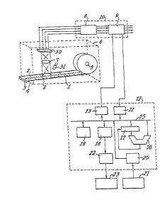
Figure l is a diagram of a tape rule having optical datacapture from encoder tracks and an associated data processing
system providing a digital position output;
Figure 2 shows a short length of the tape rule;
Figure 3 shows an analogue signal processing stage of the
data processing system;
~,~81~V~
Figure 4 is a diagram showing a sequence of allowed local
output states of the signal processing stage and transitions
between them within a signal sequence or block of tape absolute
position code (APC);
Figure 5 is a block diagram of a local state input and
decoder staye of a digital part of the data processing system;
Figure 6 is a block diagram oF a local state attribute
register and counter stage fed with output from the decoder stage
of Figure 5;
Figure 7 is a block diagram of decision logic operating on
the values of the attribute registers and counters of Figure 6 to
provide decoded APC bits to subsequent APC decoding logic;
Figure 8 shows state count logic providing a position output
within a current local state sequence that is available to a
microprocessor providing a control and output portion of the data
processing system;
Figure 9 shows APC decision logic that controls the handling
of APC data bits fed from the local state decoding logic of
Figures 5-~;
Figure 10 shows a pseudo-random number generator forming an
APC code generator stage of APC decoding logic; and
Figure 11 shows a sensed APC bit shift register and
comparator stage forming the remainder of the APC decoding logic.
THE SYSTEM OVERALL
In the drawings, there is shown a steel tape rule that
incorporates an electronic system that can give a digital reading
of length, measured in either metric of imperial units. In use
the tape operates in a similar manner to a conventional steel
~8~8~
rule but can include additlonal features to assist the user, for
example, automatic correction of reading for reveal measurement,
taking the tape body width into account.
The proposed measurement method is described below in
conjunction with Figure 1. A tape l of steel or other
inextensible material is used as in a conventional tape rule
controlled by a tensator spring S but is printed with a pair of
spatial encoded tracks 3, 4 in addition to the usual visually
readable distance scales 2. Internal to a casing 6 of the
product, the tape l is illuminated by means of a light-emitting
diode 31 and an image of the encoder tracks 3, 4 is formed using
a lens 7 on a photosensor array 30 which is arranged to have four
sensitive areas in grouped pairs corresponding to the paired
encoder tracks 3, 4. Each sensitive area views a small part of
its encoder track. The pairs of sensors in array 30 are aligned
with the tracks 3, 4 which are defined by mark and space or black
and white areas of varying widths, printed on the tape 1, and
imaged at the photosensors. Movement of the tape l causes the
light level at each photosensor 30a (Figure 4) to vary as the
area of the tape l corresponding to an individual photosensitive
area 30a changes between black and white. By suitable analogue
processing, four binary signals, one for each photosensitive area
30a, are derived from the photosensor outputs. The two states oE
the signals represent black or white at the areas on the tape l
corresponding to each of the photosensors. Movement of the tape
l causes the binary signals to change as the encoder tracks 3, 4
move past the photosensitive areas 30a.
~X ~ ~8~
The pattern of the encoder tracks 3, 4 and the spacing of
the photosensors 30a are arranged so that for every position on
the tape 1, incremental movements of the tape 1 cause only one of
the outputs to change state at a time. Sequences of states
fulfilling this criterion are known as Gray codes. Additionally,
it can be arranged that the direction of movement can, at all
times, be deduced from the change in output states.
As is apparent from Figure 1, the output of sensor array 30
is fed to an analogue processing circuit 8 and then to CMOS
digital processing logic 9 which are implemented in a single
application-specified integrated circuit (ASIC) 10 that provides
data at input port 11 of a 4-bit CMOS mask-programmed
microprocessor 12 and receives information and commands through
an output port 13. The digital processing logic 9 of the ASIC 10
includes a local state decoder and an APC binary sequence decoder
that are both implemented as logic and hence can run much more
rapidly than the microprocessor 12 so that the code tracks 3, 4
can be followed even during rapid tape movement. The
architecture of the microprocessor 12 is similar to a
conventional calculator-type microprocessor and the ports 11, 13
communicate via a 4-bit bus 15 with an ALU 16, accumulator 17,
display RAM 18 and general purpose RAM 19 which may be of 2~4 K
size. A keypad 21 communicates with the bus 15 through input
port 20 that may read up to 12 keys. The output value to be
displayed is fed from display RAM 18 to a display driver 22 that
may conveniently drive a display of up to 64 segments and is
shown on a liquid crystal display 23.
~'2~
ANALOGUE S I GNAL PROCE S S I NG
The two encoder tracks 3, 4 as explained above, are read by
four photosensors 30 that are illuminated either by a single
light-emitting diode 31 or by a pair of photodiodes 31 that
illuminate a region of the tracks. In Figure 3, only a 5ingle
photosensor 30 is shown, but the remaining three channels closely
resemble the channel illustrated. Each photosensor signal is
passed through a respective signal conditioner comprising an
amplifier 32, integrator 33 and comparator 34. The output of
integrator 33 is further fed to a 4-channel peak detector 35 and
the output of the channel having the highest signal level is fed
through attenuator 36 to a second input to comparator 34. The
arrangement is such that channels in which the signal level is
close to the peak level within the limit set b~ attenuator 36
will record logic 1 at 4-bit latch 37 and channels with a lesser
signal level will show a logic 0. The peak output of detector 35
is fed to a voltage controlled current source 38 that controls
the brightness of light-emitting diode 31. A timing and control
circuit 39 including an oscillator and latched gates provides
enabling pulses at line ~0 to the current source 38 to strobe the
light-emitting diode 31 and further provides a data ready pulse
at output line 41 ~o instruct subsequent logic that the output of
latch 37 may be read. The use of pulses rather than a continuous
output for light-emitting diode 31 reduces power consumption, and
the pulsing frequency selected will be sufficiently rapid (e.g.
40 KHz~ to allow the code tracks to be read under normal
conditions of use, as the tape is extended from and retracted
,`~
1~8~8~
into the housing. The peak detector 35 and attenuator 36
provides dynamic thresholding of the signal level at the input to
comparator 3~ so that a binary output representing mark or space
(black or white) areas of the tape is continuously available.
LOCAL STATE DECODING
Figure 4 shows a sequence of local states occurring in
blocks each defining one bit of the absolute position code (APC)
laid down along the tape and shows two alternative sequences by
which the photosensors 30a can change in state from 0011 to 1100
and bac~ again to 0011, the sequence reverting to its initial
value of 0011 at the 8th transition irrespective of which path is
taken. It is to be understood that the pattern of mark and space
markings defining the tracks 3, 4 will be laid down end to end
along the tape so as to implement the left hand or the right hand
sequence of Figure ~ with the initial 0011 state being common to
adjoining blocks. State changes are arranged to occur when the
tape 1 and photosensors 30 are moved relative to one another
through an interval of displacement and the pattern of marks and
spaces is computer-generated and laid down along the tape 1 to
implement the required sequence of local states as viewed by the
sensor array 30, changes between 0 and 1 of the four b.it pattern
commanding changes from dark to light of the maxkings viewed by
the respective sensors and the lengths of the individual dark and
light markings. It will be noted that the successive transitions
in each path conform to a Gray code in that each differs from its
neighbours by one bit only, and that each of the states has a
unique value, so that two successive states sensed by the
photosensor 30 give both the direction of tape movement and
~1
~.28~8'~
position in the block. Thus successive output states of 0100 and
llOO uniquely define position 3 in a forward movement along the
right hand path defining an APC bit ~ whereas a transition from
0110 to 0111 uniquely defines position 6 in a reverse tape
movement along the left hand path defining an APC 1 bit. Figure
2 shows a section of tape bearing markings coded according to the
above scheme. In Figure 2 there is shown a pattern of markings
on the tape l that will obey the sequence of Figure 4 when read
by an appropriately spaced and ordered sensor array. Each APC
bit gives rise to one mark in each track 3, 4, and the marks
occur in diago~ally related pair.s each roughly corresponding to
one APC ~it. The correspondence is not exact, however, because
neighbouring APC states are conjoined and the dark markings are
sometimes wholly within the span of a single APC bit and
sometimes extend across a boundary between adjoining APC bits so
that the marking is common to adjacent bits. Each marking in a
track 3 or 4 may be long (5 intervals of pitch), medium (4
intervals of pitch) or short (3 intervals of pitch) and the
intervals between adjacent markings may vary between 3 intervals
of pitch in the case of a pair o~ adjacent long markings and S
intervals of pitch in the case of a pair of short markings. Each
APC O state may be perceived by eye as a diagonal pair of medium
and short or short and short markings in tracks 3, 4, Each APC l
state may be perceived by the presence of a medium and long or by
a long and long pair of diagonal markings in the tracks 3, 4.
The markings are read~by a set of four photosensor sitting
symmetrically over the tracks 3, 4 with the sensors being read
clockwise or anti-clockwise and with the pair of sensors reading
each track occurring at three intervals of pitch. With this
12
~-~8~l8~
arrangement the successive output s-tates of the sensors as the
tape l mo~es may be caused to obey Figure 4, these properties
arising by proper cooperation between the sensor array and the
markings on the tape.
The outputs from termination and encoding logic in F'igures 7
and 8 are as follows:
(1) a "state count" indicating the number of state
transitions recorded within a current APC block;
(2) an "APC CLOCK" pulse indicating that a complete
sequence of local states has been traversed and a newly sensed
APC bit has been decoded;
(3) a direction line 101, Figure 7, indicating blt having a
logic l value if the tape is moving`forward and a logic 0 value
if it is moving backwards;
(4) an APC bit line 108, Figure 7 which can have the values
0, 1 or -1;
(5) an "APC Hlf" line 103, Figure 7, which is set (logic l)
if there is an equal probability that the APC bit being looked at
is a 1 or a 0; and
(6) a minor error flag is set if there have been any
erroneous transitions in a local state cycle.
The "state count" (l) is passed direct to the microprocessor
12 to indicate tape position within the currently sensed APC
block and the remaining outputs are passed to APC decisions logic
when the end of a block has been reached. So the local state
decoding logic has to determine when a block has terminated and
the attributes of the APC bit decoded in that block.
.. .
.
~ 28~V~
Each local state transition seen within a local state block
may be one of five types:
(1) invalid: i.e. any transition that does not occur in
Figure 4;
(2) APC bit 1, forward;
(3) APC bit 1, backward;
( 4 ) APC bit 0, forward;
( 5 ) APC bi t 0, forward.
Determination of the category into which a transition falls
involves comparison of the current state of the output latch 37
with its previous states. In Figure 5 a first clock phase ~ and
data ready line 41 are inputs to AND gate 56 whose output when
high clocks current state register 54 so that when the data ready
line 41 i5 active the outputs Qo-Q3 oi the latch 37 are clocked
by clock phase 01 into the register 54. The previous state of
register 54 is clocked by the output of AND gate 56 into a last
state register 55. At the same time, the values in registers 54,
55 are clocked into decoding logic 57 that implements the local
state transition diagram of Figure 4 and derives therefrom a
decoded APC bit O or 1 according to whether the states in
registers 54, 55 lie on the left-or-right hand side of the
diagram of Figure 4, that APC bit appearing at line 50 as a logic
O or 1 output. Output line 51 provides an output bit significant
of current tape direction (forward or backward), output lines 52
provide a current position index within the APC block and output
line 53 provides an invalidity flag. Although gate 56 is cloc~ed
at each phase ~1, the latch 58 does not change the output state
14
~8~l8~
at lines 50-53 unless comparator 59 indicates that the contents
of registers 54, 55 are different, corresponding to tape movement
between one local state and the next and enables the clock phase
~1 to pass via AND gate 59a input to the clock input to latch 58.
Referring to Figure 6, logic is shown that operates
principally in clock phases ~2 and 03. Lines 51-53 communicate
with a current attribute register 70 that is clocked at phase 03.
sut in the previous phase ~2 the existing contents of register 70
are clocked into previous local position register 60 and previous
direction register 61 provided that a second input to AND gate 71
from attribute register 70 indicates that a valid transition had
been flagged in line 53. Clock phase ~2 also enables AND gate 89
to store previous consecutive valid transitions in register 81 as
will be more fully described below. On clock phase ~3, a number
of counters 75-80 are incremented or decremented either directly
in the case of transition counter 75 or via gates 82-87 in the
case of counters 76-80. Counter 76 is gated from lines Sl and 53
via gate 82 and records total valid forward transitions. Counter
77 is clocked through gate 83 from line 53 and line 51 with input
inversion and records total valid backwards transitions. Counter
78 is gated via gate 84 ~rom line 50, 53 and records total valid
transitions within an expected APC 1 bit: similarly counter 79 is
gated via gate 85 from line 53 and from line 50 with input
inversion and records total valid transitions within an expected
APC 0 bit. Counter 80 records consecutive valid transitions
within a given APC bit for a given direction. If the previous
direction continues on the next recognised APC bit exclusive OR
gate 88 is enabled, clocked flip/flop 94 that provides an
increment or decrement input to counter 80 remains at its
:, :
18~
previous (high) state and a valid transition at the input to gate
87 enables clock phase ~3 to pass to encounter 80 thereby
incrementing the number of valid counts. On direction change,
exclusive OR gate 88 toggles flip/flop 94 and the contents of
counter 80 are now decremented at each clock phase ~3. If an
invalid count is flagged at line 53 or reset line 90 is
activated, OR gate 93 resets the counter 80. A previous
consecutive valid tra~sitions register 81 is loaded from counter
80 to phase ~2 via AND gate 89 as mentioned above provided that
the current bit in line 53 is invalid and the output of counter
80 is not 0, control being via EXCLUSIVE OR gate 95. In clock
phase ~4 if the total forwards value in counter 76 equals the
total backwards value in counter 77, exclusive OR gate 99 gives a
low output to an inverting input of AND gate 91 which is fed via
OR gate 92 to reset line 90, thereby resetting all the counters
and registers 75-81 to their initial state. Resetting via OR
gate 92 also takes place whe~ system reset line 96 or encoding
logi~ reset line 97 are active.
In Figure 7 termination and encoding logic is applied to the
contents of the counters 75-81 to determine when the end of a
local state sequence has occurred and to provide an output for
subsequent processing. The values in counters 76, 77 provide
inputs to comparator 100 whose output at line 101 indicates tape
forward movement (logic l) or backwards movement (logic 0). The
total valid APC l count and total valid APC 0 count in registers
78, 79 are fed to comparator 102 which will give a logic 0 output
except when the contents are equal; the output of comparator 102
is at line 103. If the output in line 103 is logic 0 the
probability is that more than half of a local state cycle (APC
16
8~
bit) will have been decoded correctly, and this is recognised in
subsequent logic. If the contents in APC 0 register 7~ are zero
as detected by a comparator 104 and the contents of registers 78,
79 are equal as determined by comparator 102, an output from
comparator 104 and the output in line 103 enable AND gate 105 to
indicate a major error at li~e 106. An error flag in line 106
will be passed direct to the microprocessor 12 and will cause an
error indication to be given on the display 12. The contents of
registers 78, 79 are fed to comparator 107 whose output in line
108 indicates whether the APC bit being sensed is logic 1 or
logic 0.
Data in lines 101, 103, 106, 108 is ~ed to output latch 109,
and the remainder of the logic of Figure 7 is used to regulate
whether that output should be made available for subse~uent
processing. According to a first rule, i~ the current state is
equal to the start state of a local state se~uence and the
consecutive valid transitions are greater than or equal to a
threshold, then the output in latch 109 will be passed on.
Accordingly, the current state in register 54 is fed to one input
of comparator 110 whose other input i9 ` fed with a value e~ual to
the start value of the local state sequence (in this instance
0011). The output of comparator 110 is fed to one input of AND
gate 111 whose other output is fed with the contents of
consecutive transitions counter 80 through threshold comparator
112. If both inputs to gate 111 are high, a logic 1 output is
fed to OR gate 113 that in turn enables AND gate 114 to clock the
latch 109 at the next clock phase 05 thereby latching the state
17
~8~18~
count outputs into latch or buffer 109. According to a second
rule, the output latch 109 will be clocked on ~5 via O~ gate 113
and AND gate 114 if the following four conditions apply:
(a) the contents of previous consecutive valid transitions
counter 81 exceed a threshold set by compara'cor 115;
(b) the valid line 53 is set;
(c) the current direction is the same as the previous valid
direction as indicated at input line 116 from comparator 88; and
(d~ the current index in line 52 is less than a previous
valid index held in register 60 as determined by comparator 118.
When the above four conditions are satisfied the output at
gate 117 goes to logic 1. The object o~ this rule is to take
account of sensing errors at the boundaries o~ state blocks
resulting in failure to recognise that the last block has ended
and a new block is being sensed.
According to a third rule, if the current index equals the
previously valid index and equals zero (indicating no tape
movement) and the number o~ transitions represents adjacency to
the end of a cycle (7 transitions in this instance) then gates
113, 114 clock the output latch 109. Accordingly the ~ollowing
conditions must apply:
(a) the value in transition count register 75 fed through
threshold (>7) detector 119 provides an enabling input to AND
gate 120; and
(b) the contents o~ previously valid index register 60 and
current index in line 52 are both equal to 0 as determined by
comparator 121 giving an enabling input to AND gate 120.
1~
~'2.~
The effect of the third rule is to bring about a transition
independent of an error at the end of a block.
Figures 8 shows state count logic that identifies the
position of the counters within the currently read APC state
sequence based on a previously valid index in position register
60 and a previously valid direction in direction register 61. An
accumulator 62 is clocked at clock phase 03 to load the value o~
previously valid index from registers 60 and on clock phase 0~
the value in accumulator 62 is incremented by 1. On clock phase
05 the new value in accumulator 62 is loaded into latch 63 as a
state count output available to the microprocessor 12 together,
with tape direction from register 61.` Accordingly a current tape
position within the local state sequence being read is available
to the microprocessor 12 to give fine positioning of the tape 1.
It follows therefore that the local state decoding stage of
the digital processing logic 9 supplies a local state count
output for direct processing by the microprocessor 12 together
with an APC bit, tape direction and error fla~ information to
subsequent APC decoding logic ~orming part of the digital
processing logic 9.
THE APC-DECODING LOGIC
The APC decoding logic of Figures ~-11 receives APC bit
information from the local encoding logic of Figures 5-8, and
assembles successive APC bit into an n-bit APC word which in the
present instance is eleven bits long and is stored in a shift
register n-bits long clocked on detection o~ each APC bit. It
contains an APC code generator that when clocked from an initial
state reproduces the sequence o~ APC bits laid down on the tape,
~9
~ 8~
a comparator for determining a match of t:he state of the APC code
generator with that of the sensed APC word shift register, and a
counter for indicating how many register clock pulses are
required to achie~e a match, the value in the counter being
significant of position in the APC sequence and hence of tape
posltlon .
Means are provided for initialisation and rapid clocking of
the code generator until a match is obtained, followed by
clocking on successive incoming APC bit~ so that the bit pattern
in the APC word shift register is tracked by the state of the APC
code generator. Error checking is provided by a "look ahead"
facility in which an incoming APC bit is compared with an
expected APC bit from the APC code generator and an error is
flaaged if a match is not obtained.
The circuit of Figure 9 controls the processing of APC data
fed via latch 109 and toggles between a normal mode in which a
clock pulse is generated on a pseudo-random bit generator (PRBG)
clock line on every ~PC bit, and a reset mode in which sequential
APC bits are counted to enable tape position to be recalculated.
In an error condition, OR gate 130 receives an input from APC
half-bit output line 103 through latch 109 or an invalid APC bit
from line 129 (Figure 11) indicating either that the local ~state
logic has been unable to decode a local state sequence or that
the APC bit from the local state logic is not the expected next
bit in the APC sequence.
In either of these events, output of OR gate 130 goes high
and is clocked on the next system clock through latch 131 to a
re~et line 132. The line 132 also goes high i~ a reset signal is
l'~B~L~I 8~
received from the microprocessor 12 via line 133 and output port
13. The state of reset line 132 is fed through OR gate 134 to
reset an n-bit counter 135. The error signaled ~t line 132
cloc~s latch 136 to cause a bad APC line 137 to go low and the
state on line 137 is also fed to one input of a direction match
OR gate 138 whose other input from line 101 is at logic 1 when
the tape is going forward, the direction output from gate 138
being at line 139.
The value on line 101 is also fed into latch 140 the
contents of which are put out at line 141 when an APC clock
signal of phase ~3 occurs in line 142. The forward direction at
line 101 and last forward direction at line 141 are compared at
EXCLUSIVE OR gate 143 and if different cause direction change
line 144 to be set. The direction change signal at line 144 is
also inverted and fed to AND gate 145 whose other input is the
APC clock phase ~3 and whose output goes to the clock input of
counter 135. The direction of count is governed by the value in
llnes 101, 146 so that when the signal at line 146 is high, the
counter 135 counts in a positive sense and when the signal is
low, counts in a negative sense. The shlft register counter 135
has outputs >11 or <-11 (depending upon the state of line 146),
which form inputs to OR gate 147 which clocks latch 149 via line
148. The input to latch 149 is a constant logic 1. The input to
latch 136 is a constant logic 0. Latches 136, 149 are enabled
via line 150 which is an output of AND gate 151. The inputs to
AND gate 151 are a comparator input 152 (Fig. 11~ and a "get
match" output 153 from latch 149. Assuming that the value in the
PRBG shift register 164 is not the same as the value in the APC
21
'
~ 8~
shift register 184, then comparator line 152 will be high, the
"get match" line 153 will also be set high and line 150 will
further be high, enabling latches 149, 136. The outputs of
latches 149, 136 are fed as inverting and normal inputs to gate
154 fed with system clock pulses at 155 which appear at output
line 156 as an input to OR gate 157. Accordingly, in an error
condition the system clock equals the pseudo-random-bit generator
(PRBG) clock 158, In a non-error state line 137 is set to logic
1 which enables the APC clock phase T3 at line 142 to be passed
through AND gate 159, output line 160, and OR gate 157 so that
the APC clock at line 142 provides the PRBG clock 158.
Accordingly the decision logic toggles the output at line 158
between an error state in which fast system clack pulses from
line 155 appear and a normal mode in which a clock pulse appears
when an APC bit has been decoded as indicated by a pulse in line
142.
Figure 10 shows a pseudo-random bit or number generator for
generating within the digital processing circuitry a sequence of
pseudo-random numbers corresponding to the APC bit sequence on
the tape. It may be controlled according to the direction of
movement of the tape to generate the APC bit which is above or
below the current APC position and generates an APC count
corresponding to the position of the APC sequence in the pseudo-
random number sequence. PRBG cloclc pulses at line 158 are
connected to APC up/down counter 161 which counts in a sense
toggled by direction line 101. The clock line 158 and direction
change line 144 are input into gate 162 whose output in line 163
provides a clock into an n-bit shift register 164 whose direction
'~ j ~
22
,
~ 8~
of clocking is set by direction line 101 and that can be reset
via line 132 (Fig. 9). The shift register has inputs 169, 170
and taps are taken at intermediate positions 165-168. Taps 165,
167 form an input to EXCLUSIVE OR gate 171 whose output provides
input 169 to shift register 164. Taps 166, 168 form an input to
EXCLUSIVE OR gate 172 whose output pro~ides input 170 to the
shift register 164. This combination of taps and gates is
selected to generate an appropriate pseudo-random sequence. Taps
166, 170 form an input to selector 173 whose output 174 depends
on the state of the match direction value in line 139. Thus in
normal operation line 139 changes state between forwards and
reverse tape travel, but under error conditions the line 139 is
held to logic 0 so that the selectors 173, 176 are set to look at
taps of the shift register 164 corresponding to forward movement.
Similarly taps 169, 175 from the shift register form an input to
selector 176 whose output 177 depends upon the match direction
value in line 139. The bits in output lines 174, 177 from
selectors 173, 176 are the expected next forward and reverse bits
in the APC sequence. Thus the register 164 acts as a decoder for
the APC code on the tape 1 (that will have been generated by a
similar clocked shift register acting as an encoder) and provides
a "look ahead" facility.
Figure 11 shows how detected APC bits are gathered for
comparison. The expected APC bits at 174, 177 are fed to
selector 182 controlled by the signal in line 101 and one of them
is passed as an output in line 181. The forward bit (bit f) in
line 174 is output if line 101 is high, otherwise the backwards
bit ~bit b) in line 177 is output. The expected APC bit in line
~ 8'~
181 forms one input to selector 180 whose other input bit is the
decoded APC bit at line 108. Selector 180 is controlled by bad
APC signal line 137 to pass the expected bit 181 to line 183
under normal conditions, thereby allowing a decoded APC shift
register 184 to ignore errors in decodi.ng single APC bits, or the
decoded bit in line 108 during the reset condition when
accumulating a new APC code. The detected or substituted APC
code bits at 183 are fed successively into and through the n-bit
shift register 184 which accumulates an APC word consisting of
the last n decoded or substituted APC bits (in this instance
n=11). EXCLUSIVE OR gate 185 compares the expected APC bit at
181 with the decoded bit at 108. If they are both the same,
output 186 of gate 185 stays low but if they are different then
output 186 of gate 185 goes high. In the absence of an APC hlf
signal the signal in line 103 which forms an inverting input to
AND gate 187 is low. The nput to gate 187 from line 186 will
remain low while there is a match between the expected and
decoded APC bits and the outp~t 188 of the gate 187 will remain
low: otherwise line 186 and 188 go high indicating a mismatch in
the expected and encoded APC bits. If the APC half line 103 is
high indicating uncertainty in the APC bit from the local state
decoding the line 188 will remain low irrespective of the state
of line 186. A mismatch in decoded and expected APC bits
detected at gate 18S will set a latch 202 (described below) to
indicate a l-bit error and will start clocking of an error
counter 207.
2A
~8~a~
An inverted direction change signal at direction change line
144 and APC CLK signals of phase T2 in line 192 form inputs to
AND gate 191 so that APC clock pulses are passed to line 190 when
line 144 is set low. When direction change input line 144 is low
the APC CLK signals of phase T2 appears on clock input 195 of
shift register 184. The signals on line 188, 190 are combined at
AND gate 189 whose output line 201 will also carry an APC CLK
signal of phase T2 provided that (i) the APC hlf line 103 remains
low, (ii) the direction change line 144 remains low and (iii) the
lines 186 and 188 have gone high, indicating that the expected
and decoded APC bits difer.
APC CLK pulses of phase T2 in output line 201 of AND gate
189 appears as a clock input to latch 202 and an input to AND
gate 203~ The effect of the APC CLK pulses in line 201 is (a) to
set the output 220 oE latch 202 that has a logic 1 input high
when line 201 goes high, and (b) where AND gate 203 is enabled
through line 22~ to pass to the invalid APC line 129~
When a first erroneous APC bit is detected, an error counter
207 is cleared and set to count through a set of the next n APC
bits so that track is kept of the substituted APC bit in relation
to the sequence being built up in the shift register 184. ~hen
there has been no tape direction change and the direction change
line 144 that provides an inverting input to AND gate 216 is low,
the gate 216 passes APC CLK pulses o phase Tl carried by line
217, and the clock pulses are carried by output line 215 to AND
gate 213. Output 212 of AND gate 213 carries a clock when input
215 to gate 213 carries a clock when input 215 to gate 213
carries the APC CLK pulses of phase Tl.
.
8~
Input 214 of AND gate 213 will have been latched high by
latch 202 signifying an APC bit in error. If a decoded APC bit
is or was in error and -the consequent substituted APC bit is one
of the n APC bits present in shift register 184, the error
counter 207 will be clocked by the APC CLK pulses of phase Tl as
every decoded APC bit i.s generated. If the tape direction input
at line 101 to count~r 207 is low then the count in counter 207
is decremented for every clock pulse, but if line 101 is high,
then the count at counter 207 is incremented. If the count in
counter 207 reaches n or -n, then output 230 or output 231 are
set high, these lines providing inputs to OR gate 210. When
either of lines 230 or 231 goes high, the output line 211 of OR
gate 210 is also set high, that line providing a logic 1 input to
OR gate 204 so that the output line 218 goes high and resets the
error counter 207 to zero through OR gate 204 that also passes a
reset signal on line 132. Therefore if a decoded APC bit did not
match the expected value in either forward or reverse tape
travel, the expected APC bit has been fed into shift ragister 184
in substitution ~or the erroneously decoded bit, and by
subsequent tape movement the substituted bit has been clocked out
of the shift register 184 by n consecutive clock pulses then the
error counter 207 is reset to zero. The high value of line 211
is also input to OR gate 221 whose output line goes high and
resets latch 202. (The other input to OR gate 221 is via reset
line 132.) The consequent low output in line 220 from latch 20?
is input via line 214 to AND gate 213 which now will not transmit
APC CLK pulses of phase Tl to counter 207. AND gate 203 is also
disabled because its input at line 220 is low, and ~PC CLK pulses
of phase T2 can no longer pass to line 129. Consequently an
. ..
26
.
erroneous decoded APC bit can be substituted with an expected APC
bit and the n-bit APC code in shift register 184 will be
preserved provided that the next n decoded APC bits match their
expected values. No output will appear at the invalid APC line
129 on a first invalid APC bit because output 220 of latch 202
will be low during the relevant APC clock pulse of phase T2. But
the circuit of Figure 11 responds to a second erroneous APC bit
within a word of n APC bits by outputting an invalid APC flag at
line 129 which forces the system to reset. If a previous error
has been detected and the substituted APC bit is still in shift
register 184, the output line 220 of latch 202 is set high and
enables AND gate 20~. If a second error occurs, input line 201
to AND gate 203 goes high again, setting the invalid APC output
line 129 high and forcing the system into reset. In this way the
circuit of Figure 11 can recover from a single APC bit error in
an n-bit sequence but will reset if a second error has occurred
in the same sequence, causing a reset in the decision logic of
Figure 9.
Assuming no direction change at 144, inccming APC CLK pulses
of phase T2 at line 192 pass via AND gate 191 and line 190 to the
clock input 195 of the shift register 184 whose n-APC sensed bit
output at lines 196 forms one input to comparator 197 whose other
input 200 is the current value of the generated APC code in shift
register 164. The output line 152 from comparator 157 is low
when the generated APC code in decoder or PRBG shift register 164
matches the sequence of sensed and decoded APC bits in register
184 and provides an input to gate 151 that toggles the clock
pulses at line 158 between system clocking from line 155 and APC
clocking from line 142. Thereby the APC decoding shift register
Z7
'
164 is clocked rapidly by system clock pulses until a match is
obtained and thereafter, provided that the match at comparator
197 is maintained changes state only with incoming APC bits.
Assuming that valid transitions have been sensed at both the
local state and APC levels, the state count output in latch 63
and the value in APC counter 161 are available through input port
11 to the microprocessor 12 where they are combined by a position
analysis program to derive the position o~ the tape 1 relative to
the casing 6, which position is output through display RA~ 18 to
the liquid crystal display 23.
b:SD1:5361-l.spe/Jan.09.90¦sm
~8