Note: Descriptions are shown in the official language in which they were submitted.
1~3Z~L7 `-
- 1 - 45MR 508
ADAPTIVE LIMITER/DETECTOR WHICH CHANGES
TIME CONSTANT UPON DETECTION
OF DOTTING PATTERN
FIELD OF THE INVENTION
The present invention relates to digital
radio communications receivers, and more particularly,
to detection and decoding of digital
signals transmitted over a slotted radio frequency
communications control channel of a digitally trunked
communications system.
BRIEF DESCRIPTION OF THE DRAWINGS
These and other features and advantages of
the present invention will be better and more
completely understood by reading the following
detailed description in conjunction with the appended
sheets of drawings, of which:
FIGURE lA is a graphical illustration of an
incoming digital data signal detected using a
non-adapting threshold level;
FIGURE lB is a graphical illustration of an
incoming digital data signal detected using an
adapting threshold level;
FIGURE 2 is a schematic diagram of a prior
art adaptive limiter circuit;
.
i~
.
- 2 - 45MR 508
FIGURE 3 is a schematic diagram of control
and work channel signalling in an exemplary digitally
trunked communications system;
FIGURE ~ is a schematic diagram of exemplary
signalllng formats of the messages shown in FIGURE 3;
FIGURE 5 is a schematic diagram of the
presently preferred exemplary embodiment adaptive
limiter circuit in accordance with the present
invention;
FIGURE 6 is a flow chart of exemplary
program control steps performed by the circuitry shown
in FIGURE 5; and
FIGURE 7 is a graphical illustration showing
the response of the prior art FIGURE 2 limiter circuit
to receipt of an input signal and the response of the
preferred embodiment circuit shown in FIGURE 5 to
receipt of the same input signal.
BAC~GROUND AND SU~MARY OF THE INVENTION
It is now common for digital signals to be
transmitted over radio frequency communications
channels. Received demodulated digital signals
typically have AC and DC components -- that is, the
incoming digital bit stream is typically superimposed
upon a DC level the amplitude of which depends upon
several factors (e.g., the difference between the
transmitter RF carrier frequency and the receiver RF
tuning frequency, and the biasing of the receiver
radio frequency circuitry). This DC component can
vary greatly in dependence on these factors.
It usually takes on the order of 10-20
milliseconds or so for a receiver to "lock on" to the
transmit carrier frequency (e.g., by operation of a
trackin~ feedback-controlled phase locked loop local
oscillator as is well known). The level of the DC
component upon which the incoming digital data stream
~ 28~ 7
- 3 - 45MR 508
is superimposed is typically directly proportional to
the difference between the transmitter carrier
frequency and the frequency to which the receiver is
tuned. This DC level commonly exhibits a transient
maximum upon (or shortly after) initial receip-t of an
RF carrier by the receiver (and duriny the time the
receiver local oscillator attempts to synchronize with
the transmitter carrier frequency) before
"stabilizing" to a steady state level.
To detect the digital data stream
superimposed upon a DC component, digital radio
receivers generally include a limiter circuit which
distinguishes between the DC component and the digital
signal stream superimposed upon the DC component --
and produces an output responsive only to the digital
signal stream. A simple such limiter circuit compares
the received signal with a predetermined fixed
threshold level. Any time the signal level is above
the threshold level, the limiter produces a logic
level 1 output -- and the limiter produces a logic
level 0 output whenever the level of the received
signal is below the threshold level.
Since the DC level of the received signal
varies with the difference hetween the incoming
carrier frequency and the receiver tuning frequency,
DC biases within the radio circuitry, and other
factors, use of a fixed limiter threshold leads to
signal detection errors. An improved prior art
limiter averages the incoming signal in order to track
changes in the receiver DC bias -- and uses the signal
average as the threshold level. Such averaging
limiters are called "adaptive" because they adapt to
changes in the incoming signal DC component.
FIGURE lA is a graphical illustration of a
received digital signal waveform 10 relative to a
. . . . .
.: ,'. - . :
,
~2~2~7
- 4 - ~5MR 508
non-adapting (i.e., fixed) DC threshold level 12. As
mentioned previously, digital signal stream 10 is
superimposed upon a DC level which changes with time.
At a time to, threshold level 12 can be use~ by a
signal comparator to distinguish between digital
signal logic level 0 and logic level 1 because i-t
falls about midway between those two logic levels. As
the receiver local oscillator frequency changes with
respect to the transmitter carrier frequency (and/or
receiver bias shift occurs), however, the DC level
upon which the digital signal is superimposed shifts,
causing both the digital signal logic level 0 and the
digital signal logic level 1 to shift relative to
fixed threshold level 12. By time t1 in the example
the fixed threshold level 12 is about the same as
digital signal logic level 1 and can no longer be used
to differential between logic level 0 and logic level
1. As FIGURE lA demonstrates, soon after the DC
component of the incoming signal shifts, a
non-adapting limiter begins detecting only logic
level zeros or logic level ones.
FIGURE 2 is a schematic diagram of a prior
art adapting limiter circuit 20. In this circuit,
comparator 22 is used to compare the instantaneous
value of the incoming signal Vin with an integrated
(averaged) version of the incoming signal (signal
level averaging being performed by RC network 24).
More particularly, a first resistor 26 connects Vin
to the non-inverting input of comparator 22, and a
resistor 28 connects Vin to the inverting input of
the comparator. A capacitor 30 connected between the
comparator inverting input and ground (reference)
potential stores charge and resists changes in the
voltage level present at the comparator inverting
input. ~he voltage Vc present across capacitor 30
''
- , ,
~Z82~1 7
- 5 - 45MR 508
can be used as an adapting threshold level 12, since
it has a value approximately equal to the average DC
level of the incoming signal Vin over a short time
period the duration of which depends on the time
constant of RC network 24 (and is therefore about
midway between signal logic level 1 and loyic level
O) .
When the signal level at the comparator
non-inverting input exceeds the signal level at the
comparator inverting input, comparator 22 detects a
logic level 1 and applies the logic level 1 output
signal to the input of modem 32. When the signal
level at the comparator non-inverting input is less
than the DC level stored by capacitor 30, comparator
22 detects a logic level 0 and applies a logic level 0
signal level to the input of modem 32.
Modem 32 groups the incoming serial digital
data bits into parallel bit units (e.g., bytes)
convenient for processing by microprocessor 34 and
communicates these signal units to the microprocessor
for analysis. The microprocessor may detect and/or
decode the incoming digital signal in a conventional
manner.
FIGURE lB is a graphical illustration of the
same incoming digital signal 20 shown in FIGURE lA
relative to an adapting threshold level 12 produced by
RC network 24 of the FIGURE 2 adapting limiter
circuit. Because threshold level 12 adapts to the
changing DC component of the incoming signal, the
limiter successfully distinguishes between digital
signal logic level 1 and digital logic level 0 despite
changes in the DC component due to receiver bias,
receiver tuning, and other effects.
Resistor 28 and capacitor 30 values must be
selected appropriately to allow circuit 20 to adapt
- 6 - 45MR 508
quickly enough to the changing DC component without
adapting too rapidly. The time constant of RC network
24 should be sufficiently fast to adapt to drift in
the incoming signal DC component. But because a long
string of logic level ls or logic level Os changes the
average DC level of the incoming signal over the
duration of the string, the time constant of RC
network 24 cannot be too fast or else circuit 20
begins to detect bits improperly because it "adapts"
lo to the content of the incoming digital signal rather
than only to the more slowly changing DC component on
which the incoming signal is superimposed.
Further complications arise if the incoming
digital signal includes significant low frequency
components. For example, General Electric's Public
Service Trunking Communications System transmits and
receives digital data signals having significant
frequency components as low as 10 Hz (e.g., subauclible
digital signalling used to confirm proper channel
allocation and/or to direct units to other channels in
order to receive a higher priority call). The
averaging process performed by RC network 24 is the
equivalent of high-pass filtering in the frequency
domain -- and the network must pass frequencies as low
as 10 Hz if modem 32 is to receive the intelligence
carried by the low frequency components. The RC
network must have a very slow time constant if the
threshold level is not to "adapt" to the lower
frequency components of the incoming digital signal.
It is highly desirable for the receiver to
begin reliably detecting the incoming digital signal
as soon as possible after initial carrier signal
receipt. With an RC time constant which is long
enough to prevent limiter circuit 20 from adapting to
a 10 Hz bit rate, the circuit takes a long time to
,- . ~ ' ' -
~28~
- 7 - 45MR 508
adapt to shifts in the varylng DC component the
incoming digital signal is superimposed upon. As a
result, the receiver may take 20-30 milliseconds or
more to adapt after first receipt of the carrier
signal.
One possible solution to this problem is
discussed in U.S. Patent No. 4,631,737 to Davis et al
(1986). This patent discloses a limiter circuit which
detects the "peaks" (maxima) and "valleys" (minima) of
lo the incoming signal~ Davis et al's limiter sets a
limiter threshold level to the midpoint between the
average maximum signal level and the average minimum
signal level. This is a general solution to the DC
drift/offset problem, and also functions effectively
for any type of signal (e.g., incoming digital signal
sequences having more logic level 1 bits than logic
level O bits or vice versa)~
One disadvantage to this approach is that is
relatively complex -- requiring minima and maxima
signal level detection circuitry.
Davis et al discuss (at Column 3, lines
27-64; see also FIGURE 2) a data limiter circuit
within an RF receiver some circuitry of which is
powered off during periods of in inactivity in order
to save battery power. The limiter includes a
transistor which functions as a switch to change the
time constant of a coupling network between the
receiver and the limiter -- allowing proper bias
voltage level to be established on the coupling
capacitor during initial receipt of a signal between
the receiver has been fully activated. The transistor
alters the RC time constant to a value needed for
proper operation of the limiter when a battery saver
circuit restores interrupted power to the receiver
circuitry. Davis et al observe that this circuit
3Z9~7
- 8 - 45MR 508
suffers from the disadvantage that for FSK binary
signalling the received bit stream must have nearly a
fifty percent dut~ cycle of ls and Os during the time
the capacitor is being rapidly charyed (for otherwise
the resultant bias voltage established on the
capacitor is not the appropriate level needed for
correct operation of the limiter).
Another approach is disclosed in U.S. Patent
No. 4,575,863 to sutcher et al (1986). Butcher's fast
recovery bias circuit includes a limiter circuit which
adaptively alters the receiver limiter operating bias
level based on detection of a work synchronization bit
pattern. The combination of resistors 24 and 26 (see
FIGURE 2) forms a low-pass filter with a corner
frequency of about 50 Hz when a switch 40 is
activated. Capacitor 32 rapidly charges to the
average voltage`of the received data signal.
Comparator 34 processes the received data signal to
provide binary 1-0 information to the data decoder 20.
If a word sync binary pattern is detected by
the Butcher data decoder 20, switch 40 is deactivated
-- reducing the corner frequency of the input circuit
to approximately 5 Hz. The increased time constant
(that is, reduced corner frequency) prevents reference
25 voltage shifts which could normally occur due to long
strings of ones and zeros in a binary signal pattern.
When an end of message condition is detected by
decoder 20, switch 40 is once again activated to
decrease the input circuit time constant.
The Butcher et al limiter arrangement
provides increased limiter adaptivity rate at the
beginning of a received message. However, Further
improvements are possible.
In General Electric's new "Public Service
Trunking" communication protocol (see
,: ' ' - ' ~, ' ~' .;. ' ' '
~32~
- 9 - 45MR 508
commonly-assigned Canadian Application Serial ~Jo. 566,664
of Childress et al, filed ~lay 12, 1988,
entitled "Trunked Radio Repeater System"), a "slotted"
dedicated control channel is used to pass digital
channel allocation request signals from mobile
transceivers ac~uiring service to the site
controller. In an exemplary embodiment described in
that Canadian application, the control channel is
fully duplexed so that there may be simultaneous
"in-bound" and "out-bound" control channel
signalling. The system is "digitally" trunked in that
trunking control is effected by digital signals passed
over the continuously dedicated time division
multiplexed "control" data channel.
FIGURE 3 schematically shows calling
protocol for in-bound and out-bound frequencies of the
dedicated control channel in GE's Public Service
Trunking System. A mobile transceiver desiring to
communicate via a repeater transmits a channel request
message on the control channel in-bound frequency --
this channel request message having a total duration
(including time for transmitting bit and word
synchronization fields and error checking fields) of
only 30 milliseconds. The repeater receives, decodes
and processes the channel request message, and within
60 milliseconds after the last part of the channel
request message has been received, transmits a
responsive channel assignment message on the outbound
control channel (this assignment message specifying a
working channel frequency as well as other
information). The mobile transceiver receives the
channel assignment message and changes frequency to
the working channel specified by the channel
assignment message -- the entire channel
request/allocation process being completed within 280
~L2~ 7
- 10 - ~5MR 508
milliseconds after the time the calliny mobile
transceiver began transmitting the channel request
message.
FIGURE 4 is a schematic diagram of
exemplary formats for -the messages shown in FIGURE 3.
Reference numeral 80 refers to the outgoing recurriny
signals transmitted by the repeater on the out-bound
control channel frequency, while reference numeral 82
refers to the channel request message transmitted by
the mobile transceiver on the in-bound control channel
frequency.
In the preferred embodiment, the channel
request message is preceded by 152 bits of dotting
pattern (i.e., a string of alternating binary valued
bits -- 101010). Following the dotting pattern, three
repetitions of a word ("frame") synchronization code
(a 16 bit Barker code in the preferred embodiment) are
transmitted, after which is transmitted a 40 bit
message specifying the type of communications required
and an identification of the calling and called mobile
units ~in the preferred embodiment, the message
portion is transmitted three times, once inverted, to
increase the probability of correct reception).
In the preferred embodiment, all signalling
occurs at 9600 baud in order to improve system
response time. One of the design objectives set forth
in the "APC0-16 Requirements" (published by the
Association of Police Communications Officers) is that
any user must have voice channel access within
one-half second after engaging a push-to-talk (PTT)
switch. The exemplary embodiment utilizes the highest
possible data rate (e.g., 9600 bps on the typical
25 KHz bandwidth radio channel) for critical control
channel signalling in order to ensure very rapid voice
channel access. The 320 bit-long channel request
-' ,, . :
-
.
.
329l~7
~ 5MR 508
message transmitted on the in-bound control channel
frequency by the mobile unit is transmitted at 9600
baud in only 33 milliseconds or so -- and the initial
152 bit dottiny portion of the channel request message
has a duration of only about 16 milliseconds.
It will be appreciated by those skilled in
the art that when such short message durations are
involved, it is especially critical for receivers
(e.g., the repeater receiver) to very rapidly being
properly detecting incoming signal levels. For
- example, the repeater receiver limiter must begin
properly and reliably decoding the incoming signal by
the time the Barker code portion of the channel
request message is received if proper frame
synchronization is to be ac~uired.
The limiter disclosed in the Butcher et al
patent operates at a high adaptivity rate (time
constant = 20 milliseconds) until word sync (e.g.,
Barker code) has been received and successfully
decoded. Decoding word sync, however, takes a
substantial amount of time (a typical word
synchronization bit pattern is lO or more bits long).
Moreover, the receiver must acquire bit
synchronization before it can properly decode the word
synchronization bit pattern. Significant problems
result from waiting until after the word
synchronization code has been properly detected before
increasing the limiter adaptivity time constant.
Transmission of dotting pattern permits a
receiver to very rapidly acquire bit synchronization.
In fact, no other bit pattern allows a receiver to
synchronize with the incoming bit timing as rapidly
and efficiently. In addition, dotting pattern can be
decoded very rapidly and successfully because it is a
simple, alternating binary valued bit pattern -- and
:
.- . :
. .
.. ' ,
- .:
- 12 - 45MR 508
an arbitrary desired number of received dotting
pattern bits can be tested to determine whether the
dotting pattern has been received.
It is therefore highly advantageous for
every message to be preceded by a dottlny pattern
(see, e.g., commonly-assigned U.S. Patent No.
4,663,765 issuing to Sutphin on May 5, ~987,
discloslng a communications receiver which unmutes
audio output in response to proper detection of a
dotting pattern preamble).
Another important design goal is
conservation of the processing capabllitles of the
receiver microprocessor used to decode and process
incoming signals. When incoming signalling is
received, the digital signal processor associated with
the control channel typically must cease performing
other tasks and begin processing the incoming
signals. If the processor determines that the
incoming signalling is intended for it and must be
decoded, it typically must devote substantially all of
its processing cycles to decoding and other~ise
processing the incoming signalling. On the other
hand, if the processor determines that the incoming
signalling need not be decoded (e.g., the signalling
may not match a predetermined protocol and therefore
can be ignored), the processor can perform other
useful tasks (e.g., maintenance functions) instead.
It is therefore desirable for the processor to
determine as rapidly as possible whether lt must
continue to decode incoming signalllng -- since
reaching thls decision at the earliest possible point
provides more time for the processor to perform other
functions.
There is another advantage to deciding as
early as possible whether incoming signalllng must be
. ' ,.
, , ~ .
3L7
- 13 - ~5MR 50~3
decoded. Spurious signals occasionally resemble
'~proper" signals -- sometimes causing the decoding
processor to mistake the spurious signals for the ones
it must decode. For example, the blt pattern of a
predetermined frame synchronization word might be
found embedded within a digitized voice signal
transmission -- or even in a received noise signal.
"Falsing" occurs when the receiver's decoding
circuitry mistakenly determines it has received the
predetermined bit pattern it uses to distinguish
- "legitimate" transmissions from spurious signals when
in fact it has received a spurious signal.
Elimination or reduction of falsing is an important
design objective, since falsing degrades overall
system security and performance.
The dotting pattern preceding all messa~es
transmitted in the General Electric Public Service
Trunking System facilitates a solution to these
problems which is easy to impleme~t, reduces falsing
rate and provides extremely rapid receiver adaptivity.
The dotting pattern (alternating binary
valued 0 and 1 bits) is the optimal bit pattern for
acquiring bit synchronization in the least amount of
time -- and this is whey General Electric has chosen
to begin each message with this dotting pattern.
Since all messages are preceded by the
dotting pattern, the receiver microprocessor does not
need to process any incoming data stream unless and
until a dotting pattern has been detected. Falsing
rate is decreased by requiring detection of a dottin~
pattern before processing input signals -- and the
microprocessor is free to perform other tasks since it
can ignore incoming signals not preceded by a dotting
pattern. If a circuit external to the microprocessor
is used for dotting pattern detection, the
~2~
- 14 - 45MR 508
microprocessor can ignore incoming signals until the
external circuit has successfully detected dotting
pattern.
The present invention provides a limiter/
detector which takes advantage of the characteristics
of the dotting pattern which precedes each message in
the General Electric Public Service Trunking System.
The lowest frequency component present in a 9600 baud
dotting pattern of alternating binary valued signals
(101010.. ) is 4.8 KHz. A1~dio exists between 300 Hz
and 3000 Hz -- and the bandpass required by
transmitted data extends from 10 Hz to 5 KHz. The
present invention takes advantage of the dotting
pattern frequency spectrum characteristics in order to
shorten the bit synchronization acquisition time and
improve incoming signal detection.
Since the lowest frequency component in the
dotting pattern is 4800 Hz, the time constant of the
receiver adaptive limiter can be decreased from 0.1
seconds to 0.33 microseconds (corresponding to a
cut-off frequency of 3 KHz -- much higher than the 50
Hz corner frequency used by Butcher et al, resulting
in a corresponding more rapid adaptivity rate) during
the time a dotting pattern is (or might be) received.
This decreased time constant allows the
limiter provided by this invention to adapt much more
rapidly to the DC component of the incoming data
signal. The dotting pattern is detected 5 to lO
milliseconds earlier than in previous limiter signals
since the limiter is able to track the "instantaneous"
DC level through the transient experienced every time
the transmitter begins to transmit. Upon successful
decoding of the dotting pattern preceding the message,
the limiter circuit time constant is changed to 0.1
seconds to allow lower frequency digital data signal
:. :
', : : -
~28X~
~ 15 ~ 45MR 508
components (e.g., those lower frequency components
associated with word sync patterns such as Barker codes)
to be passed by the limiter and detected.
The ~ollowing are some of the advantages
obtained by using the adaptive limiter provided by the
present invention:
decreased falsing rate
more reliable detection of word sync
more rapid acquisition of bit sync
better utilization of processing resources
simplification of initial signal detection
routines and/or circuitry
more rapid adaptivity to incoming signalling
DETAILED DESCRIPTION OF PREFERRED EMBODIMENTS
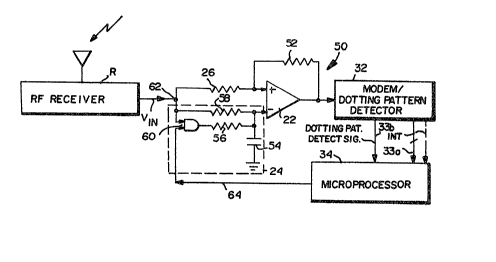
Figure 5 is a schematic diagram o~ the
presently preferred exemplary embodiment of an
adaptive limiter circuit 50 in accordance with the
present invention. Limiter circuit 50 includes a
comparator 22, a RC network 2~, an additional series
input resistor 26, a feedback resistor 52, and a
modem/dotting pattern detector 32.
The limiter circuit 50 is connected to
receive an incoming signal Vin (e.g., a demodulated
version of the channel assignment request message ~2
shown in FIGURE 4~ produced by conventional RF
receiver R, this incoming signal typically including a
digital signal stream superimposed upon a shifting DC
level. Limiter circuit 50 processes the incoming
signal stream and generates a version of the stream
which it applies to modem/dotting pattern detector 32.
Incoming digital signal stream Vin is
connected through input resistor 26 to the
non-inverting input terminal of comparator 22. A
feedback resistor 52 is connected between the
comparator non-inverting input and the comparator
,
, : - . ,
.
16 - 45MR 508
output terminal. The output terminal of compara-tor 22
is connected to the input of modem/dotting pattern
detector 32 which converts the incoming serial bit
stream to parallel format and communicates the
resulting parallel digital information to the input of
microprocessor 34 over line 33a. Modem/dot-tiny
pattern detector 32 also detects the alternatiny
binary valued Os and ls of the dotting pattern
preceding each incoming message (e.g., using
lo conventional hard-wired detection logic) and produces
a signal on line 33b indicating a predetermined number
of bits of dotting pattern have been detected. Modem
32 and/or microprocessor 34 also decodes other
portions of the incoming digital data.
RC network 24 includes a capacitor 54, a
resistor 56, a resistor 58 and a gate ("switching
means") 60. Resistor 58 is connected directly between
the Vin output of receiver R and the comparator 22
inverting input. Capacitor 54 is connected between
the comparator inverting input and ground (reference)
potential.
Gate 60 in the preferred embodiment is a
two-input CMOS AND (or other logic type) gate having a
first input terminal connected to Vin and a second
input terminal connected to an output line 64 of
microprocessor 34 (or line 33b produced by
modem/dotting pattern detector 32 may be connected
directly to this input of gate 60). The output
terminal of gate 60 is connected to one end of
resistor 56. The other end of resistor 56 is
connected to the comparator inverting input.
The resistance of resistor 56 is much lower
than that of resistor 58. When microprocessor 34
applies a logic level 1 signal (via line 64) to the
input of gate 60, the gate turns ON to effectively
12~2~:~L7
- 17 - 45MR 508
place resistor 56 in parallel with resistor 58 --
decreasing the time constant of RC network 24.
In the preferred embodiment the lowest
frequency component in the dotting pattern preceding
each incoming message is ~.8 KHz, while the lowest
frequency component in received digital dat~ (e.g.,
word sync pattern) following the dotting pattern is
about 1o Hz. In the preferred embodiment, RC network
24 has a time constant of 0.33 milliseconds during the
- 10 time a dotting pattern is expected to be received
(this time constant corresponding to a cut-off
frequency of about 3 KHz) -- that is, during the time
no message is being received (but the receiver is
"listening" for a new message) and during the time the
initial portion of a new incoming message is being
decoded. At other times (i.e., during the time the
word sync and data of a message is being received and
detected), RC network 24 has a time constant on the
order of 0.1 seconds (corresponding to a cut-off
frequency of about 10 Hz).
In one exemplary circuit the capacitance of
capacitor 54 is about 1 microfarad, the value of
resistor 58 is on the order o~ 100 Kilohms and the
value of resistor 56 is on the order of about 330
ohms.
When the signal level present on
microprocessor output lines 64 is at logic level 0,
gate 60 does not turn ON regardless of the level of
input signal Vin, and resistor 56 is effectively
disconnected from limiter circuit 50 -- so that the
time constant o~ RC network 24 is on the order of 0.1
seconds. When microprocessor output line 64 is active
(i.e., at a logic level 1 signal level), gate 60 turns
on whenever the level of signal Vin is above the
input threshold level of the gate and resistor 56 is
- - ~ - - . - -
. . .
.. : , . , . . . -
. -' ~ ' ,, ' '
'.
.
- . . . - . . - .
~82~L7
- 18 - 45MR 508
thus effectively placed in parallel with resistor 58
-- decreasing the time constant of RC network 2~ to
about 330 microseconds.
FIGURE 6 is a flow chart of exemplary
program control steps executed by microprocessor 34
(under software control) to detect and decode dottiny
pattern and other incoming digital data and also to
control RC network 24. The flow shown in flow chart
24 is from top to bottom, beginning at "start" block
10 100.
Microprocessor 34 first determines whether
an incoming signal has been received (decision block
102) -- typically by waiting for a so-called
"interrupt" signal generated by modem/dotting pattern
detector 32 whenever an incoming signal is sensed at
the output of the receiver R. During (and before)
this time, microprocessor 34 causes its output line 6
to be active -- so that resistor 56 is connected in
parallel with resistor 58 and RC network 24 has a time
constant of about 330 microseconds.
When a signal has been received,
microprocessor 34 (or a hard-wired detection circuit
of modem/dotting detector 32) detects whether the
received signal is a dotting pattern (that is, a
stream of alternating binary valued digital signals
(block 104). During the time this initial portion of
the incoming message is being received and detected,
limiter circuit 50 adapts very rapidly to the DC
component on which the dotting pattern is superimposed
-- resulting in dotting pattern detection in 10
milliseconds or less. If a dotting pattern has been
received (indicated by an active signal level on line
33b), microprocessor 34 places a logic level 0 signal
level on output line 64 to inhibit gate 60 and thereby
effectively disconnect resistor 56 from RC network 24
. .
~8~7
- 19 - 45MR 508
(block 106) -- switching the time constant of the RC
network to about 0.1 seconds. Meanwhile,
modem/dotting pattern detector 32 has already acquired
bit synchronization (in a conventional manner) in
response to the received dot-ting pattern and is ready
to synchronously receive the Barker code word
synchronization pattern following the dottiny
pattern. The lowest frequency components of the
Barker code (and the digital data signals following
it) are passed by limiter 50 because of the large
limiter bandwidth resulting from disconnection of
resistor 56.
Microprocessor 34 (and/or modem/dotting
pattern detector 32) acquires word (frame)
synchronization in response to receipt of a Barker
code and proceeds to process the incoming signal
stream (block 110) (e.g., if the received data is
digital word synchronization codes, detector 32 or
microprocessor 34 detects the word sync codes and
acquires frame synchronization from them in
preparation for receiving a digital message which
follows). Limiter circuit 50 passes all of the lower
frequency components of this received digital stream
(e.g., down to 10 Hz) because RC network 24 has a
large time constant.
When a message has terminated (as indicated,
for example, by discontinued receipt of incoming its
tested for by block 108), microprocessor 34 applies a
logic level 1 signal to output 64 (block 112) to once
again enable gate 60 -- thus connecting resistor 56
back into RC network 24. When gate 60 is enabled in
this manner, RC network 24 again has a time constant
of only 330 microseconds -- and is capable of adapting
very rapidly to the DC component superimposed on the
dotting pattern preFeding the next message to be
. - - :
.
- 20 - 45MR 508
received. Gate 60 is enabled in the preferred
embodiment at all times except during the execution
of blocks 106-lI0 of the FIGURE 6 flow chart (i.e.,
until after the dotting pattern of a new message has
been successfully decoded), so that resistor 56
remains connected in circuit with RC network 2~ when
the next dotting pattern is received.
FIGURE 7 is a graphical illustration of the
time it takes the limiter circuits shown in FIGURES 2
lo a~d 5 to adapt to an inco~ing message transmission.
The curve labelled "A" is the actual receiver DC bias
point (i.e., the level of the DC component upon which
the incoming digital signal stream is superimposed).
As can be seen, the actual DC bias point rises sharply
initially upon receipt of a carrier signal, soon
thereafter demonstrates a "hump" during which time the
receiver locks onto the transmit carrier frequency,
and finally stabilizes approximately 20 milliseconds
after first receipt of the signal.
The prior art limiter shown in FIGURE 2 is
not capable of tracking the rapidly changing DC bias
level during the first 20 milliseconds of signal
reception because its time constant is too slow (slow
enough to pass signal low frequency components but
too slow to track the rapidly changing signal level).
The curve marked "B" in FIGURE 5 shows the value of
the voltage across capacitor 54 (the adaptive
threshold level) in the FIGURE 2 limiter. This
adaptive threshold level does not closely match the
actual DC bias level until the received signal has
"stabilized" -- about 20 milliseconds after signal
- receipt. Detection of incoming digital signals is not
possible until this 20 millisecond delay is over.
The curve marked "C" in FIGURE 7 shows the
voltage across capacitor 54 of the FIGURE 5 limiter
' ' ~' ','' ~ '' : ,
., :
- 21 - 45MR 508
circuit 50 provided by the present invention. Because
the RC time constant o~ network 24 is relatively short
(330 microseconds in the preferred embodiment) during
the time the dotting pattern at the beginning of the
new message is received, limiter circuit 50 very
rapidly adapts to the actual DC bias level, and begins
closely tracking the actual bias level in as little as
lO milliseconds or less after receipt of the incoming
signal. Proper detection of the dotting pattern
preceding the message (and acquisition of bit
synchronization i response to this dotting pattern) is
rapid and occurs as early as lO milliseconds or less
after the first bit of the dotting pattern is
received.
The limiter circuit provided by the present
invention has significant advantages over the prior
art limiter circuit. Because the preferred embodiment
limiter circuit very rapidly adapts to the DC bias
component superimposed upon the received digital
signal, the receiver can detect the dotting pattern in
a much shorter time than could receivers in the prior
art. The duration of the dotting pattern may thus be
decreased substantially, reducing signalling
"overhead" and providing more time for transmission of
useful data signals.
For example, if a time-division multiplexed
l'slotted" (or other timing critical) control channel
is used in a trunking radio telephone communications
system to convey control information between
transceivers and a repeater as shown in FIGURES 3 and
4, acquisition signals must be transmitted on the
I'inbound'' control channel in a "slot" (time period) of
limited duration (e.g., 30 ms). If the receiver
requires a long time period to acquire bit
synchronization little time remains within the time
.. , . ' - ' ' '' ~ : .
~,~8~
- 22 - 45MR 508
slot for transmission of acquisition or other contact
signals. If the duration of the time slot is
increased, loading capacity of the channel is
decreased proportionally -- and the entire system
cannot handle as much message traffic. Accordingly,
it is desirable to minimize the duration of the time
slot.
- The present invention accomplishes exactly
that by allowing receivers to detect the dotting
pattern message preamble even before the DC bias level
of the repeater receiver has "stabilized". In
addition, the repeater receiver processes a received
signal only after successfully receiving and decoding
dotting pattern, falsing rate is decreased
substantially over that obtainable simply by using
Barker code or other word sync pattern detection as in
the Butcher et al arrangement -- and detection of the
Barker code (word sync) can be improved since not all
of the bits of the Barker code need to be properly
detected in order to obtain proper word
synchronization (compare this with the Butcher et al
scheme, which requires proper detection of the entire
word sync pattern before the limiter RC time constant
is increased).
While the present invention has been
describecl with what is presently considered to be the
most practical and preferred embodiments, it is to be
understood that the appended claims are not to be
limited to the disclosed embodiments, but on the
contrary, they are intended to cover all
modifications, variations and/or equivalent
arrangements which retain any of the novel features
and advantages of this invention. By way of
non-limiting example, although the preferred
embodiment uses a gate 60 to switch resistor 56 into
- -, :
- ' :
.. ' ' ' : ~ .
~ad~7
- 23 - 45MR 508
and out of RC network 24, other suitable switching
means (e.g., a switching capacitor, a translstor, or
even a relay) could be used as if desired.
' - ' ' ' . , ' ' , ' ~
- ~
.
,. : - - .