Note: Descriptions are shown in the official language in which they were submitted.
.
~8~L51
TEX/2921lCft
Microprocessor Back-up System
The present invention concerns back-up stores
for the main processors of digital telephone exchanges.
Back-up stores are used to maintain essential data in
the event of the main processor malfunctioning. In the
event of such a malfunction the back-up system stores
billing data, operating system data and exchange
configuration data.
So far the provision of back-up storage has
involved the use of static memories such as bubble-
; 10 memories with their very low current and voltage
requirements. However, bubble-memories also have
limitations with regard to size. Also the access time
to bubble-memories is relatively slow.
The present invention has for an object to
1~ provide an alternative form of back~up storage.
Accordingly the present invention consists in
a back-up system for the main processor of a digital
telephone exchange, the system comprising a storage
array of CMOS dynamic RAM's, means for detecting failure
in the normal power supply, means for switching from
the normal power supply to a secure back-up supply on
detection of failure of the former, and means for
providing a regular refresh of the storage array after
such switchlng has taken place.
~ 1 A
, -2-
Preferably the back-up system includes a micro-
processor controlling read/write operation from and into
the CMOS storage array and the back-up system includes
means for providing a burst or rapid refresh as soon as
power failure is detected, and for periodic, cyclical
refresh of the CMOS array thereafter.
According to a feature of the invention the
array is arranged in a plurality of banks, and the CMOS
devices of one bank only are refreshed at any one time
of the refresh cycle.
In order that the present invention may be more
readily understood, an embodiment thereof will now be
- described by way of example and with reference to the
accompanying drawings, in which
Figure 1 is a block diagram of the change over
and refresh logic of a back-up system for the main
processor of a digital telephone exchange according to
the present invention,
Figure 2 is a block diagram showing the
power up/power down signal interface, and
Figure 3 is a block diagram of the entire back-up
system.
Referring now to Figure 1 of the drawings, the
first function of the control circuitry shown in this
Figure is to detect failure of the exchange processor.
The cause of failure for which the back-up store is
intended is that of the processor power supply which is
unsecured. The condition of this supply is detected at 10
and supplied in parallel with +5V battery source 11 to
a monostable 12. The response of monostable 12 is tuned
by a delay circuit 13 to produce a 3 microsecond delay.
On triggering of the monostable 12 an output pulse is
generated on line 15. Line 15 is connected to a memory
sequencer built from two logic arrays which control
read/write operations not required during back-up. The
-3-
signal on line 15 terminates current operation after
allowing the memory sequencer to finish. Line l5 is
the path for resetting the power down refresh logic in
preparation for takeover from the unsecured power supply.
The power down refresh circuit is generally
indicated at 20 and includes a 4 MegaHertz CMOS
oscillator 21 which provides a base clock for the sy3tem
and from which the various clock signals are ~er:ived by
a counter chain 22. One output from counter chain 22
is on line 23 and this is supplied to one input of a
flip-flop 24 which changes between burst refresh and
lower power refresh at the end of the count from the
counter chain 22. The burst refresh of the CMOS back-up
store RAM is carried out quickly, making the best possible
use of the failing unsecured power supply, in order to
ensure that each row address receives a ll ms type refresh
before the 32 ms type refresh without an intervening
read or write cycle~ The reset pulse for flip-flop 24
is taken from output line 15 from monostable 12.
Line 15 is connected to the clock input of a
D-type flip-flop 50 and causes a signal referred to as
PFAILDIS to clock low. PFAILDIS appears at the Q output
of flip-flop 50 and is connected to selector circuit 17.
When PFAILDIS goes low, selector circuit 17, which is
a quad 2 to 1 multiplexer, goes into its back-up mode
and generates a clear signal on line 16 which is supplied
to the CLEAR input of monostable 12 to ensure that the
latter takes no further notice of signals appearing on
line 10.
PFAILDIS, as well as changing selector circuit 17
into back-up mode, also inhibits Write and Column Address
strobes to the CMOS dynamic store. This means that the
data in the back-up store remains unchanged. PFAILDIS
also inhibits routine testing of the unit back-up battery
which takes place during normal operation.
, -4-
The signal on line 15 is also supplied to a
flip-flop 24 having two control inputs and when low
sets flip-flop 24 into burst-refresh mode. The rea~ons
for burst-refresh have already been described. To do
this the Q outpuk of flip-flop 24 is connected via a
line 60 to the SELECT input of a selector circuit 61~
Selector circuit 61 in respon~e to the signal from flip-
flop 24 uses a 2 MegaHertz clock signal derived from a
4 MegaHertz oscillator 21 to generate Row Address Strobe
(RAS) pulses which act through circuit 17, already in
back-up mode, to drive the RAS generation circuitry.
The output of oscillator 21 is supplied to a 12 stage
binary counter chain 22 having three effective outputs~
Q1 at 2 MegaHertz, Q2 at 1 MegaHertz and Q12 at 1 KiloHertz.
The Q1 output is used for burst-refresh and passes
through selector circuit 61 to circuit 17 where it emerges
to be carried by line 80 to the appropriate RAS control
circuitry to be described later in this specification.
In response to the pulse chain selector 17 also provides
refresh control pulses on line 81. The counter chain 22
is reset by a pulse in line 14 from monostable 12 and
provides the various clock signals for the system. The
output f`rom Q12 appears at the end of the count from
counter chain 22 and is supplied to the RESET input of
flip-flop 24. The appearance of this signal changes the
flip-flop 24 from the burst-refresh mode instigated by
the pulse on line 15 into lower power refresh. In this
mode the output of flip-flop 24 sets selector 61 to
accept the 1 MegaHertz input from counter chain 22 and
supplies the 1 MegaHertz signal to a divider chain 62.
The output of divider chain 62 is supplied to
a passive delay line driver 65 in turn connected to a
passive delay line 64 with the output of delay line 64
being connected to one input of an AND-gate 70, the
other input of which is the direct output of divider
chain 62. The effect of this circuit is to generate a
--5--
chain of pulses having 160 microseconds ~idth, which
pulse chain passes straight through selector circuit 61
to selector circuit 17. The latter circuit has already
been set in its power fail mode and the pulse chain is
used to drive the refresh circuitry and row address
control.
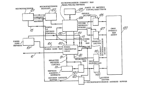
Referring now to Figure 2 of the drawings, this
shows the entire power up/down signal interface in
greater detail. The block shown in this drawing at 100
effectively consists of the circuit elements 12, 13, 17
and 50 of Figure 1, and comprises the po~Jer changeover
logic whilst block 101 includes the remaining circuit
elements of Figure 1. Thus line 15 is duplicated in
both figures as is line 80 on which the RAS control
pulses appear, and line 81 for the refresh control
pulses. In Figure 2 the line 101 represents the various
clock signals derived from counter chain 22 of Figure 1.
Line 80 is connected to a RAS sequency circuit 110
which controls the supply of Row Address Strobes to the
CMOS dynamic RAM array 120. Line 81 is connected to a
circuit 111 which generates the addresses to which
refresh pulses are to be applied and to the enable input
of a refresh address buffer 112. The buffer 112 is
connected to an address driver circuit 113 in turn
connected to the array 120.
The circuit shown in ~igure 2 also includes a
microprocessor 121 ~hich controls the back-up store
during normal, power-up, operation. In normal operation,
that is until it is inhibited by the signal on line 15,
this circuit sends commands and addresses to a micro-
processor support circuit 122, and the addresses to a
microprocessor address buffer 123 effectively connected
in parallel with refresh address buffer 112, the output
of buffer 123 also being connected to address driver
circuit 113.
--6-
Microprocessor support circuit 122 has its output
connected to a circuit 124 which under the ti~ing control
of a circuit 125 supplies Column Address Strobes (CAS)
to a driver circuit 126, and Write Enable signals to
another driver circuit 127. When power failure has been
detected the P~AILDIS signal inhibits the driver circuits
126, 127 and microprocessor address buffer 123 so that
no new data is written into or read from array 120 and
only the refresh, write RAS and CA,S pulses of the access
in progress are allowed to reach array 120.
The circuit 124 during power-up operation supplies
control slgnals on line 130 to the power changeover logic
circuit 101. When the unsecured power supply has failed
so that power-down operation has started RAS pulses on
line 131 from circuit 124 are inhibited.
Referring now to Figure 3 of the drawings this
shows at 150 the unsecured supply used in normal, power-up
operation. Also shown is the secure, battery-backed
supply 151. Circuit elements shown in common with
Figures 1 and 2 have the same reference numerals. Also
shown is a multibus interface 152 and a SCSI (Small
Computer Systems Interface) 153 which is used to drive
a hard disc store. The CMOS array 120 comprises 8 banks
of 256 kilowords by 1 dynamic CMOS RAM's. Each bank
contains 17 dynamic RAM's, giving a total of 136 devices.
The array can store two megawords with each word being
defined as 16 bits of data plus 1 parity bit. The CMOS
technology gives low power consumption together with
fast access times.
In the present embodiment the refresh time for
a particular row within a device in the array is
32 milliseconds when in the battery backed-up mode.
Because of power restrictions the logic of the refresh
circuitry is such that in back-up mode refresh is
performed on only one bank at any one time.
5~
.. .
--7--
Pages written in the array 120 are protected
against corruption during power-down because all page
dumps are performed in two parts. The data is first
written into a temporary page and then trasnferred to
the destination page. A flag is set before the second
transfer by the microprocessor 121. If power fails
during this second transfer then the system will examine
the flag when power returns and re-perform the transfer
if necessary. This ensures that a RAM page either
remains unwritten or is completely overwritten with valid
data.