Some of the information on this Web page has been provided by external sources. The Government of Canada is not responsible for the accuracy, reliability or currency of the information supplied by external sources. Users wishing to rely upon this information should consult directly with the source of the information. Content provided by external sources is not subject to official languages, privacy and accessibility requirements.
Any discrepancies in the text and image of the Claims and Abstract are due to differing posting times. Text of the Claims and Abstract are posted:
| (12) Patent: | (11) CA 1282182 |
|---|---|
| (21) Application Number: | 578837 |
| (54) English Title: | SUBSTRATE CONNECTOR GUIDE |
| (54) French Title: | GUIDE DE CONNEXION POUR SUBSTRAT |
| Status: | Deemed expired |
| (52) Canadian Patent Classification (CPC): |
|
|---|---|
| (51) International Patent Classification (IPC): |
|
| (72) Inventors : |
|
| (73) Owners : |
|
| (71) Applicants : | |
| (74) Agent: | R. WILLIAM WRAY & ASSOCIATES |
| (74) Associate agent: | |
| (45) Issued: | 1991-03-26 |
| (22) Filed Date: | 1988-09-29 |
| Availability of licence: | N/A |
| (25) Language of filing: | English |
| Patent Cooperation Treaty (PCT): | No |
|---|
| (30) Application Priority Data: | None |
|---|
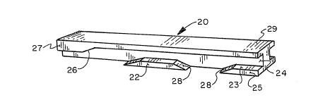
SUBSTRATE CONNECTOR GUIDE
ABSTRACT
A substrate connector guide for installing and
electrically connecting an electrical substrate to a carrier
substrate. The substrate connector guide includes a plurality
of guide rails mounted on the perimeter edge of the electri-
cal substrate and at least a first electrical connector
mounted transversely between the guide rails. First and
second substrate guides are mounted to the carrier substrate
in a spaced and parallel relationship to the other. Each
substrate guide includes a channel extending longitudinally
along a substrate guide inner side, from an open end to a top
guide. The channel is further defined by a top surface and a
plurality of drop guides which in turn form a plurality of
slots. At least a second electrical connector is mounted and
electrically connected to the carrier substrate between the
first and second substrate guides. The electrical substrate
is installed by manually inserting the electrical substrate
into respective substrate guide open ends and manually
pushing the electrical substrate along the channels until the
substrate encounters a respective top guide. The top guides
then urge the substrate downward until each electrical
substrate guide rail falls into a respective substrate guide
slot. Each of the electrical substrate's plurality of guide
rails rest on the carrier substrate and align the first
electrical connector to the second electrical connector. An
electrical connection is completed between the electrical
substrate and the carrier substrate when the electrical
substrate is fully seated on the first and second substrate
guides.
Note: Claims are shown in the official language in which they were submitted.
Note: Descriptions are shown in the official language in which they were submitted.
For a clearer understanding of the status of the application/patent presented on this page, the site Disclaimer , as well as the definitions for Patent , Administrative Status , Maintenance Fee and Payment History should be consulted.
| Title | Date |
|---|---|
| Forecasted Issue Date | 1991-03-26 |
| (22) Filed | 1988-09-29 |
| (45) Issued | 1991-03-26 |
| Deemed Expired | 2001-03-26 |
There is no abandonment history.
| Fee Type | Anniversary Year | Due Date | Amount Paid | Paid Date |
|---|---|---|---|---|
| Application Fee | $0.00 | 1988-09-29 | ||
| Registration of a document - section 124 | $0.00 | 1989-02-14 | ||
| Maintenance Fee - Patent - Old Act | 2 | 1993-03-26 | $100.00 | 1993-02-25 |
| Maintenance Fee - Patent - Old Act | 3 | 1994-03-28 | $100.00 | 1994-03-02 |
| Maintenance Fee - Patent - Old Act | 4 | 1995-03-27 | $100.00 | 1995-02-27 |
| Maintenance Fee - Patent - Old Act | 5 | 1996-03-26 | $150.00 | 1996-02-28 |
| Maintenance Fee - Patent - Old Act | 6 | 1997-03-26 | $150.00 | 1997-03-25 |
| Maintenance Fee - Patent - Old Act | 7 | 1998-03-26 | $150.00 | 1998-03-23 |
| Maintenance Fee - Patent - Old Act | 8 | 1999-03-26 | $150.00 | 1999-03-15 |
Note: Records showing the ownership history in alphabetical order.
| Current Owners on Record |
|---|
| GTE COMMUNICATION SYSTEMS CORPORATION |
| Past Owners on Record |
|---|
| BELANGER, THOMAS D., JR. |

