Note: Descriptions are shown in the official language in which they were submitted.
i . I
BACKGROUND OF THE INVENTION
*
This invention relates generally to a process for
fabricating an integrated circuit, and more particularly ko an
improved method for fabricating metal interconnections in a
semiconductor integrated circuit.
Aluminum and aluminum alloys are the most common materials
used to fabricate metal contacts and interconnections in an
integrated circuit built on a silicon substrate. These metals
have several advantages over other conductive materials, most
importantly, because of their low resistivity which results in
an increase in device operating speed. In addition, these
metals are relatively soft and flexible and, therefore, bond
well to underlying layers and tend not to lift off. Aluminum
is also a relatively inexpensi~e material.
However, the use of aluminum is not without its drawbacks.
For example, aluminum spiking into the substrate may occur.
Moreover, hillocking on the aluminum layer can be induced by
thermal cycling during various processes, such as a
high-temperature anneal step after the aluminum is deposited.
This leads to reduced reliability and greater processing
difficulties. In double level metal processes, for example,
large hillocks can cause shorts between aluminum layer~.
Hillocks may also cause difficulties in photolithographic
definition of fine lines due to irregular reflections.
It is known that the use of a refractory metal as the top
,
layer of the metallization layer will reduce the likelihood of
hillock formation on an aluminum layer. Howe~er, this can
result in difficulties during final packaging, as refractory
metals are brittle and are not easily processed at low
temperatures, and therefore do not bond easily to gold or
" ~ .
, - 2 -
` !
aluminum bonding wires. As a result, it is necessary to remove
the upper refractory metal at the location of the bonding
pads. This has, however, in the past required the performance
of an additional photolithographic step or the formation o~ an
additional metal layer of aluminum over the upper refractor~
metal layer.
It is an object of the present invention to provide a
metallization process which allows contact to be made to the
bonding pads during the fabrication of a semiconductor
integrated circuit without the requirement of an additional If
photolithographic operation.
It is a further object of the present invention to provide
an improved metallization process of the type described, which
reduces significantly the formation of hillocks in the metal
contacts and interconnections and substantially eliminates
aluminum spiking.
.
. ! SUMMARY OF THE INVENTION
!
To these ends, the invention provides a process for
depositing and etching metal contacts and interconnections in a
semiconductor integrated circuit. The metal is deposited as a
sandwich structure consisting of a refractory metal, aluminum
or aluminum alloy, and a refractory metal. This configuration
of the metallization layer minimizes hillocking and eliminates
aluminum spiking. After an overlay oxide and/or nitride is
deposited over the sandwich metallization structure and etched
at the locations of the bonding pads, the top layer of
refractory metal exposed at the bonding pads is etched off in a
plasma etcher without the need for an additional photolitho-
graphic operation, so as to improve the adhesion of gold or;
aluminum wires to the bonding pads during packaging of t~;e
integrated circuit.
-- 3 --
2~L88
6~538-965
In summary, the present invention provides a ~ethod of
making a metal connection to the fa~e of a semi~onducto~ body, the
connection extending over a step in an insulatincJ layer on the
face, said method comprising: (a) providiny a semiconductor
substrate; (b) forming a three-layer sandwi~h structure of me-tal
by depositing a layer of a refractory metal, a layer of alurninufn
or aluminum alloy, and a layer of refractory metal over said
substrate; (c~ selectively removing said three-layer sandwich
structure; (d) depositing a protective oxide and~or nitride
overlay layer over the remaining portions of said three-layer
metal sandwich structure; (e) etching an opening to the bonding
pad in said protective overlay layer; and (f) employing the
remaining overlay layer as an etchant mask, and wlthout using an
additional lithography stepr selectively removing by clry etching
the refractory metal layer at the bonding pad to expose the
underlying aluminum or aluminum alloy.
3a
32~3L8~ ,
., i,
BRIEF DESCRIPTION OF THE DRAWINGS
~ !
To the accomplishment of t}le above and such further objects
as may hereinafter appear, the present invention relates to a
process for forming a metallization pattern in an integrated
circuit substantially as defined in the appended claims and as
described in the following detailed specification, as
considered in conjunction with the accompanying-drawings in
Which
Figures la-le are cross sections of a semiconductor
integrated circuit fabricated in accordance with the present
invention shown in various stages in the fabrication process,
leading up to the final structure illustrated in Figure le.
DETAILED DESCRIPTION OF THE INVENTION
In the exemplary embodiment of the invention illustrated in
the figures, the process of the invention is described in '
connection with the fabrication of a CMOS device. It will be
understood, however, that the process of the invention may also
be used to comparable advantage in the fabrication of NMOS and
PMOS devices.
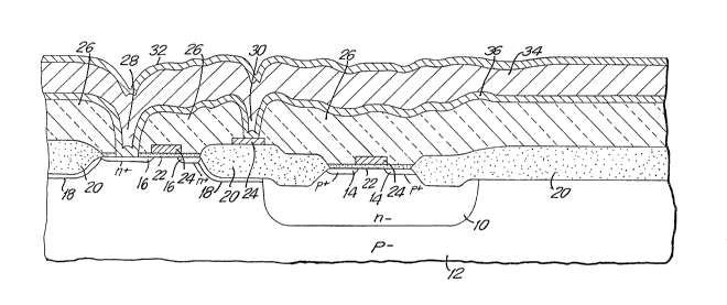
Referring first to Fig. la, an n-well 10 is formed in any
known manner in the upper surface of a substrate 12 here shown
as being of p+ conductivity. CMOS transistors are formed in
the silicon wafer by doping with boron or boron difluoride ions
to form p+ regions 14 in the n-well 10 and by doping with
arsenic or phosphorus ions to form n+ regions 16 in the p-type
substrate 12. As is also conventional, a p~ field implant 18
is performed, a field oxide layer 20 and a gate oxide 22 are
grown, and polysilicon regions 24 are deposited and
preferentially etched to form the gate regions of the MO~
_ 4 _
~ x~z~a~ i
. ' .
transistOrs and other conductive areas. A ~lass layer 26 is
deposited over ~his structure and contact openings 28 and 30
are selectively etched in the glass layer.
- A multilayer metallization layer is then deposited over
this structure. As shown in Fig. la, the metalli~ation
structure consists of a 200-2000 A layer of titanium 32 over an
approximately 1.0 micron layer 34 of aluminum - 1% silicon.
Underlying the aluminum layer 34 is a 1200-2000-A layer of
titanium 36. Other re~ractory metals besides titanium and
their alloys and aluminum alloys may also be used in the
metallization sandwich structure. The initial or~underlying
layer 32 of re~ractory metal or refractory metal alloys
prevents aluminum spiking into the silicon substrate. The
upper refractory metal layer 36 suppresses the formation of
hillocks in the intermediate aluminum or aluminum alloy layer
34, which is undesirable in single metal processes because of
reduced reliability and greater processing difficulties, and is
additionally undesirable in double metal processes because of
the risk of shorts between two aluminum layers.
Thereafter, as shown in ~ig. lb, a photoresist is patterned
and the metal layers 32, 34 and 36 are etched to create the
metal pattern illustrated in Figure lb to define the location
of an interconnect 38 and a bonding pad 40. The etch used in
this step is preferably an anisotropic reactive ion etch
employing chlorine~based chemistry so that the metal is mostly
removed vertically, and slightly horizontally.
If the MOS device is to employ a single metal layer, an
overlay oxide and/or nitride layer 42 is deposited in a PECVD
system, as illustrated in Fig. lc. Layer 42, which may be
approximately 8000 A thick, serves as a passivation layer for
the device. An anisotropic, vertical orientation-dependçnt;
~Z8Z18~3
reactive ion e~ch which utilizes fluorine-based chemistry is
then used to create an opening 44 in layer 42 to the bonding
pad 40 as shown in Fig. ld.
Finally, to improve the adhesion of gold or aluminum
bonding wires to the bonding pad, the upper refractory titaniurn
metal layer 32 on top of the bonding pad is removed to allow
gold or aluminum bonding wires to be bonded to the exposed
aluminum layer 34. The removal of the upper titanium layer is
preferably achieved through the use of a dry etch employing
fluorine-based chemistry, at a power of between 900 and 1500
watts, a pressure of between 80 and 125 mTorr, and a flow rate
of SF6 of between 80 and 120 sccm. The removal o the
overlying titanium layer 32 in this manner, which is accom-
plished without the need for any additional photolithographic
step, results in the structure illustrated in Fig. le.
Although this invention has been described with regard to a
speciic embodiment for illustrative purposes, this description
is not meant to be limiting. For example, it will be apparent
to those skilled in the art that the process of this invention
may be used with other integrated circuit fabrication
techniques. It is also believed apparent that modifications to
the inventive process described hereinabove may be made by
those skilled in the art without necessarily departing from the
spirit and scope of the invention.
. ~
.
'