Note: Descriptions are shown in the official language in which they were submitted.
3~
-- 1 --
TITLE OF THE IWVENTION
LOW-PITCHED SOUND CI~EATOR
B~CKGROUND OF THE INVBNT ION
This invention relates to a low-pitched sound
creator which can improve an aural sensation in low-pitched
sound reproduced by an audio system, an audio-visual
system, or the like. This invention also relates to a
method of creating a low-pitched sound.
Some sound reproducing devices have a head deriving
and reproducing a sound signal from sound data stored in a
magnetic memory such as a magn-etic tape. Reproducing heads
have characteristics causing low-pitched sound cut-off
frequencies. Specifically, these heads fail to acceptably
reproduce original sound signals in frequency ranges below
such cut-off frequencies.
Advanced sound reproducing systems have an
additional function of compensating for poor low-pitched
sound reproducing characteristics of heads.
SUMM~RY OF THE INVENTION
It is an object of this invention to provlde a
low-pitched sound creator or a;sound signal processing
device which can improve an aural sensation in low-pitched
sound reproduced by an audio system, an audio-visual
system, or the like.
~5 It is another object~of this invention to provide a
:: :
.
-- 2 --
method which allows an excellent aural sensation in
low-pitched sound.
In a low-pitched sound creator according to a first
aspect of this invention, an analog sound signal is
outputted. Low-frequency components are selected ~rom the
outputted analog sound signal so that a low-pitched sound
signal is derived from the analog sound signal. A key of
the low-pitched sound signal is lowered so that a
very-low-pitched sound signal is derived from the
low-pitched sound signal. The analog sound signal and the
very-low-pitched sound signal may be converted into
corresponding sounds respectively.
In a low-pitched sound creator accor~ ng to a second
aspect of this invention, two channel sound signals are
outputted. A subtraction between the two channel signals
is derived and thereby a subtraction signal indicative
thereof is generated. The two channel signals are added to
form a mixed signal. A first low-pass filter selects
low-frequency components from the subtraction signal and
thereby generates a first low-pitched sound signal
representing the selected low-frequency components of the
subtraction signal. A second low-pass filter selects
low-Erequency components from the mixed signal and thereby
generates a second low-pitched sound signal representing
the selected low-frequency components of the mixed signal.
Z34~
-- 3
A Xey of the first low-pitched sound signal is lowered so
that a very-low-pitched sound signal is derived from the
first low-pitched sound signal. An envelope of the second
low-pitched sound signal is detected. The very-low-pitched
sound signal is selectively passed and cut off in
accordance with the detected envelope.
In a low-pitched sound creator according to a third
aspect of this invention, an analog sound signal is
outputted. First and second low pass filters haviny
different cut-off frequencies derive ~irst and second
low-pitched-sound signals from the analog sound signal
respectively. Arbitrary one of the first and second
low-pitched sound signals is selected. A key of the
selected low-pitched sound signal is halved so that a
lS key-halved signal is derived from the selected low-pitched
sound signal.
In a low-pitched sound creator according to a fourth
aspect of this invention, two channel sound signals are
outputted. A subtraction between the two channel signals
is derived and thereby a subtraction signal indicative
thereof is generated. The two channel signals are added to
form a mixed signal. A device detects whether or not the
two channel signals contain voice components. Arbitrary
one of the subtraction signal and the mixed signal is
selected in accordance with whether or not the two channel
':
:-
3~
signals contain voice components, and a selected signalrepresenting the selected one of the subtraction signal and
the mixed signal is generated. A low-pass filter selects
low-frequency components from the selected signal and
thereby generates a low-pitched sound signal representing
the selected low-frequency components. A key of the
low-pitched sound signal is halved so that a
very-low-pitched sound signal is derived from the
low-pitched sound signal.
In a method of creating a low-pitched sound
according to a fifth aspect of this invention,
low-frequency components are selected from a sound signal.
A key of the selected low-frequency components is lowered.
The key-lowered components are converted into a
corresponding sound.
BRIEF DESCRIPTION OF THE DRAWINGS
Fig. 1 is a block diagram of a conventional audio
system.
Fig~ 2 is a graph showing frequency characteristics
of the reproducing device of Fig. 1.
Fig. 3 is a block diagram of another conventional
audio system.
Fig. 4 is a block diagram of an audio system
including a low-pitched sound creator according to a first
embodiment of this lnvent-on.
3~L
-- 5
Fig. ~ is a graph showing frequency characteristics
of the reproducing device and the audio system of Fig. 4.
Fig. 6 is a block diagram of an internal structure
of the key converter of Fig. 4.
Fig. 7 is a diagram of an essential portion of the
internal structure of the key converter of Figs. 4 and 6.
Fig~ 8 is a block diagram of an audio system
including a low-pitched sound creator according to a second
embodiment of this invention.
Fig. 9 is a block diagram of an audio system
including a low-pitched sound creator according to a third
embodiment of this invention.
Fig. 10 is a block diagram of an audio system
including a low-pitched sound creator according to a fourth
embodiment of this invention.
Fig. 11 is a block diagram of an audio system
including a low-pitched sound creator according to a fifth
embodiment of this invention.
Fig. 12 is a block diagram of an audio system
including a low-pitched sound creator according to a sixth
embodiment of this invention.
Flg. 13 is a block diagram of an internal structure
of the level determination circuit of Fig. 12.
Fig. 14 is a block diagram of an audio system
2S including ~ lo~-pitched sound cr-a-or according to a
.
:
. .
Vs~
-- 6 --
seventh embodiment of this invention.
Fig. 15 is a block diagram of an audio system
including a low-pitched sound creator according to an
eighth embodiment of this invention.
Fig. 16 is a block diagram of an audio system
including a low pitched sound creator according to a ninth
embodiment of this invention.
Fig. 17 is a block diagram of an audio system
including a low-pitched sound creator according to a tenth
embodiment of this invention.
Fig. 18 is a block diagram of an audio system
including a low-pitched sound creator according to an
eleventh embodiment of this invention.
Fig. 19 is a block diagram of an internal structure
of the detector of Fig. 18.
Like and corresponding elements are usually denoted
~y the same reference characters throughout the drawings.
DESCRIPTION OF T~E PREFERRED EMBODIMENTS
-
Before embodiments of this invention will be
e~plained, conventional audio systems will be described
briefly for a better understanding of this invention.
Fig. 1 shows a conventional audio system having a
reproducing device 81 such as a tape deck or a radio
receiver. An output signal Sl from the reproducing device
81 is magnified by an amplifier 82 and is then converted by
34~
a loudspeaker 83 into a corresponding sound M.
The tape deck 81 has a head deriving and reproducing
a sound signal Sl from sound data stored in a magnetic tape
or the like. Fig. 2 shows frequency characteristics of the
tape deck 81 which depend mainly on frequency
characteristics of the reproducing head. In Fig. 2, the
voltage level of the sound signal Sl varies as a function
o~ the frequency of the sound signal S1 along the line L1.
At frequencies above a low-pitched sound cut-off frequency
fl, the tape deck 81 has essentially flat frequency
characteristics. As the frequency decreases from the
cut-off value fl, the level of the sound signal S1 drops.
The hatched area A1 denotes an unproduced ranye having
frequencies below the cut-off frequency fl.
As is understood from Fig. 2, the conventional audio
system of Fig. 1 can not acceptably reproduce sounds having
frequencies lower than the cut-off frequency fl.
Fig. 3 shows another conventional audio system also
having a reproducing device 81. An output signal Sl from
the reproducing device 81 is applied vla a branching device
88 to an amplifier 82 and a low-pass filter (LPF) 84.
After the sound signal Sl is ampllfled~by the` device 82, it
is converted into a corresponding sound b~ a loudspeaker
83. The low-pass filter 84 derives a~low-pitched sound
signal S2 from the sound slgnal~S1. For example, the
:
- ' '' . '.. :'
.
r~3~
-- 8 --
low-pitched sound signal S2 have frequencies equal to or
below 150 Hz. After the low-pitched sound signal S2 is
magnified by an amplifier 86, it is converted into a
corresponding sound by a loudspeaker 87.
The conventional audio system of Fig. 3 can
compensate for poor low-pitched sound reproducing
characteristics of the reproducing device 81 to some
extents. If an original sound signal fails to have
low-frequency components, sounds reproduced by the audio
system of Fig. 3 will not have corresponding low-pitched
components.
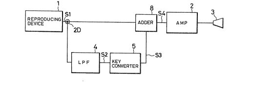
Fig. 4 shows an audio system including a low-pitched
sound creator according to a first embodiment of this
invention. As shown in Fig. 4, the audio system has a
reproducing device 1 such as a tape deck or a radio
receiver. An output terminal of the reproducing device l
i5 connected to an input terminal of a branching device 2D.
A first output terminal of the branching device 2D is
connected to a first input terminal of an adder 8. A
second output terminal of the branching device 2D is
connected to an input terminal of a low-pass filter (LPF)
4. An output signal Sl from the reproducing device l is
applied via the branching device 2D to the first input
terminal of the adder 8 and to the input terminal of the
low-pass filter 4.
3 ~3X3~a~
g
I'he low-pass filter 4 selects low-frequency
components from the sound signal Sl and thereby derives a
low-pitched sound signal S2 from the signal Sl. A cut-off
frequency of the low-pass filter 4 is preferably around 150
Hz. An output terminal of the low-pass filter 4 is
connected to an input terminal of a key or pitch converter
5 so that the output signal S2 from the low-pass filter 4
is applied to the key converter 5. The key converter 5
serves as a frequency lowering converter. Thus, the key
converter 5 lowers the frequencies or pitches of the signal
S2 outputted by the low-pass filter 4. Preferably, this
device 5 converts the low-pitched sound signal S2 into a
second low-pitched sound slgnal S3 having frequenies half
the respèctive frequencies of the corresponding sound
signal S2. In other words, the low-frequency components of
the sound signal Sl selected by the low-pass filter 4 are
lowered in frequency by a value corresponding to an octave.
In this way, a very-low-pitched sound signal S3 is derived
from the low-pitched sound signal S2.
2~ It should be noted that the key converter 5 may
decrease the frequencies of the low-pitched sound signal S2
by other factors. For example, the frequencies of the
very-low-pitched sound signal 53 may be one-third or
one-fourth of the respective frequencies of the low-pitched
sound signal S2.
X3~
-- 10 --
An output terminal of the key converter 5 is
connected to a second input terminal of the adder 8 so that
the very-low-pitched sound signal S3 is applied to the
second input terminal of the adder 8. The sound signal Sl
and the very-low-pitched sound signal S3 are added by the
device 8 to form a processed or modified sound signal S4.
~n output terminal of the adder 8 is connected to an input
terminal of an amplifier 2 so that the modified sound
signal S4 is applied to the amplifier 2. An output
terminal of the amplifier 2 is connected to a loudspeaker
3. After the modified sound signal S4 is amplified by the
device 2, it is converted into a corresponding sound by the
loudspeaker 3.
Fig. 5 shows frequency characteristics of the
reproducing device 1 and frequency characteristics of the
audio system of Fig. 4. In Fig. 5, the broken line Nl
denotes low frequency characteristics of the reproducing
device 1, while the solid line N2 denotes low frequency
characteristics of the audio system of Fig. 4. The hatched
area L2 between the lines Nl and N2 denotes an added
low-frequency reproduced range created by the sound signal
processing through the key converter 5. A low cut-off
frequency f2 in the frequency characteristics of the audio
system of Fig. 4 is lower than a low cut-off frequency fl
in the frequency characteristics of the reproducing device
823~D~
1 by a value corresponding to an octave. The added
low-frequency reproduced range L2 improves an aural
sensation in respect of low-pitched sounds. Furthermore,
even in cases where sound signals lack very-low-frequency
components, e.g., even in the case of an AM radio
broadcasting sound signal or a movie sound signal, the
sound signal processing through the key converter 5 creates
very-low-frequency components from a base sound signal and
adds them to the base sound signal to form a modified sound
signal rich in low-frequency components, so that an
e~cellent aural sensation is allowed in respect of
low-pitched sounds.
- Fig. 6 is a block diagram of an internal structure
of the key converter 5. As shown in Fig. 6, the key
converter 5 has an input terminal 101 subjected to a
low-pitch sound signal S2 outputted by the low-pass filter
4 (see Fig. 4). An analog-to-digital (A/D) converter 102
derives a one-bit digital signal D0 from the input analog
signal S2 through adaptive delta modulation. This adaptive
delta modulation uses a syllable compander which depends on
whether or not four successive one-bit digital signals are
in the same state. A dynamic random-access memory 10~
holds the digital signaI D0. A first digital-to-analog
(D/A) converter 105 derives an analog signal S6 from a
one-bit digital signal Dl outputted by the memory 104. A
' ~ '
' , ' ' ' .:
9.~823~
second digital-to-analog (D/A) converter 118 derives an
analog signal S7 from a one-bit digital signal Dl outputted
by the memory 104. An adder 116 derives a very-low-pitched
sound signal S3 from the analog signals S6 and S7 outputted
by the D/A converters 105 and 118. Specifically, the
analog signals S6 and S7 from the D/A converters 105 and
118 are added by the device 116 to form a very-low-pitched
sound signal S3. The very-low-pitched sound signal S3 is
transmitted to an output terminal 106 of the key converter
5.
A generator 108 outputs clock pulses D2 at a fixed
frequency. A generator 110 derives conversion clock pulses
f0 from the fixed-frequency clocks D2. The conversion
clocks f0 are applied to the A/D converter 102. The A/D
converter 102 samples and converts the low-pitched sound
signal S2 at timings determined by the conversion clocks
f0.
Operation of the digital memory 104 is controlled in
accordance with various signals including a row address
~0 strobe (RAS) signal, a column address strobe (CAS) signaI,
a write enable (WE) signal, a write address signal, and a
read address signal.
A write address caunte~r 112 derives a slgnal D4 from
the fixed-frequency clocks D2. This signal D4 represents a
write address. The write address signal D4 is applied to
323~fl~
- 13 -
the memory 104. The current incoming digital signal D0 is
transmitted to and held by a segment of the memory 104
corresponding to the address represented by the write
address signal D4.
A generator 109 outputs clock pulses D7 at a
variable frequency. A generator 111 derives a memory
control signal D3 from the fixed-frequency cloc~s D2 and
the variable-frequency cLocks D7. The memory control
signal D3 is applied to the memory 104. Specifically, the
memory control signal D3 includes the RAS signal, the CAS
signal, and the WE signal.
A generator 113 derives write address counter load
signals ~5 and D9 from the fixed-frequency clocks D2. A
first read address counter 114 derives a signal D6 from the
write address signal D4, the read address counter load
signal D5, and the variable-frequency clocks D7. This
signal D6 represents a first read address. The first read
address signal D6 is applied to the memory 104. Data is
read out from a segment of the memory 104 corresponding to
the first read address represented by the signal D6.
second read address counter 120 derives a signal D8 from
the write address signal D4, the read address counter load
signal D9, and the variable-frequency clocks D7. This
signal D8 represents a second read address~ The second
read address signal D8 is applied to the memor~ 104. Data
' ' ' , ,
' . . '
. .
'
32~
- 14 -
is read out from a segment of the memory 104 corresponding
to the second read address represented by the signal D8.
The first read address signal D6 and the second read
address signal D~ are generally designed to occur
alternately at regular intervals.
A generator 115 derives conversion clock pulses fv
from the variable-frequency clocks D2. The conversion
clocks fv are applied to the D/A converters 105 and 118.
The D/A converters 105 and 118 sample and convert the
memory output digital signal Dl at timings determined by
the conversion clocks fv.
Data writing to the memory 104 is performed
periodically at a frequency determined by the
fixed-frequency clocks D2. Data reading from the memory
104 is performed periodically at a frequency determined by
the variable-frequency clocks Fv. The ratio between the
pitches of the key-converter input and output signals S2
and S3 is generally proportional to the ratio between the
frequencies of the data writing and reading.
A counter 140 derives an amplitude operation signal
from the variable-frequency clocks D7. The amplitude
operation signal is applied to an operation device 141.
The operation device 141 derives first and second multi-bit
digital signals from the amplitude operation signal. The
first multi-bit signal from the operation device 141 is
.
,
.. : .
.
~ ' .
8;23~
- 15 -
applied to a first data selector 143. The second multi-bit
signal from the operation device 141 is applied to a second
data selector 149. The fixed-frequency clocks D2 are
applied to the data selectors 143 and 149. The first data
selector 143 sequentially selects one bit data of the first
multi-bit signal from the calculation device 141 in
accordance with the fixed-frequency clocks D~. The second
data selector 149 sequentially selects one bit data of the
second multi-bit signal from the calculation device 141 in
accordance with the fixed-frequency clocks D2.
The output signal from the first data selector 143
is applied to a first input terminal of an AND gate 144.
The first D/A converter 105 includes a circuit deriving or
detecting a syllable compander digital signal. This
compander signal generated in the first D/A converter 105
is applied to a second input terminal of the AND gate 144.
A signal outputted by the AND gate 144 is applied to the
first D/A converter 105. The first D/A converter 105 also
includes a circuit adjustably controlling or limiting the
amplitude of the output signal 56. The signal fed to the
first D/A converter 105 from the AND:gate 144 adjusts the
limiting circuit so that the amplitude of the~signal S6 is
controlled in accordance with the signal from the AND gate
144. ~ ~ :
The output signal from the second data selector 149
~:
~ :: :
,
,
-' ' ' ' ' ~ ~ : `
~;23~
- 16 -
is applied to a first input terminal of an AND gate 150.
The second D/A converter 118 includes a circuit deriving or
detecting a syllable compander digital signal~ This
compander signal generated in ~he second D/A converter 118
is applied to a second input terminal of the AND gate 150.
A signal outputted by the AND gate 150 is applied to the
second D~A converter 118. The second D/A converter 118
also includes a circuit adjustably controlling or limiting
the amplitude of the output signal S7. The signal fed to
the second D/A converter 118 from the AND gate 150 adjusts
the limiting circuit so that the amplitude of tAe signal S7
is controlled in accordance with the signal from the AND
gate 150.
The amplitude controls of the signals S6 and S7 are
designed to remove or prevent noises caused by
discontinuities in waveforms occurring during sound pitch
changing process. In general, such noises occur at known
regular timings. In view of this fact, the combination of
the devices 140, 141, 143, 144, 149, and 150 performs the
amplitude controls of the signals S6 and S7 in
time-dependent manner.
The output signal S6 from the first D/A converter
105 is periodically enabled and nullified. The output
signal S7 from the second D/A converter 118 is periodically
enabled and nullified. Approximately, the signal S6 is
8~3~
- 17 -
enabled but the signal S7 is nullified during a ~irst
period, and the signal S6 is nullified but the signal S7 is
enabled during a subsequent second period. Near the
boundary between the first and second periods, the
amplitudes of the signals S6 and S7 are controlled in a
cross fade-in/fade-out manner. Specifically, near the
boundary between the first and second periods, one of the
signals S6 and S7 is gradually enabled while the other is
gradually nullified. These controls of the signals S6 and
S7 are realized through the amplitude controls by the
combination`of the devices 140, 141, 143, 144, 149, and
150.
Fig. 7 is a diagram of an essential portion of the
key converter of Fig. 6. As shown in Fig. 7, an output
signal Dl from the memory 104 (see Fig. ~) is applied to a
data input terminal of a shift register 124 via a
connection point 123. ~ latch clock signal fv derived from
the variable-frequency clocks D7 is applied to a control
terminal of the shift register 124 via a connection point
22. The shift register 124 has a set of four positive ox
non-inverting output terminals Ql-Q4 generating four
signals D14-D17 respectively and a set of four negative or
inverting output terminals Ql-Q~ generating four signals
D18-D21 respectively. The output signals D14-D21 shift
with respect to the output terminals at timings determined
.
~X~3~3~A~
- 18 -
by the latch clock signal fv.
The output signals D14-D17 ~rom the shi~t register
124 are applied to four input terminals of a NAND gate 125
respectively. The other output signals D18-D21 from the
shift register 124 are applied to four input terminals of a
NAND gate 126 respectively. An output signal D22 from the
NAND gate 125 is applied to a first input terminal of a
NAND gate 127. An output signal D23 from the NAND gate 12
is applied to a second input terminal of the NAND gate 127.
An output signal D24 from the NAND gate 127 assumes a high
or "1" level state only when all of the signals D14-D17 - -
simultaneously assume the same state. Accordingly, only in
the case where four or more successive signals Dl outputted
from the mèmory 104 (see Fig. 6) are in the same state, the
output signal D24 from the NAND gate 127 assumes a high or
"1" level state. In this way, a syllable compander signal
D24 is derived which is used to control adaptive operation.
The adaptive control signal D24 is applied to the second
input terminal of the AND gate 144.
The output signal D14 from the shift register 124 is
applied to a data input terminal of a custom IC (~or
example, "M5225L" made by Mitsubishi Electric Corporation)
128 forming a digital-to-analog converter. The second pin
of the IC 128 is grounded by a fixed resistor 129 and a
capacitor 134. A constant voltage is applied to the
,
. . .
,. ~ .
~'~8~3a~
-- 19 --
junction between the resistor 129 and the capacitor 134 via
a fixed resistor 135. The collector of a transistor 131 is
connected via a fixed resistor 130 to the junction between
the resistor 129 and the capacitor 134. The emitter of the
transistor 131 is grounded. The base o~ the transistor 131
is grounded via a fixed resistor 133. An output signal D30
from the AND gate 144 is applied to the base of the
transistor 131 via a fixed resistor 132. A parallel
combination of a ~ixed resistor 136 and a capacitor 137 is
10 connected between the sixth pin and the seventh pin of the .
IC 128. Thè seventh pin of the IC 128 outputs a signal S6
wh.ich is applied via a connection point 138 to the adder
116 (see Fig. 6).
The D/A converter 105 (see Fig. 6) includes the
shift register 124, the NAND gates 125-127, the IC 128, the
transistor 131, the resistors 129, 130, 132, 133, 135, and
136, and the capacitors 134 and 137. The output digital
signal Dl from the memory 104 (see ~ig. 6) is converted
into a corresponding analog signal S6 which is outputted
via the connection point 138.
The variable-frequency clocks D7 are applied to the
amplitude operation counter 140 via a connection point 139.
The counter 140 derives an amplitude operation signal D26
from the variable-frequency clocks D7. The amplitude
operation signal D26 is applied to the operation device
,
.
3~L
- 20 -
141. The operation device 141 derives a multi-bit digital
signal D27 from the amplitude operation signal D26. The
multi-bit signal D27 from the operation device 141 is
applied to the first da'a selector 143. The
i fi~ed-frequency clocks D2 are applied to the first data
selector 143 via a connection point 142. The device 143
sequentially selects one bit of the multi-bit digi-tal
signal D27 in accordance with the fixed-frequency clocks
D2. The first data selector 143 outputs a signal D29
reflecting the selected data. The signal D29 is applied
to the first input terminal of the AND gate 144.
While the adaptive operation control signal D24
remains in a high or "1" level state, the AND gate 144 iS
opened so that a high or "1" level pulse signal D29 from
the first data selector 143 iS allowed to move to the base
of the transistor 131 as an output signal D30 from the AND
gate 144. When the high level signal D30 is applied to the
base of the transistor 131, the transistor 131 is made
conductive, discharging the capacitor 134 and decreasing
the voltage at the junction between the capacitor 134 and
the resistor 129. A drop in the voltage at the junction
between the capacitor 134 and the resistor 129 generally
causes a decrease in the voltage of the analog signal S6.
In this way, the amplitude of the output analog signal S6
is controlled in accordance with the slgnals D24 and D29.
.
.
~ ~3234~
Specifically, the duration of the high or "1" level pulse
D29 determines the amplitude of the output analog signal
S6. The combination of the devices 140, 141, and 143
varies the duration of the high or "1" level pulse D29 in
time-dependent manner so as to perform desired
~ade-in/fade-out control of the amplitude of the output
analog signal S6.
The operation device 141 also generates a second
multi-bit digital signal in accordance with the amplitude
operation signal D26. The second multi-bit signal is
applied to the second data selector 149 (see Fig. 6). The
second multi-bit signal is generally similar to the
multi-bit signal applied to the first data selector 143.
The combination of the second D/A converter 118 (see
Fig. 6), the second data selector 149 (see Fig. 6), and the
AND gate 150 (see Fig. 6) is similar to the combination of
the first D/A converter 105r the first data selector 143,
and the AND gate 144 except for the following point. The
second data selector 149 sequentially selects one bit of
the multi-bit signal from the operation device 141 in a
reverse or opposite order with respect to the data
selection order in the first data selector 143.
Accordingly, the output analog signal S7 undergoes amlitude
fade-in/fade-out control opposite that of the other output
analog signal S6.
. ,
'' '
323~
- 22 -
It should be noted that the key converter 5 of Figs.
6 and 7 is one example, although it is not prior art. The
key converter 5 may also be of any known types.
Fig. 8 shows a second embodiment of this invention
which is similar to the embodiment of Figs. 4-7 except for
the design changes indicated below.
The adder 8 (see Fig. 4) is omitted from this
embodiment. The branching device 2D is directly coupled to
the amplifier 2 so that the sound signal Sl from the
reproducing device 1 is applied to the input terminal of
the amplifier 2. Accordingly, the sound signal Sl is
converted into a corresponding sound by the loudspeaker 3.
The output terminal of the key converter 5 is
connected to an input terminal of an amplifier 6 so that
the very-low-pitched sound signal S3 is applied to the
amplifier 6. An output terminal of the amplifier 6 is
connected to a loudspeaker 7, such as a woofer. After the
very-low-pitched sound signal 53 is amplified by the device
6, it is converted by the loudspeaker 7 into a
corresponding sound.
Fig. 9 shows a third embodiment of this invention.
As shown in Flg. 9, in thls embodiment, a~ reproducing
device la outputs a first channel signal SL and a second
:
channel signal SR. A first~channel output termlnal of the
reproducing device la ls connected to;an lnput terminal of
:
:
.
:: . .
- . . : . ,
' , ' ' ' ' , , ' ' ~' ' ' , " ' ,
.
,.' ' "' ' ' ''
~B'~34~
- 23 -
a first branching device lL so that the first channel
signal SL is applied to the first branching device lL. A
second channel output terminal of the reproducing device la
is connected to an input terminal of a second branching
device lR so that the second channel signal SR is applied
to the second branching device lR.
A first output terminal of the first branching
device lL is connected to an input terminal of an amplifier
2L. A second output terminal of the first branching device
lL is connected to a first input terminal oE an operation
or calculation circuit 10. The first channel signal SL
from the reproducing device la is applied to the amplifier
2L and the operation circuit 10 via the first branching
device lL.
An output terminal of the amplifier 2L is connected
to a loudspeaker 3L. After the branched first channel
signal SL is amplified by the device 2L, it is converted by
the loudspeaker 3L into a corresponding sound.
A first output terminal of the second branching
device lR is connected to an input terminal of an amplifier
2R. A second output terminal of the second branching
device lR is connected to a second inpu-t terminal of the
operation circuit 10. The second channel signal SR from
the reproducing device la is applied to the amplifier 2R
and the operation circuit 10 via the second branching
3234~
- 24 -
device lR.
An output terminal of the amplifier 2R is connected
to a loudspeaker 3R. ~fter the branched second channel
signal SR is amplified by the device 2R, it is converted by
the loudspeaker 3R into a corresponding sound.
The operation circuit 10 includes a subtractor or
difference calculator which outputs a signal S8
corresponding to a difference between the first channel
signal SL and the second channel signal SR. The operation
circuit 10 may include additional devices which adjust
phases and ievels of the two signals SL and SR so as to
minimize the level of the output signal S8.
An output terminal of the operation circuit 10 is
connected to an input terminal of a low-pass filter (LPF) 4
so that the signal 58 is applied to the low-pass filter 4.
The low-pass filter 4 selects low-frequency components from
the signal S8 and thereby derives a low-pitched signal S9
from the signal S8. A cut-off frequency of the low-pass
filter 4 is preferably around 150 Hz.
An output terminal of the low-pass filter 4 is
connected to an input terminal of a key or pitch converter
5 so that the output signal S9 from the low-pass filter 4
is applied to the key converter 5. The key converter 5
serves as a frequency Iowering converter. Preferably, this
device 5 converts the low-pitched signal S9 into a second
.
" ,. ~ . ,~ ,, '
.- ~ ~ . ', : ' .
3Z3~
- 25 -
low-pitched signal S10 having frequenies half the
respective frequencies of the corresponding signal S9. In
other words, the low-frequency components of the signal S8
selected by the low-pass filter 4 are lowered in frequency
by a value corresponding to an octave. In this way, a
very-low-pitched signal S10 is derived from the low-pitched
signal S9.
It should be noted that the key converter 5 may
decrease the frequencies of the low-pitched signal S9 by
other factors. For example, the frequencies of the
very-low-pitched signal S10 may be one-third or one-fourth
o the respective frequencies of the low-pitched signal S9.
The key converter 5 is preferably similar to that of
Figs. 6 and 7. The key converter 5 may also be of known
types.
An output terminal of the key converter 5 is
connected to an input terminal of an amplifier 6 so that
the very-low-pitched signal S10 is applied to the amplifier
6~ An output terminal of the amplifier 6 is connected to a
~0 loudspeaker 3W such as a woofer or a super woofer. After
th~ very-low-pitched signal S10 is amplified by the~device
6, it is converted by the loudspeaker 3W into a
corresponding sound.
It was experimentally found that if a sound signal
having vocal or voice components was subjected to key down
- 26 -
process, the resulting signal and the corresponding
reproduced sound tended to be distorted. In general, the
two channel signals SL and SR contain vocal or voice
components at essentially the same level and the same
phase. In view of these facts, subtraction between the two
channel signals SL and SR is performed by the operation
circuit 10 to derive a signal S8 essentially free from
vocal or voice components~ After this signal S8 is treated
by the low-pass filter 4, it is subjected to key down
process in the pitch converter 5. In this way, a signal
essentially free from vocal components is subjected to key
down process, so that the resulting signal and the
corresponding reproduced sound less tend to be distorted.
Fig. 10 shows a fourth embodiment of thls invention
which is similar to the embodiment of Fig. 9 except for the
following design changes.
As shown in Fig. 10, the output terminal of the
low-pass filter 4 is connected to an input terminal of a
branching device 12D. A first output terminal of the
branching device 12D is connected to a first input terminal
of an adder 9. A second output terminal of the branching
device 12D is connected to the input terminal of the key
converter 5. The output signal S9 from the low-pass filter
4 is applied to the first input terminal of the adder 9 and
the key converter 5 via the branching device 12D. The
.
~L~8'~3f~
- 27 -
output terminal of the ~ey converter 5 is connected to a
second input terminal of the adder 9 so that the output
signal S10 from the key converter 5 is applied to the
second input terminal of the adder 9.
In this way, one branched signal S9 bypasses the key
converter 5, while the other branched signal S9 is
subjected to key down process in the pitch converter 5.
The key converter 5 derives the very-low-pitched signal S10
from the inputted branched signal S9. The very~low-pitched
signal S10 and the branched signal S9 are added by the
device 9 to form a signal Sll.
An output terminal of the adder 9 is connected to
tha input terminal of the amplifier 6 so that the output
signal Sll from the adder 9 is applied to the amplifier 6.
After the signal Sll is amplified by the device 6, it is
converted by the loudspeaker 3W into a corresponing sound~
Fig. 11 shows a fifth embodiment of this invention
which is similar to the embodiment of Fig. 9 except for the
following design changes.
As shown in Fig~ 11, a branching device 12L is
interposed between the branching device lL and the first
input terminal of the operation circuit 10. Specifically,
an input terminal of the branching device 12L is connected
to the branching device lL so that the first channel signal
SL is applied to the input terminal of the branching device
23~~
-- 28 --
12L. A first output terminal of the branching device 12L
is connected to the first input terminal of the operation
circuit 10. A second output terminal of the branching
device 12L is connected to a first input terminal of an
adder 9F. The first channel signal SL is applied via the
branching device 12L to the operation circuit 10 and the
adder 9F.
Another branching device 12R is interposed between
the branching device lR and the second input terminal of
the operation circuit 10. Specifically, an input terminal
of the branching device 12R is connected to the branching
device lR so that the second channel signal SR is applied
to the input terminal of the branching device 12R. A first
output terminal of the branching device 12R is connected to
the second input terminal of the operation circuit 10. A
second output terminal of the branching device 12R is
connected to a second input terminal of the adder 9F. The
second channel signal SR iS applied via the branching
device 12R to the operation circuit 10 and the adder 9F.
The first channel signal SL and the second channel~
signal SR are added by the dev1ce 9F to form a signal S12.
An output terminal of the adder:9F is connected to an input
terminal of a low-pass filter ~LPF)~13 so:that the signal
S12 is applied to the low-pass filter 13~ The low-pass
filter 13 selects low-frequency components from the signal
::
:
, '
`' ' '
234
-- 29 --
S12 and thereby derives a low-pitched signal S13 from the
signal S12.
An output terminal of the low-pass filter 13 is
connected to a first input terminal of an adder 9B so that
the low-pitched signal S13 from the low-pass filter 13 is
applied to the first input terminal of the adder 9B. The
adder 9B is interposed between the key converter 5 and the
amplifier 6. The output terminal of the key converter 5 is
connected to a second input terminal of the adder 9B so
that the very-low-pitched signal S10 is applied to the
second input terminal of the adder 9B. The low-pitched
signal S13 and the very-low-pitched signal S10 are added by
the device 9B to form a signal Sll.
An output terminal of the adder 9B is connected to
the input terminal of the ampli`fier 6 so that the signal
Sll is applied to the amplifier 6. After the signal Sll is
amplified by thP device 6, it is coverted by the
loudspeaker 3W into a corresponding sound.
Fig. 12 shows a sixth embodiment of this invention
which is similar to the embodiment of Fig. 11 except for
the following design changes. In the embodiment of Fig.
12, a branching arrangement 3D represents the combination
of the branching devices lL, lR, 12L, and 12R (see Fig.
11) .
The adder 9B (see Fig. 11) is omitted from the
.
3;23~4
- 30 -
embodiment of Fig. 12. A switching circuit ll and a level
determination circuit 14 are added to the embodiment of
Fig. 12.
As shown in Fig. 12, the switching circuit 11 is
connected between the output terminal of the key converter
5 and the input terminal of the amplifier 6. When the
switching circuit ll is closed, the very-low-pitched signal
SlO from the key converter 5 is allowed to travel to the
input terminal of the amplifier 6. When the switching
circuit ll is opened, the application of -the
very-low-pitched signal SlO to the amplifier 6 is
interrupted. The switching circuit ll has a control
terminal. The switching circuit ll is closed and opened in
accordance with a potential at its control terminal.
The output terminal of the low-pass filter 13 is
connected to an input terminal of the level determination
circuit 14 so that the output signal Sl3 from the low-pass
filter 13 is applied to the level determination circuit 14.
The level determination circuit 14 generates a binary
signal Sl4 which depends on the amplitude of the input
signal Sl3. Specifically, the signal Sl4 moves between a
first level state and a second level state in accordance
with whether or not the amplitude of the signal Sl3 exceeds
a reference level. An output terminal of the level
determination circuit 14 is connected to the control
? '
.
4~
- 31 -
terminal of the switching circuit 11 so that the signal S14
from the level determination circuit 14 is applied to the
control terminal of the switching circuit 11.
When the amplitude of the signal S13 exceeds the
reference level, the signal S14 assumes a first level
state, opening the switching circuit 11 and thereby
interrupting the application of the very-low-pitched signal
S10 to the amplifier 6. Accordingly, in this case, the
very-low-pitched signal S10 is not converted into a sound.
When the amplitude of the signal S13 is equal to or
lower than the reference level, the signal S14 assumes a
second level, closing the switching circuit 11 and thereby
applying the very-low-pitched signal S10 to the amplifier
6. Accordingly, in this case, the very-low-pitched signal
S10 is converted into a corresponding sound by the
loudspeaker 3W.
A cut-off frequency of the low-pass filter 13 is
lower than the cut-off frequency of the low-pass filter 4.
The cut-off frequency of the filter 13 is generally higher
than half the cut-off frequency of the filter ~. In the
case where the filters 4 and 13 have sharp frequency
characteristics, the cut-off frequency of the fil~er 13 is
preferably half the cut-off frequency of the filter 4.
The combination of the adder 9F, the low-pass filter
13, and the level determination circuit 14 essentially
~,.
34fl~
-- 32
serves to determ~ne whether or not at least one of the two
channel signals SL and SR originally contains appreciable
amounts of very-low-pitched sound components. When at
least one of the two channel signals SL and SR originally
contains appreciable amounts of very-low-pitched sound
components, the switching circuit 11 is opened by the
signal S14 from the level determination circuit 14 so that
the very-low-pitched signal S10 derived through key down
process is prevented from changing to a sound.
If at least one of the two channel signals SL and SR
originally contained appreciable amounts of
very-low-pitched sound components and the pitch-converted
signal S10 containing created very-low-pitched sound
components was changed to a sound, the original
very-low-pitched sound components and the created
very-low-pitched sound components would interfere with each
other and thereb~ unacceptable distortions would occur. In
this embodiment, such unacceptable distortions are
prevented, since the conversion of the very-low-pitched
signal S10 to a corresponding sound is interrupted when at
least one of the two channel signals SL and SR originally
contains appreciable amounts of very-low-pitched sound
components.
Fig. 13 shows an internal design of the level
determination circuit 14. As shown in Fig. 13, the level
~ " ~
~a~3~
- 33 -
determination circuit 14 includes an input terminal 14A
subjected to the signal S13 from the low-pass filter 13.
The input terminal 14A is connected to an input terminal of
an envelope detector or integrator 15 so that the signal
S13 is applied to the device 15. The integrator 15
generates a signal S15 which depends on the amplitude of
the input signal S13. Specifically, the signal S15
reflects an envelope of the signal S13. Accordingly, the
level of the signal S15 corresponds to the ampli.tude of the
signal S13. An output terminal of the integrator 15 is
connected to a first input terminal of a comparator 16 so
that the envelope signal S15 is applied to the first input
terminal of the comparator 16. A level setting circuit 17
outputs a reference level signal S16. An output terminal
of the level setting circuit 17 is connected to a second
input terminal of the comparator 16 so that the reference
level signal S16 is applied to the second input terminal of
the comparator 16. The comparator 16 generates a binary
signal S14 in accordance with the input signals S15 and
~0 S16. Specifically, when the level of the envelope signal
S15 exceeds a reference level represented by the signal
S16, the signal S14 assumes a first level state. When the
level of the envelope signal S15 is equal to or lower than
the reference level, the signal S14 assumes a second level
state. An output terminal of the comparator 16 is
3~
- 34 -
connected to a connectlon point 14s leading to the control
terminal of the switching circuit 11 (see Fig. 12).
Accordingly, the output signal S14 from the comparator 16
is transmitted to the switching circuit 11 via the
connection point 14B.
Fig. 14 shows a seventh embodiment of this invention
which is similar to the embodiment of Figs. 12 and 13
except for the following design changes.
As shown in Fig. 14, the output terminal of the
low-pass filter 4 is connected to an input terminal of a
branching device 12D. A first output terminal of the
branching device 12D is connected to the input terminal of
the key converter 5. A second output terminal of the
branching device 12D is connected to a first input terminal
of an adder 18. The output signal S9 from the low-pass
filter 4 is applied via the branching device 12D to the key
converter 5 and the first input terminal of the adder 18.
The output terminal of the key converter 5 is
connected to a second input terminal of the adder 18 so
that the very-low-pitched signal S10 from the key converter
5 is applied to the second input terminal of the adder 18.
The low-pitched signal S9 from the low-pass filter 4 and
the very-low-pitched signal S10 from the key aonverter 5
are added by the device 18 to form a signal S17. An output
terminal of the adder 18 is connected to the input terminal
,
~L~ ~X 3 ~
of the switching circuit 11 so that the signal S17 is
applied to the switching circuit li. The switching circuit
11 ena~les and interrupts the application of the signal S17
to the amplifier 6 in accordance with the signal S14.
Fig. 15 shows an eighth embodiment of this invention
which is similar to the embodiments of Figs. 12 and 13
e~cept for the following desing changes.
As shown in Fig. 15, the output terminal of the
adder gF is connected to an input terminal of a branching
device 12F. A first output terminal of the branching
device 12F is connected to the input terminal of the
low-pass filter 13. A second output terminal of the
branching device 12F is connected to an input terminal of a
low-pass filter (LPF) 19. The output signal S12 from the
adder 9F is applied via the branching device 12F to the
low-pass filters 13 and 19. The low-pass filter 19 selects
low-frequency components from the signal S12 and thereby a
low-pitched signal Sl9 from the signal S12.
The output terminal of the switching circuit 11 is
connected to a first input terminal of an adder 20 so that
an output signal S18 from the switching circuit 11 is
applied to the first input terminal of the adder 20. An
output terminal of the low-pass filter 19 is connected to a
second input terminal of the adder 20 so that an output
slgnal fr~om the 1ow-~ss~ ~iltcr 19 is applied to the second
'
234~
- 36 -
input terminal of the adder 20. The signals S18 and Sl9
are added b~ the device 20 to form a signal S20. An output
terminal of the adder 20 is connected to the input terminal
of the amplifier 6 so that the signal S20 from the adder 20
is applied to the amplifier 6.
Fig. 16 shows an audio system including a
low-pitched sound creator according to a ninth embodiment
of this invention. As shown in Fig. 16, the audio system
has a reproducing device 1 such as a tape deck. The
reproducing device 1 has a control terminal subjected to a
binary control slgnal D. The reproducing device 1 assumes
either of a normal speed state and a double speed state in
accordance with the control signal D. The reproducing
speed in the double speed state is twice the reproducing
speed in the normal speed state.
~ he output terminal of the reproducing device 1 is
connected to an input terminal of a branching device 30D so
that the output signal Sl from the reproducing device 1 is
applied to the branching device 30D. A ~irst output
terminal of the branching device 30D is connected to an
input terminal of a low-pass filter (LPF) 22. A second
output terminal of the branching device 30D is connected to
an input terminal of a low-pass filter (LPF) 23. A third
output terminal of the branching device 30D is connected to
a first input terminal 29A of a switching circuit 29. The
~8~3
-- 37 --
output sound signal Sl from the reproducing device 1 is
applied via the branching device 30D to the low-pass
filters 22 and 23, and the first input terminal 29A of the
switching circuit 29.
The low-pass filter 22 selects low-frequency or
low-pitched sound components from the sound signal Sl and
thereby derives a low-pitched sound signal S21 from the
signal Sl. An output terminal of the low-pass filter 22 is
connected to a first input terminal 24A of a switching
circuit 24 so that the low-pitched sound signal S21 is
applied to the first input terminal 24A of the switching
circuit 24.
The low-pass filter 23 has a cut-off frequency
higher than a cut-off frequency of the low-pass filter 22.
The low-pass filter 23 selects audible-frequency or audio
components from the sound signal Sl and thereby derives an
audio signal S22 from the signal Sl. An output terminal of
the low-pass filter 23 is connected to a second input
terminal 24B oE the switching circuit 24 so that the audio
signal S22 is applied to the second input terminal 24B of
the swithcing circuit 24.
An output terminal 24~ of the switching circuit 24
is connected to an input terminal of a key or pitch
converter 5 so that an output signal S23 from the switching
circuit 24 is applied to the key converter 5. The
34~
- 38 -
switching circuit 24 has a control terminal subjected to
the binary control signal D. The switching circuit 24
passes either of the low-pitched signal S21 and the audio
signal S22 to the key converter 5 in accordance with the
control signal D.
The key converter 5 serves as a frequency lowering
converter. In other words, the key converter 5 lowers the
frequencies or pitches of the signal S23 outputted by the
switching circuit 24 and selected from either of the
10 low-pitched sound signal S21 and the audio signal S22. ,
Specifically, this device 5 converts the signal S23 into a
signal S24 having frequenies half the respective
frequencies of the corresponding sound signal S23. In
other words, the signal S23 is }owered in frequency by a
value corresponding to an octave. In this way, a
frequency-halved~sound signal S24 is derived from the
signal S23 outputted by the switching circuit:24.
The key converter 5 is preferably similar to that of
Figs. 6 and 7. The key converter 5 may also be of known
~0 types. :
The switching circuit 2~ has a control terminal
subjected to the binary control signal~ D. The:switching
: : :
circuit 29 selectively passes and cuts off the:sound signal
Sl in accordance with the control signal D.
An output terminal 29C of the switching circuit 29
- : : :
. .'.'
; ~ " , '
. .
3~
- 39 -
is connected to a first input terminal of an adder 26 so
that an output signal S25 from the switching circuit 29 is
applied to the first input terminal of the adder 26. An
output terminal of the key converter 5 is connected to a
second input terminal of the adder 26 so that the
frequency-halved signal S24 is applied to the second input
terminal of the adder 26. The signal S25 from the
switching circuit 29 and the signal S24 from the key
converter 5 are added by the device 26 to form a signal
S26.
An oùtput terminal of the adder 26 is connected to
an input terminal of an amplifier 2 so that the signal S26
from the adder 26 is applied to the amplifier 2. An output
terminal of the amplifier 2 is connected to a loudspeaker
3. After the signal S26 is amplified by the device 2, it
is converted by the loudspeaker 3 into a corresponding
sound.
When the binary control signal D is at a first
level, the reproducing device 1 is in its normal speed
state and the switching circuit 24 selects the low-pitched
sound signal S21 and passes it to the key converter 5.
Accordingly, a very-low-pitched sound signal S24 is created
from the low-pitched sound signal S21 by the key converter
5. The very-low-pitched signal S24 is applied to the adder
26. At the same time, the switching circuit 29 passes the
--
- - . :
323~f~
- 40 -
sound signal Sl to the adder 26. The very-low-pitched
signal S24 and the sound signal Sl are added by the device
26 to form the resulting signal S26, which is amplified by
the device 2 and is converted by the loudspeaker 3 into a
corresponding sound. In this way, when the binary control
signal D is at the first level, the reproducing device 1
operates at a normal speed and created very-low-pitched
components are added to the reproduced sound.
When the binary control signal D is at a second
level, the reproducing device 1 is in its double speed
state and the switching circuit 24 selects the audio signal
S22 and passes it to the key converter 5. Accordingly, a
frequency-halved sound signal S24 is created from the audio
signal S22 by the key converter 5. The frequency-halved
signal S24 is applied to the adder 26. At the same time,
the switching circuit 29 cuts off the transmission of the
sound signal Sl to the adder 26. Accordingly, the output
signal S26 contains only the frequency-halved signal S24,
which is amplified by the device 2 and is converted by the
loudspeaker 3 into a corresponding sound. In this way,
when the binary control signal D is at the second level,
the reproducing device 1 operates at a speed twice the
normal speed and the audio signal S22 equal to an audible
portion of the reproducing device output signal Sl is
halved in frequency and is then converted into a
"
' ~ ~ ,, '
34~
- 41 -
corresponding sound 50 that the resulting reproduced sound
has the same frequencies as those of an original sound.
Fig. 17 shows a tenth embodiment of this invention
which is similar to the embodiment of Fig. 16 except for
the following design changes.
As shown in Fig. 17, the adder 26 (see Fig. 1~) is
omitted from this embodiment. The output terminal 29C of
the switching circuit 29 is connected to the input terminal
of the amplifier 2. The output terminal of the key
converter 5 is connected to a second input terminal 29B of
the switching circuit 29 so that the output signal S24 from
the key converter 5 is applied to the second input terminal
29B of the switching circuit 29. The switching circuit 29
passes either of the signals Sl and S2~ to the amplifier 2
in accordance with the control signal D.
The output terminal of the key converter 5 is also
connected to an input terminal of an amplifier~2W so that
the output signal S2~ from the key converter 5 is applied
to the amplifier 2W. An output terminal of the amplifier
2W is connected to a loudspeaker 3W such as a woofer. The
output signal S24 from the key converter 5 is amplified by
the device 2W and is then converted by the loudspeaker 3W
into a corresponding sound.
When the control signal D is at the first level~ the
switching circuit 29 passes the sound signal Sl to the
~ ~8~3~4
- 42 -
amplifier 2 so that the sound signal Sl is converted by the
loudspeaker 3 into a corresponding sound. At the same
time, the key converter output signal S24 derived from the
low-pitched sound signal S21 is converted by the
loudspeaker 3W into a corresponding sound.
When the control signal D is at the second level,
the switching circuit 29 passes the key converter output
signal S24 to the amplifier 2 so that the signal S24 is
converted by the loudspeaker 3 into a corresponding sound.
lt) At the same time, the key converter output signal S24 is
also converted by the loudspeaker 3W into a corresponding
sound.
Fig. 18 shows an eleventh embodiment of this
invention which is similar to the embodiment of Fig. 9
except for the following design changes.
In the embodiment of Fig. 18, the branching devices
lL and lR tsee Fig. 9) are included in a branching
arrangement ~Do The first channel signal SL outputted by
the reproducing device l is applied to the amplifier 2L via
the branching arrangement 4D. The second channel signal SR
outputted by the reproducing device l is applied to the
amplifier 2R via the branching arrangement 4D.
The first channel signal SL is also applied via the
branching arrangement 4D to a first input terminal of an
adder lOA, a first input terininal of a subtractor lOB, and
'
:'
3~
- 43 -
a first input terminal of a detector lOC. The second
channel signal SR is also applied via the branching
arrangement 4D to a second input terminal of the adder lOA,
a second input terminal of the subtractor lOB, and a second
input terminal of the detector lOC.
The device lOA adds the two channel signals SL and
SR to form a signal S31. The device lOB deri~es a
difference or subtraction hetween the two channel signals
SL and SR to form a signal S32. The device lOC detects
whether or not the signals SL and SR contain vocal or voice
components.` The detector lOC outputs a binary signal S33
which moves between two level states in accordance with
whether or not the signals SL and SR contain vocal or voice
components.
An output terminal oE the adder lOA is connected to
a first input terminal of a switching circuit lOD so that
the output signal S31 from the adder lOA is applied to the
~irst input terminal of the switching circuit lOD. An
output terminal of the subtractor lOB is connected to a
second input terminal of the switching circuit lOD so that
the output signal S32 from the subtractor lOB is applied to
the second input termlnal of the awitchïng circuit lOD. An
output terminal of the detector lOC is connected to a
control terminal of the switching circuit lOD so that the
output signal S33 from the detector lOC is applied to the
. ` '
23~
- 44 -
control terminal of the switching circuit lOD. The
switching circui~ lOD selectively passes either of the
signals S31 and S32 in accordance with the signal S33. An
output terminal of the switching circuit lOD is connected
to the input terminal of the low-pass filter 4 so that an
output signal S34 from the switching circuit lOD is applied
~o the low-pass filter 4.
When the signals SL and SR do not contain any vocal
or voice components, the binary signal S33 outputted by the
detector lOC assumes a low level state so that the
switching circuit lOD passes the adder output signal S31 to
the low-pass filter 4. Accordingly, in this case,
low-frequency components of the adder output signal S31 are
selected by the low-pass filter 4 and are then lowered in
lS pitch by the key converter 5 before they are converted by
the loudspeaker 3W into a corresponding sound.
When the signals SL and SR contain vocal or voice
components, the binary signal S33 outputted by the detector
lOC assumes a high level state so that the switching
circuit lOD passes the subtractor output signal S32 to the
low-pass filter 4. Accordingly, in this case,
low-frequency components of the subtractor output signal
S32 are selected by the low-pass filter 4 and are then
lowered in pitch by the key converter 5 before they are
converted by the loudspeaker 3W into a corresponding sound.
,.f
.
. , :
.
3~
- ~5 -
In general, vocal or voice components are contained in the
signals SL and SR at essentially the same levels and
phases. Accordingly, these vocal or voice components are
cancelled by the subtractor lOB so that the subtractor
output signal S32 is essentially free from the vocal or
voice components. In this way, when the signals SL and SR
contain vocal or voice components, the corresponding vocal
or voice components are removed from the signal subjected
to key down process in the key converter 5. It should be
noted that vocal or voice components would tend to cause
distorsions in the reproduced sound if they were subjected
to the key down process.
The loudspeaker 3W and the amplifier 5 may be
omitted from the embodiment of Fig. 18. In this case, the
output signal from the key converter 5 is added to each of
the signals SL and SR, and the resulting two signals are
amplified by the devices 2L and 2R and are then converted
by the loudspeakers 3L and 3R into corresponding sounds
respectively.
Fig. 19 shows an internal structure of the detector
lOC. As shown in Fig. 19, the detector lOC includes an
adder 31. The first channel signal SL is applled to a
first input terminal of the adder 31. The second channel
signal SR is applied to a second input terminal of the
adder 31. The two channel signals SL and SR are added by
..
34~
- ~6 -
the device 31 to form a signal S35. An output terminal of
the adder 31 is connected to an input terminal of a
band-pass filter (sPF) 32 so that the output signal S35
from the adder 31 is applied to the band-pass filter 320
The band-pass filter 32 selects fundamental vocal frequency
components from the signal S35 and thereby derives the
vocal frequency signal S36 from the signal S35.
Specifically, the band-pass filter 32 selects components
having frequencies in the range of approximately 90-800 H~.
An output terminal of the band-pass filter 32 is connected
to an input terminal of an integrator 33 so that the vocal
fr~quency signal S36 is applied to the integrator 33. This
device 33 integrates the vocal frequency signal S36 at a
large time constant and thereby derives an integrated
signal S37 from the vocal frequency signal S36. When the
signals SL and SR contain vocal components, the voltage of
the output signal S37 from the integrator 33 exceeds a
certain level. When the signals SL and SR do not contain
any vocal components, the voltage of the output signal S37
from the integrator 33 is essentially zero. An output
terminal of the integrator 33 is connected to a first input
terminal of a comparator 35 so that the output signal S37
from the integrator 33 is applied to the first input
terminal of the comparator 35. A voltage setting circuit
34 generates a reference signal S38 having a preset
.
.
.~ .
' ' . . ' :
.,
:, , ' ~ ' ~
~32344
- 47 -
constant voltage. An output terminal of the voltage
setting circuit 34 is connected to a second input terminal
of the comparator 35 so that the reference voltage signal
S38 is applied to the second input terminal of the
comparator 35. When the level of the output signal S37
from the integrator 33 exceeds the reference level S38, the
comparator 35 outputs a high level signal S33. When the
level of the output signal S37 from the integrator 33 does
not exceed the reference level S38, the comparator 35
outputs a low level signal S33. ~n output terminal of the
comparator 35 is connected to the control terminal of the
switching circuit lOD (see Fig. 18) so that the output
signal S33 ~rom the comparator 35 is applied to the control
terminal of the switching circuit lOD. In this way, when
the signals SL and SR contain vocal components, the output
signal S33 from the detector lOC assumes a high level
state. When the signals SL and SR do not contain any vocal
components, the output signal S33 from the detector lOC
assumes a low level state.
' " ' " ' ., : ,
' , :