Note: Descriptions are shown in the official language in which they were submitted.
~28~458
MEMBRANE ANCHOR FOR ION-SELECTIVE ELECTRODES
Jill M. Geist and Thomas G. Schapira
.
Background of the Invention
The present invention pertains in general to
ion-selective membranes and in particular to insulative
layers associated with ion-selective membranes and con-
ductive patterns suitable for fabrication of ion-selec-
; tive electrodes.
When placed in contact with a solution, ion-
selective electrodes provide an electrical output which15 is a func~ion of the concentration of a particular ion
in the solution. In such electrodes an output potential
("Y") is measured between a "sensing element, responsive
to the concentration of the particular ion, and a "re-
ference element," held at a constant potential, Y may be20 plotted against the base 10 logarithm of the concentra-
tion of the ion ("X") as a straight line having a slope
("M") and y-axis intercept ("B") as expressed in the
Nernst equation:
Y = M (log10X) ~ B
Ion-selective elect}odes conventionally have
an internal reference element of Ag/AgCl immersed in a
solution or gel of chloride ion. The chloride ion solu-
tion or gel holds the reference element at a constant
potential, providing that the chloride concentration and
thermodynamic functions, such as temperature and pres-
sure, are held constant. An ion-selective glass or
membrane sensing element is placed in contact with the
solution or gel to form an interface between the test
solution and this internal filling solution. However,
~ 35 this conventional design is complex to manufacture and
-~ difficult to miniaturize.
~2~3245~3 .
In the fabrication of ion-selective electrodes
a major problem is leakage at the interface of the ion-
selective membrane and the insulative surface. This
leakage causes corrosion and drift of the ion-selective
~- 5 electrode. Various attempts to ~revent leakage at the
membrane interface are described in the literature.
U.S. Patent 4,180,771 describes placing the gate lead on
the opposite face of ~ET device to isolate the ion-sens-
ing area. U.S. Patent 4,449,011 t~ Kratachvil describes
placing an insulating tape around the ion-sensing areas
in an attempt to prevent moisture leakage.
U.S. Patent 4,393,130 to ~o et al. provides a
dry film photoresist laminate which requires photo pro-
cessing and etching to form a window around the ion-
sensing areas for placement of the ion-selective mem-
brane. A process for encapsulating ion-selective elec-
trodes with thixotropic material having a window for an
ion-selective membrane is also disclosed.
2~ U.S. Patent 4,456,522 and U.S. Patent
4,486,292 to Blackburn describe a method for spinning a
polyimide layer onto a conductor which is then chemical-
ly etched to leave a floating polyimide mesh. The mesh
provides a physical support for a polymeric ion-selec-
tive membrane.
U.S. Patent 4,454,007 to Pace describes a
system whereby the ion-selective membrane is anchored to
a conductor by intersolubilization. However, moisture
may penetrate between the membrane and insulating layers
to corrode the contacts.
In all these cases effective anchoring of the
ion-selective membrane and insulation of the conductors
are not achieved. Therefore, new systems for anchoring
ion-selective membranes are desirable. The present
invention describes a system comprising a plurality of
insulative layers deposited over the substrate where at
8Z~58
-- 3
least a portion of one of the layers is intersolubilized
with ion-selective membrane. This system is effective
for preventing leakage between the membrane and the
insulating layers.
Sum~ary of the Inventio~
The present invention provides an ion-selective
electrode comprising:
an electrically insulating substrate having a
substantially planar surface;
a conductor on said surface;
an ion-selective membrane affixed to said
conductor, for sensing a potential, and
an electrically insulating layer comprising a
first insulating stratum affixed to said surface and
surrounding said ion-selective membrane, and a second
insulating stratum surrounding and intersolubilized with
said ion-selective membrane.
The present invention also relates to an ion-
selective membrane anchor for containment of ion-
selective membranes in substantially planar ion-selective
electrodes having a conductive sensing area contacteclby
an ion-selective membrane and having a substantially
planar surface surrounding said sensing area comprising:
a first insulating stratum affixed to said
planar surface surrounding said conductive sensing area
of said ion-selective electrode; and
il24~
- 3a -
a second insulating stratum affixed to said
first stratum and intersolubilized with said ion-
selective membrane of said sensing area.
Preferably, a third insulatiny stratum covers
the first insulating stratum and the second insulating
stratum.
The ion-selective electrode having an anchored
membrane according to the pre~ent invention may have
means for sensiny including a field effect transistor and
a conductive termination, preferably non-metalic, coupled
to an electrode of the field effect transistor.
~he ion-sensitive electrode having an anchored
membrane according to the present invention may have
means for sensing which includes a non-metallic, offset
gate conn,scted to a bulk electrode of a ChemFET and an
exposed ion-selective membrane layer covering the offset
gate.
In a preferred embodiment of the present
invention, metalization is not used on the surface of the
device which contacts an analyte. Rather, a non-
~X~324~3
metallic, conductive material forms the conductive por-
tions of the sensing element contacting the anchored
membrane and also forms the leads between the anchored
membrane and a conductor passing through the insulating
substrate to a surface of the device, which surface is
shielded from the analyte. The non-metallic conductive
material may include graphite in a suita~le supportive
and binding matrix or may include a conductive polymer,
such as polyacetylene, and polypyrrole among others.
~rie ~escription of the Drawin~s
FIG. 1 is a cross-sectional view of a ~ET
de~ice according to the present invention
FIG. 2 is a schematic view of a preferred
embodime~nt of a ~ET device according to the present
invention; and
FIG. 3 is an exploded ion-selective electrode
view of an ISE with no electronics on the substrate.
Detailed Description
The present invention provides a screen-print-
able chemical anchor and well for containing a polymericmembrane which is specially formulate~ for application
on a semiconductor chip or on a thin- or thick-film sub-
strate in order to detect specific chemistries such as
ions, electrolytes, metabotites, enzymes, proteins, and
blood gasses.
Screen printing is used in the fabrication of
thick film microelectronics such as hybrids, and is an
established technique for the laydown of thixotropic
electronic materials. Construction of a membrane
anchor/well by screen printing simplifies physical ap-
plication of the membrane, controls the geometry of the
32458
membrane, control~ the ~hickness o~ membrane, and pro-
vide~ phy~ical support fo~ the membrane. Scree~ print-
ing o~ a membrane anchor and well permits unlimited
variation in p1anar geometry of sensing areas without a
threat to the membrane, and al~o permit~ a virtually
unlimited number o~ sensor~ per device. Moreover, en-
capsulation and definition of sensor areas are accom-
plished sîmultaneously and cro~s co~tamina~ion of vari-
ous membranes on one device is prevented.
~n addition, spesific polymeri~ materials may
be selected to provide for: chemical adherence between
membrane and encapsulan~ or anchor; physica~ protection
of sensing surface; and electrical in~egrity of sub-
( strate, chip circuitry and external electrical connec-
tions ~om adverse env$ronments.
The present ~nvention employs a solvent sensi-
tive material (which may ~e a therm~plastic polymer) to
encapsulate part of overcoat material in a zone around
the sen~inq areas. Nhen implemented by screen printing,
a ~creening pass is made af~er or between undercoat and
overcoat passes. A sol~ent in the membrane formulation
partially dissolves the thermoplastic material and thus
provides an ''anchor" for i~proved adhe~ion of the mem-
brane. Thi~ adhesion also improves moisture resistance
and eliminate~ leakage current failure of the coating.
- There is a c~emical adherence between the membrane and
the material encapsulating conductive areas.
A deep membrane well prevents cross contamina-
tion of the membranes and provides physical support for
the membranes.
In a preferred embodiment, an insulating sub-
strate is cleaned ultrasonically and by vapor degrea~ing
using an appropriate solvent (such as Frëon TA (trademark)~.
The substrate is annealed at 160c for 90 minutes and slow
cooled to room temperature. The substrate is used as a
~2~32~ ;8
-- 6 --
base for a screen printing pattern~ The screens used
consist of standard mesh materials with emulsions as
known in the art. Inks for various layers are formu-
lated to meet ~equirements for thick film printing.
Standard screen printing apparatus are adjusted to meet
the print requirements of th2 various inks and patterns
employed.
In a preferred embodiment, graphite particles
are dispersed in a suitable matrix for printing straight
line patterns on a substrate. ~hree insulating layers
are then spread or printed over the graphite and sub-
strate in a pattern which ~orms a window or o~ening aver
an area of the graphite. In this embodiment the inter-
mediate layer is choosen such that it intersolubilizes15 with the ion-selective membrane to effectively anchor
the membrane to the insulating layers. The insulating
layers are printed to a total thickness, varying from 15
to 500 microns, to define a well over the opening. The
substrate and/or insulating design also permits electri-
cal contact of an analyte with the graphite pattern
directly below the well or at some offset.
To remove potential contamination (particu-
late, organic, etc.), the opening above the conductor is
rinsed with an appropeiate s~lvent (such as acetone, MEK
or TEF). After rinsing, a membrane formulated as known
in the art, is applied in liquid form over the conductor
surface in the well area. Approximately 0.1 microliters
of the membrane formula may be applied in the well. De-
pending on membrane formula, multiple applications of amembrane may be used in the same well to provide the
proper integrity.
As examples, some useful membrane formulas
are: for Na+, 140 mg dibutyl sebacate, 60 mg PCV, 1 ml
THF, and 2 mg of a Na+ ionophore; for pH, 20 mg tri-
dodecylamine, 132 mg dibutyl sebacate, 1 ml THF, 51 mg
~2~3X~
P~C and 1.4 mg tetraphenylborate; for K~, 140 mg di-2-
ethylhexyladipate, 1 ml THF, 60 mg PVC and 2.0 mg vali
nomycin; and for Ca++, 41.8 mg nitrophenyloctylether,
6.6 mg PVC, 0.2 m/THF, 4.7 mg Ca++ ionophore, and 0.47
mg sodium tetraphenylborate~ After applying the mem-
brane, the solvent is allowed to evaporate out of the
membrane. After evaporating the solvent, membranes may
be conditioned in appropriate solutions as known in the
art.
FIG. l depicts an embodiment o~ a sensing
element according to the present invention. In F~G. 1,
a portion of an electrically insulating substrate lO is
shown to have a first planar surface lOa and a second
planar surface lOb. As indicated in FIG. 1, surfaces
lOa and lOb may respectively be an obverse and a reverse
surface of a planar substrate 10. Into a depression 15
in surface lOa, a field effect transistor (FET) 20,
surrounded by a screen printed insulating underring 25,
is inserted s~bstantially flush with surface lOa. A
conductive finger 30 (preferably formed by a graphite
ink) passes along surface lOa between a gate contact of
FET 20 and an offset gate 35. Upon this construction,
the rest of the sensing element is formed by layers or
deposits of materials having the appropriate properties.
An electrically insulating undercoat 40 covers
all portio~s of semiconductor 20 which are exposed at
surface ~Oa except for an aperture 20a around an offset
gate 35 and for an aperture 20b around a source contact
of FET 20 and an region 20c (not shown) around a drain
contact (not shown) of FET 20 and similarly for a region
20d (not shown) around a bulk con~act (not shown) of FET
20. A lead 45 provides an external electrical connec-
tion for the source (not shown) of FET 20. A similar
lead (not shown) provides an external electrical
connection for the drain (not shown) of FET 20. A
24~58
conductive, screen-printed contact 30 (preferably formed
of graphite ink) connects a gate contact to a sensing
layer 35 offset from the gate contact.
A layer 50 of an electrically insulatlng mem-
brane anchor surrounds and dips down into aperture 20ato contact gate 35 while maintaining an aperture 20a.
An electrically-insulating overcoat 60 covers the entire
surface o~ substrate lO except for aperture 20a. An
ion-selective membrane 90 fills aperture 20a and is
surrounded by a membrane we1l lO0.
membrane anchor 50 according to the present
invention may be composed of homopolymers or copolymers
of polymethyl methacrylate, polyvinyl chloride,
polyvinyl acetate, cellulosics, polyurethanes,
polyesters, vinyls, styxenas or polycarbonates.
Commercially available materials of this format are:
product number P7138, available from EMCA, Mamaroneck,
New York; product number 432SS, available from Acheson,
Port Huron, Michigan, and product number M7400,
available from Minico, Congers, New York.
The device of FIG. l may be constructed as
follows. First, the substrate is annealed to remove all
stress by placing it in an oven at highest expected
process temperature for 2 hours and then turn oven off
allowing the substrate to cool to rGom temperature slow-
ly. The substrate is cleaned by sonication in the pre-
sence of isopropyl alcohol and vapor degreasing with
trichlorotrifluorethane. FET 20 is mounted by dispens-
ing adhesive into substrate recess 15, and then using avacuum tool to pick up the chip and locate it in the
recess. Then the adhesive is cured according to the
manufacturer's recommendations. Standard precautions
are taken to avoid static shock.
~n underring is screen-printed around the chip
as an insulative ~ridge, using a screen with a mesh,
12~ 458
angle, and emulsion as is known in the industry. An
insulating ink suitable for screen printing is used and
the insulating ink cured according to manufacturers re-
commen~ations. Graphite is screen-printed as the sens-
ing media over the metallized sensing pads of the gatecontact on FET 20, curing the ink according to manu-
facturers recommendations. Insulating material 60 is
next screen printed onto chip 20 and overlapping sub-
strate 10, leaving sensor areas and contact pads un-
covered. This insulating layer protects sensitive elec-
tronics of the sPmiconductor from adverse environ-
ments. Silver conductive runs connecting to the source
and drain of FET 20 are screen-printed. Insulative
overcoat material 60 is screen-printed and cured after
screen printing and curing layer 50 of the membrane
anchor to protect circuitry while also defining the
sensing areas.
The substrate is theQ prepared for membrane
application by rinsiQg sensing areas with a solvent such
as trichlorotrifluoroethane, methyl ethyl ketone (MEK),
or tetrahydrofuran (THF) to remove particulate matter
from surface and allowing all remaining solvent to eva-
porate. The surface of the substrate i5 visualized with
a microscope at approximately 50X magnification. An
appropriate membrane formulation is applied to well 100
using a microliter syringel onto sensing area within
well 20a. The drop size is approximately 0.1 micro-
liter. One to several drops may be applied, to obtain
desired thickness of membrane 90. If multiple drops are
used, each application is allowed to partially dry
before the next one is applied. The membrane is cured
for a period appropriate to membrane 90.
In order to test the sensing element, membrane
90 is conditioned by soaking in the appropriate ionic
solution, for a period of time. The sensor is immersed
:
~282~58;
-- 10 --
in alternating sQlutions containing varying amounts of
the appropriate analyte and an ionic strength adjuster
to maintain constant solution ionic strength. The solu-
tions are maintained at 25 degrees centrigrade with a
water bath and jacketed beakers. U~ing a pH meter in
the "millivolt" mode, the potentials generated by the
sensing elements are monitored. A saturated calomel
electrode is employed as the reference element. Re-
sponse time, drift, slope and c~rrelation are observed.
Although this embodiment retains some metalli-
zation at the surface of substrate 20 in pro~imity of
the analyte, the membrane anchor formed by layer 50 and
the minimization of metalization on surface lOa permits
a longer use~ul life than is exhibited by devices lack-
ing these features.
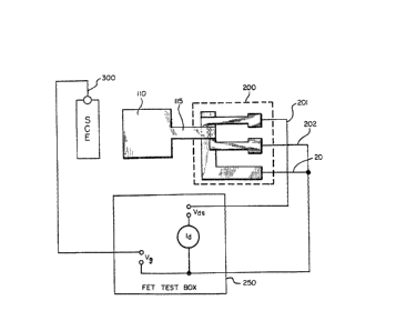
In FIG. 2, a preferred embodiment of a FET
device according to the présent invention is schemati-
cally depicted. In this device a graphite pad 110 con-
nects a sensing area to gate 115 of FET 200. FET 200
may thus be placed away from the well in which the
analyte is placed or even on the reverse surface of the
substrate by connecting a ~ET test box to source lead
201, drain lead 202 and bulk lead 203 of FET 200 and to
2~ a standard calomel electrode 300, the device may be used
as an i~n-selecti~e electrode
~ The Vds of a FET test box 250 i5 set at a
- constant value of approximately 2 volts. The ~d is
fixed at a value of -50 microamps. The frit of elec-
trode 300 and the membrane area over the graphite are
completely immersed into a test solution. The gate
voltage is read in millivolts. As the concentration of
an ion changes, the potential of the membrane changes
according to the Nernst equation. The FET box is confi-
gured to adjust the Vg (gate voltage) proportionally to
the membrane potential change, such that a constant Id
~LX8~
-- 11 --
is maintained. This Vg adjustment is used in the Nernst
equation as the negative equivalent of membrane
pote~tial.
The membranes useful in sensing element and
FET embodiments of the present invention may be prepared
as follows:
For the sensing element embodiments (i.e.
those not having an active device mounted on the first
surface) a pH membrane may be prepared by dissolving:
20 mg tridodecylamine (ionophore), 132 mg dibutyl seba-
cate (plasticizer), 51 my polyvinyl (PVC) and 1.4 mg
sodium tetraphenylboron in 1 ml tetraphydrofuran (TH~).
A potassium membrane may be prepared by dis-
solving 2.0 mg valinomylin ~ionophore), 140 mg di-2-
ethylhexyl adipate ~plasticizer) and 60 mg PVC in 1 ml
THF.
A sodium memhrane may be prepared by preparing
a stock PVC/THF solution of 33.0 mg PVC in 1 ml THF and
~20 dissolving 41.8 mg o-nitrophenyl octylether (plastic-
;izer), 1.0 mg sodium tetraphenylboron, and 4.7 mg monen-
sin methylester (ionophore) in 0.2 ml of the stock PVC/-
THF sslution.
For both sensing element embodiments and for
FET embodiments (i.e. those having an active device
mounted on the first surface), a calcium membrane may be
prepared using a stock PVC/THF solution of 13.2 mg PVC
in 0.4 ml THF and dissolving 41.8 mg o-nitrophenyl
octylether, 0.47 mg sodium tetraphenylboron and 4.7 mg
3Q Fluka. #21192 calcium ionophore in 0.2 m~ of the stock
PVC/THF solution.
For F~T embodiments, a potassium membrane may
be prepared by dissolving 41.8 mg o-nltrophenyl octyl-
ether, 0.47 mg sodium tetraphenylboron and 4.7 mg vali-
nomycin in 0.2 ml of the same stock PVC/THF solution
~282~L~8
- 12 ~
described for the calcium membrane.
Materials useful in the construction of ion-
selective electrodes as described herein may be obtained
from the following sources. PVC from Polysciences In-
corporated, Warrington, Pennsylvania; THF from Aldrich
Chemical Company, Milwaukee, Wisconsin,, sodium tetra-
phenylboron from Aldrich Chemical Compan~, Milwaukee,
Wisconsin; dibutyl sebacate from Kodak Chemicals,
Rochester, New York; tridodecylamine from Kodak
Chemicals, Rochester, New York; valinomycin from Sigma
Chemical Company, St. Louis, Missouri; di-2-ethylhexyla-
dipate ~rom Polysciences, $nc., Warrington,
Pennsylvania; o-nitrophenyloctylether fr~m Fluka
Chemical Corporation, Ronkonkona, New York; monensin
methyl ester from Calbiochem Biochemicals, San Diego,
California and Calcium Ionophore #21192, Fluka Chemical
Corp., E~onkonkona, New York.
A useful substrate material for embodiments of
the present invention is a thermoplastic polyester resin
for injection molding available from General Electric
Corporation, Albany, New York, as the product Valox~
865. Screens for screen printing according to the pre-
sent inventor may be obtained from Microcircuit En-
gineering Corporation Mount Ho~ly, ~ew Jersey as 200MES~W/1.655 wire @ 30 degree an~le using type ES emulsion.
A graphite ink use~ul according to the present invention
is available from Acheson Colloids Company, Port Huron,
Michigan as product #423SS.
30In one embodiment of the present invention the
ion~selective electrode, as illustrated in FIG. 3, a
plastic substrate 700 holds five electrical pins (701,
702, 703, 704 and 705), a reference electrode 710, five
ion-selective-electrode membranes (751, 752, 753, 754
35and 755), a first insulating layer 730 have apertures
defining respective spaces 740 for reference electrode
4~3
- 13 -
710 and 741 745 respectively for sensing electrodes 721-
725, cylindrical apertures 731-736 pass through sub-
strate 700, and conductors (7?1-726) between the pins
(701-706) and the reference electrode and the
membranes. Reference electrode 710 is a small silver/-
silver chloride square. It is inse~ted in the bottom of
substrate 700 with a potassium chloride gel above it.
The gel is exposed to the test solutions via a small
0.005 inch diameter hole in the top surface of substrate
700-
Deposited above layer 730, overlapping the
respective perimeters oE spaces 741-745 are square
membrane anchors 761, 762, 763, 764 and 765, each of
- which has a central, square aperture respectively
beneath membranes 751-75~. A second insulating layer
760 is approximately identical to layer 730 in
configuration, including the location and size of
apertures 741-745, but lies above membrane anchors 761-
765.
; 20
The top side of substrate 700 is covered with
conductive car~on traces from the pins to the area where
the ion-selective-electrode membranes are placed. An
insulating pattern is formed over the conductive traces
to protect them. The ion-selective electrode membranes
721-723 are placed above the insulating and conductive
traces.
Moreover, although a single membrane anchor
layer has been described herein, it is contemplated that
a plurality of membrane anchor layers may be intersolu-
bilized with the ion-sensitive membrane and interleaved
with insulating layers to provide as circuitous a path
for moisture to reach any metallization as may be prac-
tical or desired.
Furthermore, in addition to those materials
listed herein, thermoset materials suitable for tight
~1.2~32~iia
- 14 -
adherence to a substrate and for insulating layers in-
clude, for example, epoxies, urethanes, phenolics, ~nd
silicones-. In addition to the thermoplastic material
employed herein, the following thermoplastic materials,
for example, may be useful for intersolubilization with
ion~sensitive membranes, e.g., P~C, PVAc, PVAl, cellu-
losics, acrylics, urethanes, PVDF, and polyesters. In
general, anchor materials which are soluble in the same
solvent or the membrane may be.intersolubilized with the
membrane. Exceptions to this general rule involve ma-
terials which may not be intersolubilized because of
mismatch in crystallinity, packing, or interaction para-
meters as defined by, for example: ~lory, "Principles
of Polymer Chemistry," Cornell ~niversity Press, Ithaca,
15 ~ew York, (1953) ~u~gLns, Polym. J. ~ 4, 51l ~19733
Hildebrand, Ind. Eng. Chem. Fund., 17, 365 (1978); and
Hansen, J. Paint Technol., 39, 511 (1967).
Therefore, it is intended that the present
- invention include all such variations and improvements
which come within the scope oE the invention as claimed.
~ ~ 30
:~
,