Note: Descriptions are shown in the official language in which they were submitted.
1~8246~
BACKGROUND OF T~E INVENTION
The present invention yenerally relates to
phase-locked oscillators, par~icularly ~o a phase-locked
oscillator employing a phase-locked loop, and more
S particularly to a phase-locked oscillator employing a
phas.e-locked loop, which is suitabl~ for applications
requiring conservation of ele~tric power, such as in a
portable radio receiver/transmitter, and the like, and in
which the phase-locked loop is intermittently operated.
1~ Among means for ~a~ing a~erage el~tric power
consumption on radio receiver/transmitter, especially
on portable radio recei~er/~ransmit~er, means of inter-
mittently operating part of circui~s of phase-locked
oscillators requiring relatively large electric power
have been d scribed in Japanese Patent Unexamined
P~blication Nosc 58-66434 and 58-159029. Generally,
such a phase loc~ed oscillator comprises a reference
oscillator, a reference frequenoy aivider for dividing the .
frequency o~ output clock~ of the reference oscillator,
a voltage-controlled oscillator ~hereinaftsr abbreviated
~o "VCO"), a frequency ~ivider for dividing the frequency
of the output clocks of the VCO, a phase comparator for
comparison in phase between the frequency-division carry-
signals of the frequency dividers, and a loop filter for
smoothing the output error signal of the phase comparator
-- 1 --
.,
Z~
1 and for feeding a VCO control voltage. In the above-
mentioned prior art references, the average electric
power consumption saving is attained by wholely or
partially interrupting the electric power supply for the
circuits except the VCO. In this case, a voltage-hold
circuit for holding a control voltage ~v be applied to
the VCO (that is, the output of the loop filter) to a
value just before the cut-of of the e}ectric power
supply is provided to keep the output frequency of the
VCO constant during ~he cutting-off of the electric
power supply.
HowPver, no co~sideration has heen given~O the fact
that the two output signals of the reference frequency
divider and the frequency divider to be ed to the phase
comparator should be made to be in phase whenever the
electric power supply is ~pplied again from its off-
state.
Each of the ræference fre~uency divider a~d the
freque~cy divider generally includes a counter consti~
tuted by one or more bistable trigger ci~cuits or flip-
flops. The number of internal states in a binary
counter constituted by a plurality of flip-flops, n in
number, is 2 , and the i~ternal state of the counter at
the time of turning on of the electric power supply is
indefinite. In other words, the number of input clock
sign~ls in a period from the turning on of the electric
power supply to the output of the first carry is within
a range of 2n but indefinite whenever the electric power
~ ~ ~Z ~6~
1 supply is turned on. The electric power supply is cut
off by an intermittent operation from -the phase-locked
state. For this reason, the probability that the
respective si~nals fed to th~ phase comparator at the
time of turning on of the electric power supply will become
in phase is very little even if the output fr~quency of
the VCO does not change during the of:E-state of the
ele~tric power supply, so ~hat, in general, a phase
difference occurs between the signals. Because the
phase difference after turning on of the elPctric power .
supply produces a large error signal to be applied to
the VCO through the loop ~ilter, the ~reque~cy of the
VCO is temporarily widely changed. Thereafter the
~requency of the VCO is returned ~o a locked state by a
yeneral pull-in effect. The use of such an int~rmittently
operative phase-loc~ed oscillator as an oscillator ~or
a receiver o~ a radio receiver/transmitter causes a
problem ~n that unr~ceivable conditions temporarily occur
because of the shifting of the fre~uency of the VCO every
20 time the alertric power supply is turned on in the:inter-
mittent operation.
SUMMARY OF T~E INVENTION
An object of the present invention is to provide
a phase-locked oscillator arranged to perform an inter-
mittent operation, in which oscillator frequency changeis to be minimized whenever an electric power source is
turned on.
~,
.
8Z ~ ~
1 To attain the above ob~ect, according to the
present invention, counters included in a phase-locked
~ loop of such a phase-locked oscillator
: are initializéd to a predetermined state to
thereby prevent an erroneous phase-difference signal
from being generated.
In a pxeferred embodiment, to make the timing
for ~he initialization optimum, thexe are newly provided
a zero-phase detect~ng circuit for detecting the fact
that the phase difference between clocks respectively
fed ko a reference ~requency divider and a frequen~y
divider becvmes substa~tially zero to there~y generate
a zero-phase signal~ and a preset puLse generating circuit
for generating a preset pulse signal ~o initialize
both the reference frequency divider and the frequency
divider in synchronism with the zero-phase signal
generated first a~ter the launching of the electric power
: source.
The above-mentioned and other features and
objects of this invention will become more apparent by
reference to the following description taken in connec~ion
with the accompanying drawingsO
BRIEF DESCRIPTION OF THE DRAWINGS
Fig. 1 is a block diagram of an embodiment of
the phase-loc~ed oscillator according to the present
~ invention;
: Fig. 2 is a waveform diagram for explaining the
- 4 -
1~2464
1 operation of the same embodiment;
~igs. 3 and 4 are detailed circuit diagrams
( o~.parts of the same embodiment;
Fig. 5 is a block diagr~n of another embodiment
of the phase-locked oscillator of the invention;
Fig~ 6 is a waveorm diagram for explaining
the operation of the embodimen$ o~ Fig. 5;
; Fig. 7 is a circuit diagram of impoxtant parts
of the embodiment of Fig. 5;
Fig~ 8 is a wa~eform diagram for explaining
the operation of Fig. 7;
Fig. 9 is a diagram o a zero-phase detecting
: circuit depicted in Fig. 5,
Fig. 10 is a block diagram of a further embodi
~' 15 ment of the phase-locked oscillator of the present
invention; and
Figs. llA, llB and 12 are circuit diagrams of
important parts of the embodiment depict d in the block
diagram of Fig. 10.
2 0 I~ESCRIPTION OF THE PREFBRRED EMBODIMENTS
Fig. 1 is a bloc~ diagram showing the arrange-
ment of an embodiment of the phase-locked oscillator of
the present invention.
- Re~erring to Fig. 1, the output of a reference
oscillator 1 is fre~uency-divided into a signal H of
~ a period Tr by a reference frequency divider 2. The
: signal H is fed to one input terminal of a phase comparator
.~, .
~ ~24~i~
1 3. The output of a VCO 5 is frequency-divided into a
signal I of a period Tv by a fre~uency divider 7. The
signal I is fed to the other input terminal of the phase
comparator 3. A phase difference component ~etween the
two signals H and I produced from the phase comparator 3
is fed back to a frequency contxol terminal o the VCO
5 via a loop filter 4 and a voltage-hold circuit 1~. On
the other hand~ an intermittent control signal A
controls a switch 9 to thereby interrupt electric power
10 supply to the circuits 1, 2, 3, 4 and 7 wholely or
partially. In this embodiment the intexmittent control
signal A is fed also to an electric power source launching
detecting circuit 15-1. The output signal of the cir-
cuit 15-1, that is, an initial state setting signal G is
1~ applied to the ~requency dividers 2 and 7.
: The operations o~ the dividers will be now
supplemented. For example, let the frequency dividers 2
and 7 be formed by down-counters, the frequency division
modulus, the ini~ial state, and the carry-pulse output
state of the reference frequency divider 2 are represented
by R, "R", and "1" respectively. The internal s~ate of
the reference frequency divider 2 periodically changes
so as to be "R", "R-l", ..., "2", "1", and "R" succes-
sively as long as electric power is continuously supplied.
Similarly to this, when the frequency division modulus
of the frequency divider 7 is represented by N, the
internal state thereof periodically changes between the
initial state "N" and the carry-pulse output state "1".
-- 6 --
- ` ~ 28;2~64
1 As shown in Fig. 2, when the signal A is at a
"high" level, the switch 9 is closed to thereby energiZe
the circuits. Accordingly, this sta e expresses the
"ON" state of the intermittent operation. When the
signal A is at a "low" level, the switch 9 is opened o
thereby interrupt electric power supply to the circuits.
Accordingly, this state expresses the "OFF" state of
the intermitten~ operation.
In the "ON 1" state of Fig~ 2, the phase-
locked loop of Fig. 1 is in a phase-locked state, the
period Tr between adjacent carry-pulses of the signal
and the period TV between adjacent carry-pulses of the
signal ~ are equal to each other, and the phase relation
therebetween is constant. Next, the operation shi~ts
into the "OFF 1ll state of Fig. 2. It is assumed that
the frequency of the VCO 5 does not change during the
"OFF" state. Next, the signal A turns to a "high" level
and the operation shifts into the "ON 2" state. The
electric power detecting ci~cuit 15-1
makes the initial state setting signal G turn to a
"high" level for a short time in synchronism with the
point in time in which the signal A turns from a 'llow"
level to a "high level", and thereby generates a pulse
~. By the pulse ~, the ~requency dividers 2 and 7 are
simultaneously set to the initial states "R" and "N",
respectivelyO Accordingly, the time Tro or Tvo required
for generating the first carry-pulse on the signal H or
I after the initialization is equal to the period Tr or
-- 7 --
1~8Z~6d~
Tv, and the carry-pulses on the signals H and I are
equal in position to each other.
Although the above description contains an
assurnption that the f requency of the VCO 5 does not
5 change during the "OFF" term, ~he frequ~ncy changes a
little in fact~ In this case, ~he time Tro required ~or
generating the 4irst carry-pulse on the signal H after
the initialization in each of the frequency divide~s by
the pulse ~ is not equal o the time Tvo required for
generating the first carry-pulse on the signal I after the
initialization. The differenc~ therebetween is detectPd
as a phase error by the phase comparator and is fed back
~a the VCO S via the loop ~ilter 4 and the voltage-hold
circuit 10 to thereby correct the ~CO reque~cy.
lS The circuits 15-1, 2 and 7 will be described
in more detail hereunder. The e~ectric power
detee~ing circuit 15-1 is pro~ided to generate
a differential pulse at a level change point of the
intermittent control signal A, that is, at a rise point
of Fig. 2. The circuit 15-1 is constituted by a well-
known circuit, such as a circuit using gate delay~ a
clock differentiating circuit having two D-type flip-flops
casc~de-connected, or the like.
Fig. 3 shows an embodiment of the frequency
divider 7 (or the reference frequency divider 2). This
differs from a general fre~uency divider in that an OR
gate 34 is additionally provided to receive the initial
state setting signal G from outside. When a clock CL is
~ 8 --
, .
.
1~3246~
1 fed to a coun~er 31 the state of which is monitored by
- a carry detecting circuit 32, a carry-pulse CR is
generated under the carry-state. The carry-pulse CR
drives an initial s~ate se~ing circuit 33 via the OR
S gate 34 so that the coun~er 31 is initialized. Similarly
to this, the counter 31 is initialized by ~he initial
state setting signal G regardless of the state of the
cou~ter at that tim~.
Fig. 4 shows ano~her embodime~t of the frequency
divider 7. In ~he case where the re~uency of the VCO 5
i5 high, it is necessary that the frequency divider 7 is
constituted by a high-speed pre-scaler 6-l and a low-
speed frequency divider 6-20 In this embodiment, each
of the high-speed pre~scaler 6-l and the low-speed
frequency divider 6-2 employs the same circuit arrange-
ment as shown in Fig. 3, so that initialization can be
made externally. The carry-output CR-O of the high-
speed pre-scaler 6-l is fed to the low-speed frequency
divider 6-2 as a clock for the latter.
Although the embodiment of Fig. 1 shows the
case where the change point of the intermittent control
signal is detected by the electric power
detecting circuit 15-1, the invention is not limited to
- this embodiment, but applicable ~o the case where the
output of the switch 9, that is, ~he on/off state of
the electric power source, is detected as another embodi-
ment.
Even if either the reference frequency divider
_ g _
- -: ' ~ - - - - ~ -
~ 8~
1 2 or ~he frequency divider 7 in the embodiment of Fig. 1
is intermittently operated, it is necessary to initialize
both the two frequency dividers at the time of launching
the electric power supply. However, if the phase error
between the two signals fed to the phase compar~tor
after the turning on of electric.Power supply is permitted
wi~hin a certain limit, it is not necessary to initialize
all of the counters in the two frequency dividers at the
time of turning on of the electric power supply. In particu-
lar, it is not necessary to initialize lower signi~icantbits of the counters in the two frequency dividers, while
the other, more significant bits o ~he counters should
~ be initialized.
- Other embodiments effectiv~ly applied to the
case where the frequency of the reference oscillator
differs rom the fxequency of ~he VCO or in other words
where the instantaneous phase di~ference between the two
oscillators changes every moment, will be described
hereunder. More in detail, the embodiments are arran-
ged to detect the point in time when the phase differencebetween clock signals respectively fed to the reference
frequency divider and the frequency divider becomes
minimized ~preferably zero) for the purpose of minimizing
the phase diference between two signals applied to the
respective inputs of the pha~e comparator after the
turning on of the electric power supply in an intermittent
operation or in other words for the purpose of minimizing
the phase difference between two signals generated from
-- 10 --
.~.
~X8~i4
1 the frequency dividers, and thereby initialize the two
frequency dividers at that point in time.
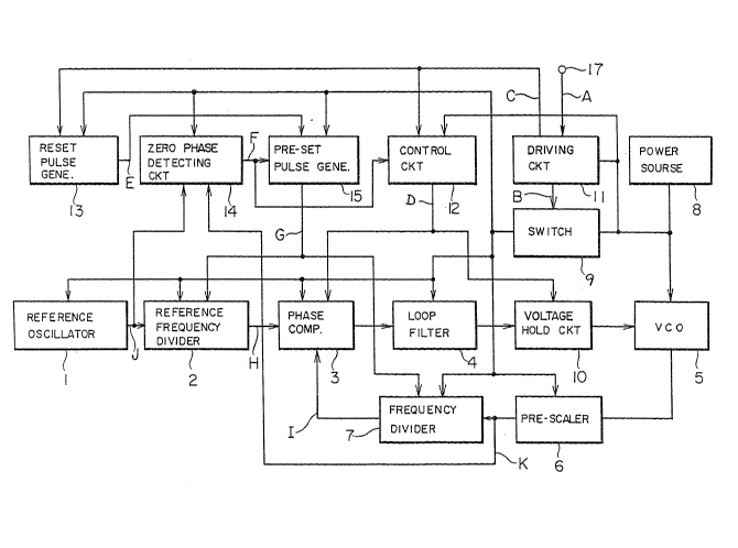
Fig. 5 is a block diagram showing the arrange-
ment of another embodiment of the phase-locked oscillator
according to the invention.
In Fig. 5, a clock signal J generated from a
reference oscilla~or l is fed to a referenc~ frequency
divider 2, and a frequency-division carry-signal ~ of
the reference frequency divider 2 is fed to one input
terminàl of a phase comparator 3. On the other hand, a
clock signal generated from a voltage-controlled oscilla~or
(~CO) 5 is fed to a pre scaler 6, and an output clock
signal K o the pre-scalex 6 is ed to a ~requency diviaer
7. ~ requen~y-division carry-signal I of the frequency
di~ider 7 is fed to the other input tenminal of the phase
comparator 3, and a phase error signal generated ~rom the
phase comparator 3 is smoothed by a 1QP filter 4. The
smoothed phase error signal is applied to a frequency-
control terminal of the VCO S via a voltage-hold circuit
10 to perform an intermit~ent operation. The phase-locked
oscillator of this embodiment is constituted by the
above-mentioned circuit elements. Circuit elements 9
and 11 to 15 which will be described later and the
circuit 10 is additionally provided for the intermittent
operation. An intermittent operation control signal A
fed through a terminal 17 is converted into a signal B
through a driving circuit ll, so that the signal B
drives a switch 9 to interrupt a voltage and a current
~ 8Z ~ ~
1 fed from a power source 8. Another signal C generated
frQm the driving circuit 11 is fed to both a co~trol
cir~uit 12 and a reset pulse generating circuit 13 which
in turn supplies a reset pulse signal E to a preset
pulse generating circui. 15 at the time of ~urning on of th0
elec~ric power supply. A zero-phase de~ec~ing circuit 14
receives the clock signals J and K and supplies a zero-
phase signal F to both the preset pulse generating
cirsuit 15 and the control cirouit 12. The preset
10 pulse generating circuit 15 de~ects the zero-phase signal
F fed first_ after the turning on of the ele~tric power
supply, and generates a preset-pulse signal G to be
applied to both the ~efe~ence frequency divider 2 and
the frequency divider 7. A signal D generated from the
control circuit 12 controls interruption/passa~e of the
signals H and I ed to the phase comparator 3 as well
as cvntrols the sta~e of voltage-holding/current-conduction
ffl the voltage-hold circui~ 10. In thi~ embodiment, the
VCO 5, the switch 9, the d~iving circuit 11, and the
control circuit 12 are supplied with a voltage directly
from the electric power source 8, and the other circuits
are energi2ed with an intermittent voltage through the
switch 9.
The operation of ~he embodimen~ of ~ig. 5 will
be described by reference to ~he wavefonm diagram of
Fig. 6. Let the intermittent operation be in an "ON"
state when the intermittent control signal A is at a
"high" level or let ~he intermittent operation be in an
- 12 -
,,
1~8'~46~
1 "OFF" state when the signal A is at a "low" level. The
driving circuit 11 generates the signal B obtained by
delaying the falling point of the signal ~ by a CQrtain
amount of time T 1~ and the signal C obtained by delaying
the rising point of the signal A by a certain amount of
time T 2~ The control circuit 12 turns the signal D to
a "low" level in response to ~he falling of the sig~al
C to thereby temporarily hold the output voltage of th~
loop filter 4 in the ~oltage-hold circuit 10. Taking
into consideration the r~sponse time re~uired for the
voltage-hold operation, the time for interrupting the
electric power source by the switch 9 is delayed by the
amount of tLme ~1 compared with the falling point of
the signal A. ~hile the intermit~ent operation is in
the "ON 1" sta~e of Fig. 6, the phase-locked oscillator
is i~ the phase-locked sta~e and, accordingly, the signals
H and I are in phase with each other. Next, when the
intermittent operation turns to the "OFF 1" state, the
~requen~y of the VCO 5 is kept constant owing to the
operation of the voltage-hold circuit 10. Next, when
the intexmittent operation turns to the "ON 2" state,
the signal B rises in synchronism with the rising of
the signal A to there~y turn on the switch 9 to energize
each of the circuits. Taking into consideration the
response time in each of the circuits after the t.urning-on
of the electric power source, the rising point of the
signal C is delayed by the amount of time l2 compared
with the falling point of the signal B. In order to
28Z~4
1 r~m~ve disused frequency-division carry-signals generated
from the reference frequency divider 2 and ~he frequency
divider 7 just aIt.er the turning on of the electric
power source, the signals H and I are gated at the
s input stage of the phase ~omparator 3 by the signal D
wi~h the "low" level. The reset pulse ge~erati~g circuit
13 detects the rising of the signal C to thereby generate
a r~set pulse ER for the signal E. Thereby, the preset
pulse generating circuit 15 turns to the sta~e o~ operatio~.
~he operation of the æero-phase detecting circuit 14 will
be described in detail later. Let the clock signals J
- and K be instantaneously subs~antially i~ phase w~e.n ~h~
zero-phase signal F is 3t a "high" level, or let the
clocX signals J and K be out o~ phase when the signal F
is at a ~low'l level. The pr~set pulse generating circuit
15 detects the "high" level of the zero-phase ~ignal F
fed first after the turning on of the electric power
source to thereby generate a preset pulse ~. Because the
reference frequency di~ider 2 and the frequency divider
7 are initialized by the pulse ~, the subsequently
generated frequency division carry-pulses ~C and IC are
substantially in phase. The control circuit 12 makes the
signal D rise to a "high" level in synchronism with ~he
generation of the preset pulse ~. Acsordingly, the
input-stage gate of the phase comparator 3 becomes
conductive to feed tne frequency division pulses ~C and IC
to ~he body of the phase comparator, and, at the same
tlme~ the voltage-hole circuit 10 changes to a non-nold state
- ~4 -
324~;4
to receive a new voltage frc~m the loop fil~-er 4. There-
after, the phase-locked oscillatox performs a general
phase-locked operation. Obring to the operation of the
signal D, ~e input-stage gate of the phase comparator
5 3 blocks disused caxry-signals yenerated rom both the
xeference frequ0ncy divider 2 and the frequen~y ~ivider
7 till the zexo-phase signal turns to a "high" le~el
after the turning on of the electric power source .
It is a matter of course tha~ the reference
frequency divider 2 and the frequency divider 7 used in
th~ embodiment of Fig. S are able to be initialized.
: For 0xample, if the pre-scaler 6 used is able to be
initialized, it is apparen~ ~hat the same operation as
in the embodimen~ of Fig. 1 can be earried c~u~: in the
15 case where the sig~al G i ed into the pxe-scaler and
where the output of the VCO 5 instead of the clock
signal K is ~ed to the zero-phase detecting circuit 14.
If the pre-scaler is not used, the same operation can
be obtained in the case where the VCO ou~put is fed to
the zero-phase detecting circuit.
Fig. 7 shows an embodiment in which the main
circuits of the ~ig. 5 embodime~t are ~ealized by using
more specific circuit elements. ~ig. 8 is a waveform
diagram of the signals at various parts in the embodiment
25 of Fig. 7. Like circuits, signals or waveforms in Figs. 5
to 8 are identified by the same reference characters.
An intermittent control signal A received at a terminal
17 of Fig. 7 is fed to a delay element ll-l of delay time
- 15 -
1~8;Z ~64an OR gate 11-2, a delay element 11-3 of delay time
T2~ and an AND gate 11-4 constituting a driving circuit
11. The output o~ the delay element 11-1 is fed to the
other input terminal o~ the OR gate 11-2. The output
signal of the OR gate 11-2 is shown as a signal B. The
output of the delay element 11-3 is fed to the other
input ~erminal of the AND gate 11-4. The output signal
of the AND gate 11-4 is shown as a signal C. The delay
time ~1 or T 2 corresponds to ~he amount of time ll or
l2 shown in Fig. 6. The signal B drives a switch 9 to
open/close the path between input/output terminals 18
and 19. The control circuit 12 is constituted by a
falling differential pulse generating part having a
delay inverter 12-1 and a two-input NOR gate 12-2, and
an R-S flip-flop part having two-input NOR gates 12-3
and 12-4. The signal C is ed to both the delay inverter
12-1 and the NOR gate 12-2, and the output of the latter
is fed to the NOP~ gate 12-3. When the signal C falls,
the output signal D of the NOR gate 12-3 turns to a
"low" level. The voltage-hold circuit 10 is constituted
by a switch 10-1 for open/close the path between an
input terminal 20 and an outpu~ terminal 21, and a
capacitor 10-2 holding a contxol voltage provided at
the output terminal side. When the signal D falls, the
switch 10-1 turns to an open state. Accordingly, the
voltage having been impressed on the terminal 20 by the
loop filter just before the falling point of the signal
D is held by the capacitor 10-2 and is applied to the
- 16 -
2 4~
1 VCO 5 through the ~erminal 21. The phase comparator 3
is constituted by a comparator body 3-1 and two-input
AND gates 3-2 and 3-3. A signal H fed from a terminal
22 and the signal D are fed to the gate 3-2, and a signal
I fed from a terminal 23 and the signal D are fed to
the gate 3-3. The respective phases of the outpu~
signals of the two gates 3-2 and 3-3 are comparea with
each other, and, as the result, an error signal is fed
to the loop filter 4 from a ~erminal 24. The reset
! 10 pulse generating circuit 13 is constituted by a delay
inverter 13-1 and a two-input AND gate 13-2 and generates
a reset pulse ER for a signal E in synchronism with the
rising of the signal C. The zero-phase detecting circuit
14 is constituted by a phase comparing part 16 surrounded
by the two-dotted chain lines of Fig. 7 and a pulse
width discriminating part provided to the rear stage
thereof. In the phase comparing part 16, a circuit
constituted by NOR gates 14-1 to 14-9 is commonly known
as a phase/frequency comparator, and therefore, detailed
description of the operation thereof will be omitted. In
this embodiment, in order to eliminate a frequency
discriminating function from a phase/~requency comparator,
clock signals J and K are fed to four-input NOR gates
14-2 and 14-4 through inverters 14-10 and 14-11, respec-
tively. As the result, a pulse signal corresponding tothe instantaneous phase difference between the clock
signals J and R fed to terminals 25 and 26 is generated
from a gate 14-12 through the gate 14-2 or 14-4. The
- 17 -
,; . :
-- ~x~3x~
1 pulse width discriminating part is constituted by a D-
type flip-flop 14-16, a data gate (constituted by a delay
element 14-13 and a two-input NAND gate 14-14~, and a
clocX gate 14-15. The flip-flop 14-16 is of such a
type that a data signal fed to a term.inal D is ~rans-
mitted to a terminal Q with ~he rising of a clock
signal fed to a terminal C and that the output of the
terminal Q is reset when a signal app:Lied to a terminal
R is at a "high" level. In this embodiment, the signal
E is applied to the terminal R to thereby keep the output
of the terminal Q at a "low" level at the time of turning
on of the electric power source to tner~by prevent the
malfunctio~ thereo~. The output signal L of the two input
OR ga~e 14-12 receiving ~he output si~nals o the gates
14-2 and 14-4 is ed to both the delay eleme~t 14-13 and
the two-input NAND gate 14-14, th~ output of the former
being fed to the latter. The output signal M of the gate
14-14 is fed to the terminal D of the flip-flop 14-16.
The output signal N of the two-input NAND gate 14-15
receiving the output signals of the gates 14-6 and 14-8
is fed to the terminal C of the flip-flop 14-16. Because
the rising par~ o~ the signal L is scraped off for a
delay time 13 by the delay element 14-13, a corresponding
part o~ the signal M is kept at a "high" level in the
case where the pulse width of the signal L is less than
the time T3. The signal M after the discrimination of
pulse width is sampled by the signal N and is held in
the flip-flop 14-16. The output signal F from the terminal
- 18 -
~, .
_ ~ 46
1 Q of the flip-flop 14~16 is fed to the gate 12-4 to
thereby make the signal D rise to thereby make the
switch 10-1 tur~ o~. In the preset pulse generating
circuit 15, a function of detecting the "high" level of
the signal F appearing first after the .~urning on of the
electric power source is attained by bo~h a D-~yp~ flip-
flop 15-1 and a two-inpu~ ~ND gate 15-2. The flip-flop
15-1 is of the same type as the flip-flop 14-16. The
output from a terminal Q of the flip-:Elop 15-1 is fed to
both a terminal D thereof and the gate 15-2~ A terminal
C of the flip-flop receives the output of the gate 15-2,
and a ~enminal R receives the signal E. The other input
terminal of the gate 15-2 receives the signal F. When
the electric power source is turned on, both the signal F
and the output signal O from a terminal Q of the flip-flop
15~1 turn to a "low" leveL and the output from the
terminal Q turns to a "high" le~el. Accordingly, the
gate 15-2 is opened for the signal F. With the rising
of the signal F~ the signal O turns to a "high" level
and the output from the terminal Q turns to a "low"
level to thereby m~ke the gate 15-2 closed for the
signal F. The above-described function can be made by
a general R-S flip-flop using the signals E and F
respectively as a reset signal and a set signal. At the
rising point of the signal O, a preset pulse ~ on a
signal G is generated by a differential circuit consti-
tuted by a delay inverter 15-3 and a two-input AND gate
15-4. The signal G is fed to both the reference frequency
1 9 --
~ ~32464
1 divider 2 and the fre~uency divider 7 through a terminal
27~ Although this embodiment shows the case where the
( signal D is used as a gating signal for the gates 3-2
: and 3-3, ~he invention is applicable, alternatively, to
the case where the signal D is replac~d by the signal O
fed from a terminal 28 in order to use the signal O as
the gating signal.
The operation of the zero-phase detecting
circuit 14 of Fig. 7 will be described hereunder by
reference to the waveform diagram of Fig. 8. In Fig. 8,
let the ra3~io of the frequency of clock J to the frequency
of clock K be 10 to 13~ Accordingly, let the ratio of
the division modulus o~ the re~eren~e ~requency divider
2 to the division modulus of the ~requency di~ider 7
be 10 to 13. When the in~ermittent control signal A
:~ . rises at a point in time t~, the electric power source
is cor~espondingly turn~d on for all of tne circuits and
then the signals F and O are turned *o a "low" level
by the reset pulse ER generated with a delay of time T2.
Thereafter, cloc~ pulses Jl' J2~ etc., are fed to the
terminal 25 and cLock pulses Kl, K~, etc., are fed ~o
the terminal 26, successively. A pulse which corresponds
to ~he phase difference between the clock signals J and
K is generated from the gate 14-2 or 14-4 by the phase
comparing part 16. In the ~rawing, the rising of the
pulse Kl is earlier in phase than the rising of the
pulse Jl and, accordingly, the phase difference pulse
Ll is sent out through the gates 14-2 and 14-12. In
-- ~o --
12~Za~64
l comparison between the next pulses K2 and J2' the falling
of the pulse K2 is earlier than the rising of the pulse
`~ J2 and, accordingly, the pulse L2 is reset at the falling
of the ~ulse K2 by the gate 14-11. The next pulse L3
which corresponds to the difference in rising phase
between the pulses J2 and K3 is sent out through the gates
14-2 and 14-12. The next phase difference pulse L4 is
genera~ed by the pulses J3 and K4~ and successively,
; the phase difference pulse L5 is generated in the same
manner. Corresponding to these operations, clock pulses
Nl, N2, etc., are generated on signal N from the gate
14-15. By the pulse width discriminating function owing
to the delay ~lement 14-13 and the gate 14-14, the
positive pulses on the signal ~ are converted to negative
pulses haviny the width reduced by the time 13. Thus,
; the negative pulses appear on signal M. In the drawing,
a part of the signal M, which corresponds to the pulse
L4, is kept at a "high" level by the pulse width
discriminating function. Accordingly, when the signal
M is sampled by the rising of the signal N, pulses Fl,
F2, etc., on a signal F are obtained as shown in the
drawing. The difference in rising phase between the
clock signals J and K at the rising part of the signal
F is within a range of +~3. In other words, the zero-
phase discrimination error is within a range of +13.
Stric Iy speaking, the zero-phase discrimination error
is slightly larger than ~3 because of the influence of
the data-setup time and data-hold time of the flip-flop
- 21
~C 8~46D~
1 14-16. More strictly speaking, the zero-phase discrimi-
nation error varies corresponding to the timing between
the signals M and N. In oxder to adjust the timing,
a delay element which is not shown in Fig. 7 for the
purpose of simplifying illustration may be provided
to the rear stage of the gate 14-14 or 14-15. By the
rising o the pulse Fl on the signal F, the signals D and
O turn to a "high" level. Thereafter, operations as
described above are carried out.
In the embodiment of Fig. 7, the delay elements
11-1, 11-3 and 14-13 and the delay inverters 12-1, 13-1
and 15-3 are employed as delay means. Those delay means
can be attained by known techniques, such as delay
circuits made up of a combination of resistors and
capacitors, circuits made up of a combination of such a
; combination of xesistors and capacitors and gates, circuits
made by the cascade connection of gates, circuits made
up of gates having the delay time increased, or the like.
Furthermore, it is possible ~hat a signal is partially
delayed by the use of a suitable clock signal as described
later.
In the em~odiment shown in Figs. 5 and 7,
taking into consideration the response time o circuits
as described above, the falling of the signal B and the
rising of the signal C are delayed respectively relative
to the falling of the signal A and the rising thereof.
Accordingly, the effect of the embodiment is that the
intermittent operation can be made without malfunction,
- 22 -
6~
1 or in other words the object of the invention can be
surely attained.
Fig. 9 shows another embodiment of the zero-
phase detecting circuit. The zero-phase detecting
circuit 30 is made up of a phase comparing part
constituted by D-type flip-flops 30-1 and 30-2 and gates
30-3 to 30-8, and a pulse width discrimina~ing part
constituted by gates 30-9 to 30-11 and a D-type flip-
flop 30-12. The D-type fllp-flops are of such a type
that a data signal or an inverted data signal applied
to a terminal D is transmitted directly or invertedly
to a terminal Q or Q, respectively, at the rising time
of a clock signal ed to a terminal C and that the
; output of the tarminal Q is reset to a "low" level when
a signal applied to a terminal R :is at a "high" level.
~he terminals D of the $1ip-flops 30-1 and 3G-2
continuously receive "high" level data signals and the
terminals C of the same receive clock signals J and K
from terminals 30-15 and 30-16, respectively. The output
;
signals of the two terminals Q are fed to both the two-
input NAND gate 30-3 and the two-input NOR gate 30-8, and
the output signal of the two-input NAND gate 30-4 is
applied to the two termina}s R. The output of the two-
input NOR gate 30-5 receiving the clock signals J and K
is fed to the two-input NAND gate 30-7 both directly and
indirectly via the delay inverter 30-6. The output
signals of the gates 3a-3 and 30-7 are fed to the gate
30-4. The output of the gate 30-8 is fed to the two-input
- 23 ~
z~
1 NOR gate 30-10 directly and indirectly via the delay
element 3Q-9. The terminal D of ~he flip-flop 30-12
receives the output of the gate 30-10, and the terminal
C of the same r~ceives the output of the gate 30-3
passing through the delay inverter 30-11. Thus, the
output of the terminal Q, as a zero-phase signal F, is
genarated from a terminal 30-13. A reset signal E from
the reset pulse generating circui~ is applied to the
terminal R of the flip-flop 30-12 to insure the operation
thereof.
The operation of the embodiment of Fig. 9 is
illustrated. The part made up of the flip-flops 30-1
and 30-2 and the gates 30-3 and 30-4 is a known phase/
~ ~requency comparator. A pulse which corresponds to the
- 15 difference in rising phase between the clock signals J
and K is generated from the terminal Q af either one of
the flip-flops. In this embodiment, the gates 30-5 to
30-7 are additionally provided to thereby eliminate the
frequency discriminating function. In other words,
when the difference in rising phase between the clock
signals J and K is larger than a half of the period
of either signal, the flip-flop is reset by the falling
of either signal having risen earlier. This operation
is the same as in the ~ero-phase detecting circuit 14
of F;g. 7.
A further embodiment is shown in Fig. 10.
Fig. 10 is a block diagram of a phase-locked oscillator
positively using the features of CMOS circuits, and
- 24 -
~Lz~3za~64
1 Figs. llA, llB and 12 are diagrams showing part of the
same in detail. An essential difference between the
~ embodiment of Fig. 10 and the embodiment of Figs. 5 and
- 7 will be now described. Of the functions of the voltage-
hold circuit 10 shown in Figs. 5 and 7, the sampling
function is assigned to a phase comparat~r as described
later and ~he voltage-hold func~ion is assig~ed to a
capacitor included in a loop filter 4. Accordingly,
the voltage-hold circuit 10 shown in Figs. 5 and 7 is
removed and is not shown in Fig. 10. Although Fig. 5
shows the case where the output of the VC0 5 is divided
by the combination of the pre-scaler 6 and the frequency
divider 7, Fig. 10 shows the case where a two-modulus
pre-scaler capable of selecting one from two frequency
divi~ion ~oduli corresponding to the external signal is
used as a pre-scaler 48 and where tha output of the VCO
5 is divided by the combination of the pre-scaler 48, a
main frequency divider 45 and a swallow frequency
divider 46. The intermittent control circuit 42 of
Fi~. 10 represents several circuits lumped under one name
or in other words the circuit 42 is a multifunctional
circuit which is equivalent to all ~f the dri~ing circuit
11, the control circuit 12, the reset pulse generating
circuit 13, the zero-phase detecting circuit 14 and
the preset pulse generating circuit 15 of Fig. 5. In
Fig. 10, the part 40 surrounded by dotted chain lines,
including the reference frequency divider 2, the phase
comparator 41, an intermittent control circuit 42, a
3Z4~i4
l main frequency divider 45 and a swallow frequency
divider 46 and further including bu~fers (I and II) 43
and 44 and a modulating cixcuit 47, is attained hy CMOS
circuits, ~or example, a CMOS custom integrated circuit.
As commonly known, a C~OS circuit is characterized in
that a current except a leak current does not occur as
long as an input signal i5 fixed at a "low" level or
a "high" level and in that an output signal of the
static CMOS circuit is fixed as long as an input signal
is fixed. In order to utilize these characteristics,
a power source voltage is continuously impressed on a
terminal 49 of the part 4a surxounded by the dottecl
chain lines, and the buffers 43 and 44 are respectively
interposed between the reference osci~lator l and the
reference frequency divider 2 and between the two-modulus
pre-scaler 48 and the main and swallow frequency divider
45 and 46. The intermittent operation is performed by
interruption of a signal input to the buffers so that
average electric power consumption is reduced. Generally
a feedback signal is fed back from a swallow frequency
divider ~o a two-modulus pre-scaler. ~he modulating
circuit 47 inserted in the eedback path from the swallow
frequency divider 46 to the two-modulus pre-scaler 48 as
described later is used in this embodiment to thereby
make the intermittent operation more securely.
Various parts will be now described by reference
to the drawings, in which signals having the same function
in Figs. 5, 7, 10, }lA, llB and 12 are identiied by the
- 26 -
1~8~a~6~
1 same reference character. Embodiments of the buffer43 or 44 are shown in Figs. llA and llB. In the drawings,
a clock signal J lor K) is ed to a terminal 51, an
intermittent signal C is fed to a terminal 52, and an
output clock signal J' Ior K') is fed to both the
reference frequency divider 2 ~or main and swallow
fre~uency dividers 45 and 46) and the intermittent
control circuit 42. In the e~bodiment of Fig. llA, the
signals J ~or K~ and C are fed to a two-input NAND gate
54, and the output of the later is connected to the
terminal 53. When the intermittent signal C is at a
"high'l level, the output signal J' ~or K') of the NAND
gate 53 is generated as an inverted signal o~ the signal
J (or K). When the intermittent signal C is at a
"low" level, the output of the NAND gate 53 is fixed at
a "high" level. In the ambodiment of Fig. llB, PMOS
transistors 57-2 and 57-3 and NMOS transistors 57-4 and
57-5 are seria~ly connected in order between terminals
55 and 56, an NMOS transistor 57-6 is connected between
the junction point between the transistors 57-3 and 57-4
and the terminal 56, the junction point beiny connected
to a terminal 53. The respec~ive gates o the transistors
: 57-2 and 57-5 are connected to the terminal 51, the
gate of the transistor 57-4 is directly connected to the
texminal 52, and the gates of the transistors 57-3 and
57-6 are connected to the terminal through an inverter
: 57-1. A feedback resistor 57-7 is inserted between the
terminals 51 and 53. Generally, the terminal 55 is supplied
:
- 27 -
~X~Z~64
1 with a positive electric source voltage and the terminal
56 is grounded. In this embodiment, when the inter-
mittent signal C, applied to the terminal 52 i5 at a
"high" level, the transistors 57-3 and 57-4 are co~ductive
and the transistor 57-6 is non-conductive. Accordingly,
the signal J ~or K) applied to the terminal 51 is
amplified and inverted and the inverted signal is sent
out from the terminal 53. When the signal C is at a "low"
level, the transistors 57-3 and 57-4 are non-conductive
and the transistor 57-6 is conductive. Accordingly, the
output is fix~d at a "low" level.
The intermittent signal C is formed from the
intermittent control signal A as described later. In the
embodiment of Fig. llA, when the signal C is at a "low"
level, any electric current except a leak current flowing
in the transistors ~orming the gate does not flow. In
the embodiment of Fig. llB, when the signal C is at a
; "low" level, any electric current except a leak current
flowing in the transistors and resistor 57-7 does not
flow. Furthermore, in both the embodiments, when the
signal C is at a "low" level, the output level is fixed
at either a "high" or a "low" level. Accordingly, any
electric current except a leak current is not consumed
in circuits connected to the rear s~age of the respective
buffer. Thus, the intermittent operation for the part
40 surrounded by the dotted chain lines can be equivalently
made with keeping the application of a power source voltage
to the terminal 49.
- 28 -
. . ~
~ 82 ~
1 Fig. 12 shows a further embodiment. In the
drawing, a driving cixcuit 60, a reset pulse generating
circuit 61, a zero-phase detecting circuit 62 and a preset
pulse generating circuit 63 correspond to the intermittent
control circuit of Fig. 10. The reference numerals 60-4,
61~1t 61-2, 62-16, 63-1, 63-2, 63-3 and 47-1 respectively
designate D-type 1ip-1Ops for transmitting the data
signal from the terminal D to the terminal Q at the rising
o the clock signal fed to the terminal C. Of these,
the flip-flops having the terminal R are arranged so that
the terminal Q is reset to a "low" level when the signal
applied thereto turns to a "high" level.
In the driving circuit 60, an intermittent
signal A from a terminal 65 passes ~hrough an integra~ed
circuit constituted by a resistor 60-1 and a capacitor
62-2 and is fed to ~oth a two-input AND gate 60-3 and
a two-input NOR gate 60-5. The terminal D of the flip-
flop 60-4 is connected to the output of the gate 60-3,
; the terminal C is connected to the output of a gate
41-12 of a phase comparator 41, the terminal Q is
connected to the input of a gate 60-6, and the terminal
Q is connected to the input of the gate 60-5. The output
of the gate 60-3 is connected to the other input terminal
of the two-input NAND gate 60-6, and the output signal
C of the gate 60-6 is applied to the buffers 43 and 44
of Fig. lQ through a terminal 67. The output signal B
of the gate 6Q-5 is applied to the switch 9 of Fig. 10
through a terminal 66.
- 29 -
~8~64
1 In the reset pulse generating circuit 61, the
first flip-flop 61-1 and the second flip-flop 61-2 are
wired in a cascade connection. The first D terminal
receives the signal C, the first Q terminal is connected
to the second D terminal, and the first and second C
terminals receive the signal J' from a terminal 6B. The
first and second Q terminals are connected to a two-input
NAND gate 61-3, the output of the gate 61-3 ~eing a
reset signal E.
In the zero-phase detecting circuit 62, a
circuit constituted by gates 62-1 to 62-15 and a flip-
flop 62-16 is fundamentally equivalent to the zero-
phase detecting circuit 14 of Fig. 3. In this embodimen~,
the signals Ji and K' fed from the terminals 68 and 69
to ~e compared in zero-phase are respectively fed through
gates 62-18 and 62-19 to the gates 62-1, 62-10 and
62-3, 62-11. The Q-terminal signal of a flip-flop 63-1
in the preset pulse genera~ing circuit 63 is fed to
the other input terminal in each of the two-input NAND
gates 62-18 and 62-19. The signal F and the inverted
signal F axe generated from the terminals Q and Q of the
flip-flop 62-16, and the signal E from the reset pulse
generating circuit 61 is fed to the terminal R.
In the preset pulse generating circuit 63, the
signal F fed to the terminals D of flip-flops 63-1 to
63-3 is respectively sampled by the output signal of the
gate 62-15, the signal K', and the signal J'. The Q-
terminal signal O of the flip-flop 63-1 is fed to two
- 30 -
~X82464
1 gates 41-10 and 41-11 in the phase comparator 41, and
the Q-terminal signal is fed to the gates 62-18 and
62-19. Both the Q-terminal signal of the flip-flop 63-2
and the signal F are fed to a ~wo-input NOR gate 63-4,
and the output signal G2 of the gate 63-4 is supplied
through a terminal 71 to both the main frequency divider
45 and the swallow frequency divider 46 of Fig. 10~
Both the Q-terminal signal of the flip-flop 63-3 and the
signal F are fed to a two-input NOR gate 63 5, and the
output signal Gl of ~he gate 63-5 is supplied through
a terminal 70 to the reference frequency divider 2 of
Fig. 10. The signal E is applied to the respective
terminals R of the flip-flops 63-1 to 63-3.
In the phase comparator 41, a phase comparing
circuit constituted by gates 41-1 to 41-9 is arranged
in such a manner as disclosed in U.S. Patent 3,610,954.
~he signals ~ and I fed from terminals 72 and 73 to be
compared in phase are respec~ively passed through two-
input NAND gates 41-10 and 41-11 and fed to the gates
41-1 and 41 3. The output of the gate 41-2 is applied
to the gate of a transistor 41-14 through an in~erter
41-13, and the output of the gate 41-4 is applied to the
gate o a transistor 41-15. The PMOS transistor 41-14
and the NMOS transistor 41-15 are serially connected
between terminals 75 and 76 to thereby form a so-called
charge-pump circuit. The signal at the junction point
between the two transistors 41-14 and 41-15 is fed
through a terminal 74 to ~he loop filter 4 of Fig. lQ.
- 31 -
~2~ 64
1 The terminal 75 is energized with ~he same voltage as
the terminal 49 of Fig. 10, and the terminal 76 is
( generally grounded. ~he output signal o a two-input
NOR gate 41-12 receiving the output signals from the
~ates 41-6 and 41-8 is fed to the terminal C of the
flip-flop 6~-4.
In the modulating circuit 47, ~he signal H
from a terminal 77 ~that i5~ the output signal from the
reference ~requency divider 2 of Fig. 10) is applied
to the terminal C of a flip flop 47-1, the Q-terminal
signal is fed back to the terminal D, and the signal F
is applied to the terminal R. Both the Q-kerminal
signal and the signal P from a terminal 78 (that ~, the
output signal from the swallow frequency divider 46 of
Fig. 10) are fed to an exclusivP OR ~EX-OR) gate 47-2,
and the output signal of the gate 47~2 is fed through
a termina} 79 to the pre-scaler 48 of Fig. 10.
The operation of the embodiment shown in
Figs. 10 to 12 will be described hereunder. For the
convenience of description, the t~chnique of Fig. llB
is applied to each o~ the buf~ers 43 and 44. Because
the operation of the embodiment shown in Figs. 10 to
12 i~ fundamentally equal to that of the embodiment
shown in Figs. 5 and 7, description will be made with
Z5 reference to the waveform diagrams of Figs. 6 and 8.
First, let the in~ermittent control signal ~ be at a
"high" level to keep the intermittent operation at the
"ON" state. In other words, let the phase-locked
- 32 -
?,
1~3246~
1 oscillator of Fig. 1~ be in the phase-locked state. In
this case, the signals B, C and O are at a "high" level.
Accordingly, a signal which corresponds to the di~ference
in rislng phase between the signals H and I respectively
fed to the terminals 72 and 73 is sent out through the
terminal 74. Furthermore, a signal which rises when
both the signals H and I turn to a "low" level is produced
from the gate 41-12.
Next, the intermittent control signal A turns
to a "low" level. ~owever, the signals C ana B remain
at a "high" level till the clock signal to be fed rom
the gate 41-12 to the flip-flop 60-4 rises. When the
clock signal rises after the terminal 74 turns into the
"high-impedance" state owing to the last phase comparison
lS in the phase comparator 41, the signals B and C turn to
a "low" level. In other words, a little delay exists
between the turning of the intermittent control signal
A to a "low" le~el and the turning of the signals B and
C to a "low" level. The delay is necessary for securely
turning the terminal 74 into the "high-impedance" state.
The delay is equivalent to the difference ll in falling
time between the signals A and B as s~own in FigO 6.
When the signal B turns to a "low" level, the switch 9
of Fig. 10 is opened to thereby interrupt the power
supply to the pre-scaler 4 a . When ~he signal C turns
to a "lowl' level, the output signals J' and K' from the
buffers 43 and 44 are fixed at a "low" level (in the
case of Fig. llB). Accordingly, the output signals H and
- 33 -
:: .. ~...... .
3z4~j~
1 I from the reference frequency divider 2 and the main
frequency divider of Fig. 10 remain at a "low" level,
and the terminal 74 is kept in the "high-impedance"
state. At this time, the VCO 5 is caused to freely
oscillate with a regular frequency by the voltage held
in the loop filter 4. The merit of the above-mentioned
procedure for turning the intermittent operation into the
"OFF" state exists in that the signal which corresponds
to the difference in rising phase between the signals
E and I at first after the returning into the "ON" state,
can be generated without malfunction. Furthermore,
when the signals A, B and C are at a "low" level, the
circuit 40 and the pre-scaler 48 o Fig. 10 are in a
state of ~o electric power consumption.
Next, when the intermittent control signal A
returns to a "high" level, the signal B immediately turns
to a "high" level to thereby restart power supply for
the pre-scaler 48 through the switch 9. When the signal
A turns from a "low" level to a "high" one, the gate
60-3 turns to a "low" level after the delay of time
corresponding to a time constant determined by the
resistor 60-1 and the capacitor 60 2 and, accordingly,
the signal C turns to a "high" level. The delay of time
is equivalent to the difference in rîsing time between
the signals A and C shown in Fig. 6. When the signal C
turns to a "high" level so that the operation of the
buffers 43 and 44 restarts, clock signals are fed to
the terminals 68 and 69. In the reset pulse generating
- 34 -
~82464;
1 circuit 61, the rising of the signal C is sampled by
the signal J' at the two flip-flop 61-1 and 61-2, and a
clock differentiated pulse is generated on the signal
E. The flip-flops 62-16 and 63-1 to 63-3 are reset
by this pulse. The Q output signal O of the flip-flop
63-1 turns to a "low" level to thereby disable the
signals H and I from passing through the gates 41-10
and 41-11. On the other hand, the inverted (Q! output
signal turn~ to a "high" level to thereby enable the
signals J' and K' to pass through the gates 62-18 and
62-19. When the difference in rising phase between the
signa~s J' and K' goes into a certain limit, the zero-
phase signal F turns to a "high" level in the same
manner as described above in the Embodiment of Fig. 7.
Because the output clock signal of the gate 62-15 rises
when both pulses on the signals J' an~ K' fall~ the
signal F is sampled by the rising clock i~ the 1ip-flop
63-1. Then the ~-terminal signal O of the flip-flop
turns to a "high" level and the Q-terminal signal turns
to a "low" level. As the result, the signals J' and K'
are disa~led from passing through the gates 62-18 and
62-19, and the signal F remains at a "high" level.
Accordingly, in this embodiment the operation o~ the
zero-phase detecting circuit 62 stops after the perfection
of zero-phase detection. Accordingly, a merit exists
in that unnecessary electric power is not consumed
thereafter~ Furthermore, the turning of the signal F
from a "low" level to a "high" one is detected by the
3Z46at
l flip-flops 63-2 and 63-3 to thereby generate differential
pulses from the gates 63-4 and 63-5. By the pulses on
the signals Gl and G2, the reference frequency di~ider 2
and the main and swallow frequency dividers 45 and 46
are initialized, respectively. The signals H and I
generated from the requ~ncy dividers are compared in
phase ~y the phase comparator 41 because the signal O
has been at a "high" level. In other words, the phase-
locked loop is closed to thereby perform general phase-
synchronizing operation. The phase error signal firstgenerated from the phase comparator 74 after intermittent
operation returns into the "ON" state depends on the
phase difference in rising between the signals J' and R'
in the case where the zero phase signal F turns to a
"high" level. Accordingly, as the zero-phase detection
width of the zero-phase detecting circuit 62 becomes
narrower, the phase error signal becomes smaller and,
accordingly, the frequency jump of the VCO 5 becomes
less.
As described above, the "ON" state and the
"OFF" state alternate corresponding to the level change
of the intermittent control signal A and consequently
average electric power consumption is reduced.
Finally, the operation of the modulating
circuit 47 of Fig. 12 will be desribed. The above
description is true based on the assumption that zero-
phase detection can be unconditionally made by the zero-
phase detecting circuit. An extreme example should be
- 36 -
~6~
1 now considered. Let the frequency of the signals J'
and K' be 5 MHz and 10 MHz, respectively. Let the zero-
phase detection widt~ of the zero-phase detecting
circuit be 10 ns. If the difference in phase between
S the signals J' and K' just after the returning into the
"ON" state is 30 ns, the difference in rising instantaneous
phase between the signals J' and K' does not become shorter
than 30 ns. That i5, the zero-phase signal F remains at
a "low" level and the phase-locked loop is not closed.
Though such an extreme case need not be considered, there
is a case where the ime required for detecting the zero-
phase state becomes longer dependently upon the relation
between the frequency of the signals J' and K', and the
zero~phase detection width. Widening the zero-phase
detection width is a measure to solve the problem. How-
ever, according to this measure, another problem exists
in that the probability of an initial phase error being
enlarged increases to thereby make the frequency jump of
the VCO large contrary to the ~bject or the invention.
To solve the problem, the modulating circuit
47 is combined with the two-modulus pre-scaler 48.
Because the zero-phase signal F is at a "low" level till
the detection of the zero-phase state, a signal having
the frequency half as much as the clock signal fed to
the terminal C of a flip-flop 47-1 is generated from the
terminal Q. Generally, the clock signal and the frequency
division modulus can ~e suitably selected. In this
embodiment, the output signal H of the reference frequency
- 37 -
~X~3~4~iA
1 divider 2 is used as the clock signal, and the frequency
division modulus is set to 1/2. The signal P from the
swallow ~requency divider 47 is moaulated by the frequency
division signal in an EX-OR gate 47-2. The modulated
signal is applied to a requency division modulus
selection termi~al of the two~input modulus pre-scaler
48 via the terminal 79. Accordingly, the frequency of
the frequency-division clock signal K of the pre-scaler
48 is also modulated. Accordingly, the frequency of the
signal K' fed to the terminal 69 is modulated. Accordingly,
there increases the possibility that the time required
for detecting the zero-phase becomes short, compared with
the case where the frequency is fixed. This corresponds
to the fact that the passage o a certain time makes the
zero-phase detection possible if the ~requency of the
signal X' changes by 1~ in the above-mentioned extreme
; case. After the perfection of zero-phase detection, the
signal F turns to a "high" level and the ~-terminal signal
of the flip-flop 47-1 turns to a "low" level. Accordingly,
the signal P remaining at its original level is fed from
the terminal 78 to the termina~ 7~. Accordingly, a
combination ~requency divider consti uted by the two-
modulus pre-scaler 48, the main frequency divider 45 and
th~ swallow frequency divider 46 performs the normal
~requency-dividing operation.
There is a case where it is necessary to fix
the terminal 79 at a constant level in the "OFF" state
~f the intermittent operation corresponding to the two-
- 38 -
~ ~324~4
1 modulus pre-scaler used. Although there is no indication
in the embodiment of Figs. 10 and 1~ For example, when
( two-modulus pre-scaler MB501 made ~y FUJITSU is used and
the terminal 79 is fixed at a "high" level in the "OFF"
state of the intermittent operation, a current flows
from the power source terminal 49 to the frequency-
division modulus selection terminal via the gate 47-2 to
thus ~onsume unnecessary electric power. In this case,
if the terminal 79 is f~xed at a "low" level, an unneces-
sary current does not flow to thereby effectuate savingelectric power. As descr~bed above, if necessary, the
level of the terminal 79 may be established to a "high't
or a "low'l level or a "high impedance" lev~l corresponding
to the two-modulus pre-scaler used, in the "OFF" state of
the intermittent operation. The estahlishment can be
easily attained by the provision of a known circuit to
the rear stage of the gate 47-2 by the use of the signal
C.
Although the embodiment of Fig. 10 shows the
2~ case where power source ~oltage is continu~usly applied
to the reference oqcillator 1, it is apparent ~hat the
object of the invention is attained by the application o
power source voltage through the switch 9. Furthermore,
it is a matter of course tha~, in the case where the
loop filter 4 is constituted by passive elements, a power
source voltage need not be applied thereto. Furthermore,
the gating function due to the gates 41-10 and 41-11 and
the signal O in the phase-comparator 41 of Fig. 12 may be
- 39 -
~,
32~
1 interposed between the phase comparator and the charge
pump circuit.
~: Although the embodiment of Fig. 10 shows the
case where the part 40 surrounded by ~he dotted chain
S lines is made up of static CMOS circuits, it is apparent
: from ~he above description that the static CMOS circuits
may be partially replaced ~y dynamic CMOS circui~s as
; long as the output of specific circuits are at a specific
level in the "OFF" state of the intermittent operation.
A-ccordingly, when circuits except speci~ic circuits are
repla~ed by dynamic CMOS circuits with keeping the
output of the specific circuits at the specific level in
the "OFF" state of the intermittent operation, the object
of the invention can be attained. Furthermore, ~he
pre-scaler, the active circuit part of the loop filter
and the active circuit part o the reference oscillator
may be made up of CMOS circuits and may ~e in~luded
part surrounded by the dotted c~ain lines of Fig. 10.
. As described above with reference to Figs. 10
to 12, when the main cixcuits of the phase-locked
oscillator are made up of CMOS circuits, the intermitten~
operation is securely performed with ~he main circuits
in which a power source voltage is continuously applied
to. Furthermore, in the case where a two-modulus pre-
scaler is used as the pre-scaler for dividing the output
signal of the VCO, the pre-scaler frequency division
modulus selection signal can be modulated just after the
; returning of intermittent operation into "ON" state till
- 40 -
1~
.
,
LX~Za~4
1 the perfection of zero-phase detection to there~y securely
perform the zero-phase detec~ing operation.
( As describea a~ove, according to the invention,
th~ jump of VCO frequency can be reduced in spite of the
intermittent operation of the partial circuit of the
phase-locked o~cillator by *he addition of a small ~umber
: of circuits to the conventional circuit. Accordingly,
the con~umption of electric power can be reduced. As the
result, the original object of intermittent operation,
10 that is, miniaturization of batteries in portable apparatus
or extension of the lifetime thereo~, can be attained.
In addition, when the invention is applied to -.a radio
receiver~transmitter, it is possîble to perform more
stable communication compared with ~e prior art.
- 41 -
,'