Note: Descriptions are shown in the official language in which they were submitted.
1~82469
SOLDERAB~E L~AD
Backqround of the Invention
The present invention relates to providing a solderable
lead construction for electrical attachment to a substrate or
circuit-bearing board and more particularly to an improved
solderable lead construction and method of attaching and
holding such a lead construction to multiple contact pads on a
: substrate prior to and during the soldering of the leads to the
board.
Descri~tion of Prior Art
Heretofore leads have been applied to substrates by
pushing the lead onto an edge of the substrate in the vicinity
to which it is to be attached, by means of a spring clip that
engages the top and bottom of the substrate to hold it in its
desired location. Resilient fingers grip opposing sides of the
substrate to maintain a spring tension between the lead and the
substrate, wîth the lead in contact with a conductive area on
the substrate. One or both of the fingers may hold a solder
mass, to be positioned at a contact pad, to which it becomes
soldered upon application of heat and subsequent cooling. Such
an arrangement is shown in U.S. Patent No. 4,592,617 of
Seidler, while other solderable lead arrangements are shown in
- the prior art illustrated by the Seidler U.S. Patents Nos.
4,605,278; 4,597,628; 4,597,625; and 4,433,892.
. ~ ,
8;~:4~3
Certain difficulties and related problems have been
associated with the prior art applications of leads to
substrates which are overcome or avoided by the present
invention. Thus, when a lead is pushed onto the substrate to
resiliently grab its opposed sides, the point of contact must
necessarily be located at a fixed position behind the edge of a
entry point on the substrate. This results in the attachment
of the lead to the substrate at a position that is substantial-
ly removed from its edge, which reduces the usable space on the
substrate for the various components and the like that are to
be situated thereon. This also requires that each lead be
matched to the location of contact pads on each substrate. It
is therefore apparent that there exists the need for a
construction of leads for attachment to a substrate that uses a
minimum amount o~ space on the edge substrate for attachment
and can, if desired, be attached on either a single side or
both sides of the substrate for substrates of differing
locations of contact pads. There also exists a need for a
solderable lead construction that is both easy to manufacture
as well as being easy to assemble with respect to multiple
contact pads on the substrate to which it is to be soldered.
Summary of the Invention
The present invention overcomes these and other
deficiencies of the prior art by providing a lead construction
and arrangement adapted for ioining or soldering to a
~ substrate carrying electxical components, comprising a comb-
; like configuration made of conducti~e resilient material such
as
beryllium copper, having a row of contact strips or leads which
are flexurally connected at one end to a common carrier strip.
The contact strips are elongated and constructed and arranged
so that adjacent ones have a resilient clamp-like movement for
ready assembly to the substrate to which the lead is to be
attached. A first group of contact strips is arranged to move
in a first direction away from their plane and alternate ones
of the contact strips are arranged to move resiliently in the
3 ~'~82~
opposite direction from that plane, so that by pressur~ on the
groups o~ strips an opening is defined at their free ends to
permit the two sets of contact strips to straddle a circuit
board interposed between them, after which, by relaxing such
pressure, the ends of the strips are resiliently urged together
to grip the circuit board between the first and second group of
strips. All of the leads are arranged in parallel relation
with alternative ones provided at their ends adjacent the
carrier strip with a concave bend, while intermediate adjacent
strips are provided with similar but opposite bends, at
substantially the same location. At the free vr distal end,
each contact strip is formed with a terminal which is adapted
to carry a solder mass, if desired. A variety of terminal end
configurations is possible including configurations without
solder. Adjacent strips are spaced a relative pitch between
them to correspond to the spacing of contact pads located on
the substrate to which the leads are to be connected or
soldered when the contact leads are assembled with the
substrate. Also, by applying pressure between the
oppositely facing bends, the comb of contact strips will be
opened up in a scissors-like or pliers-like action, with the
two sets of alternating strips moving apart to accept a circuit
board. This permits ready positioning of a multiplicity of
contact strips to the contact pads of a circuit board, which is
then gripped by the resilient action of the opposite bends.
This retains the contact strips in proper position for a
simultaneous soldering action by mere application of heat
sufficient to melt the soldex masses held at the ends of the
contact strips. The arrangement also permits the contact leads
to be assembled to circuit boards having contact pads aligned
at differing distances from the board edge.
The leads and carri~r strip may be fabricated from a
continuous roll of sheet or strip material, to be cut to
individual lengths as required in conformance to the number of
contact pads on the substrate to which the leads are to be
attached. The number of leads in each array is correlated to
the number of top and bottom contact pads on the substrate to
469 602~s-869
which the leads are to be attached. The pitch or spacing for the
leads will also be correlated to the spacing of the contact pads,
which conventionally may be 0.1 inch.
The present invention therefore permits automated and
rapid assembly of all leads for one edge of a circuit board or
other substrate by simultaneously applying a plurality of leads to
the substrate, in a single operation.
The constructlon and arrangement of the present
invention has the advantage not only of permitting use of
differing location of contact pads on the substrate to which the
lead is to be soldered, and but also being relatively easy to
manufacture by customary stamping processes, and being simple to
; assemble simultanaously to numerous contact pads on the suhstrate.
Accordingly, it ls an object of the present invention to
provide an improved solderable lead for a~tachment to contact pads
on a substrate such as circuit-bearing prlnting circult boards and
the like.
Another object of the invention is to provide an
improved solderable lead for attachment to contact pads at varying
locations on a substrate, including closely adjacent the substrate
edges.
A further object of the present invention is to provide
an improved solderable lead having a configuration and mode of
opera~ion which is easily manufactured and assembled to the
substrate.
Still yet a further object oi the present invention is
to provide an improved solderable lead connector having a comb-
4~ ~e~2 469 60285-869
like configuration including flexible lead strips which have
scissor-like opexation for racilitating attachment to a subs~rate.
According to a broad aspect of the invention there is
provided a lead s~ructure adapted ~o be attached to a substrate
having an array of conductive areas along at least one surEace
khereof, comprising
a main body of conductive material having a substantially
comb-like configuration,
said main body including an array of elongated leads, each
having a stem end and a free terminal end, with a carrier strip
connected to said leads at their stem ends,
said leads being in two sets, one set being adapted :Eor
cooperation with the conductlve areas along one substrate surface,
said leads being constructed and arranyed such that the
terminal ends of the leads in one set may be moved together in a
first direction and the terminal ends of the leads in the other
set may be moved together in an opposite direction simultaneously
with movement of said one set, thereby to define a spacing between
the terminal ends of the respective sets of leads, which spacing
is at least as large as the thickness of the edge of said
subætrate, permitting said first set of terminal leads to be
juxtaposed to said conductive areas on one substrate surface with
the second set of terminal leads juxtaposed to the other substrate
surface.
According to another broad aspect of the invention there
is provided a solderable lead structure adapted to be attached to
a substrate having an array of conductive areas on a top surface
3Z469
4b 60285-869
thereof and an array of conductive areas on a bottom surface
comprising:
a main body of conductive material having a substantially
comb-like configuration;
said main body including a row of elongated leads, each
having a stem end and a free terminal end;
a common carrying strip connected to said leads at their stem
ends;
said leads being in two sets, one set being adapted for
cooperation with said top surface conductive areas and the other
set being adapted for cooperation with said bottom surface
conductive areas, with each lead of one set being adjacent a
respective lead of the other set;
said leads being construc~ed and arranyed such that the
terminal ends of leads in said first set may be moved together in
a first direction, and the terminal ends of leads in said second
set may be moved together in an opposite direction simultaneously
with movement of the leads of said first set, thereby to define a
spacing between the terminal ends of the respective sets of leads,
which spacing is at least as large as the thickness of the edge of
a substrate with which the lead structure is to be attached, and
permitting each said lead to be ~uxtaposed to a respective
conductive area on both said top and bottom substrate surfaces.
According to another broad aspec~ of the invention there
- is provided a method of assembling a lead structure as in the
immediately preceding parayraph with a substrate having a
solderable lead structure adapted to be attached to a substrate
4~3
4~ 60285-86g
having one or more conductive areas, comprising:
a main body portion of conductive material having a
substantially comb-like configuration including a row of
substantially parallel elongated leads, each having a lead body
with a stem end and a free terminal end, and
a common mounting strip for carrying said leads at their said
stem ends;
said free terminal end of each of said leads comprising an
arrangement adapted for carrying a solder mass for use in
electrically connecting said lead to a conductive area of said
substrate;
said leads comprising a first set of leads and a second set
of leads disposed in interleaved relakion for a scissor-like
movement relative to one another for enabling said free terminal
ends of said leads to be separated to an open position to accept
the edge of the æubstrate to which said structure is to be
attached;
at least some of said leads including a protruding area
adapted to respond to a force applied thereto to cause one set of
said leads to move in a desired direc~ion relative to the other
set of leads.
The above and other objects and advantages of the
present invention will become apparent from the following
description of preferred embodiments of the present invention when
considered in conjunction with the accompanying drawings described
below.
~ 2~69
Brief Description of the Drawinqs
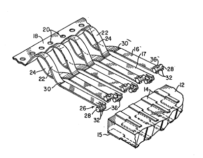
Fig. l is a perspective view of a solderable electrical
lead array for attachment to contact pads on a substrate, such
as a printed circuit board and the like, constructed and
arranged according to a preferred embodiment of the present
invention, in a condition ready to be assembled to the
substrate.
Fig. 2 is a perspective view of khe lead array of Fig.
1 showing it attached to contact pads on the substrate.
Fig. 3 is a partial end view of the solderable lead
array of Fig. 1 as seen from the distal or terminal end of the
leads.
Fig. 4 is a side view of the solderable lead array of
Fig. 1.
Fig. 5 is a side view of the solderable lead array of
Fig. 2 attached to the substrate.
Fig. ~ is a partial top plan view of a blank for use in
forming the solderable lead array of Fig. 1.
Fig. 7 is a fragmentary plan view of a modification of
the terminal end of the blank of Fig. 6.
Fig. 8 is a fragmentary elevation cross-sectional view
of the terminal end of Fig. 7, enclosing a solder mass and
assembled to a circuit board.
Fig. 9 is a fragmentary plan view of another modifica-
tion of the blank for the terminal end.
Fig. 10 is a fragmentary elevation cross-sectional view
of the blank of Fig. 9 formed to enclose a solder mass and
assembled to a circuit board.
Figs~ 12 show views similar to Figs. 9-10 for a
different distal end configuration for a ~olderable lead
according to the present invention.
Figs. 13-14 show similar views of a blank and another
distal end config~ration for a solderable lead according to the
present invention.
Figs. 15 and 16 show similar views for yet another
distal end configuration for a solderable lead according to the
present invention.
1~32a~
Figs. 17 and 18 show similar views for still another
distal end configuration for a solderable lead according to the
present invention.
Figs. 19 and 20 show similar views for a further distal
end configuration for a solderable lead according to the
present invention.
Figs. 21 to 23 show psrspective views and a side view,
similar to Figs~ 1-3, of an embodiment of a solderable lead
array constructed accordin~ to the present invention having
still another form of distal end.
Fig. 24 shows a perspective view of enlargements of the
distal end of a variation of the configuration, showing both
the upper and lower lead ends.
Fig. 25 shows similar views of another embodiment of
~5 the upper and lower distal end configuration.
Fig. Z6 shows a fragmentary side elevation cross-
sectional view of a further embodiment of a distal end
configuration, carrying a solder mass in a curved channel for
direct contact with the substrate to which the lead array is to
be solderad.
Fig. 27 shows a fragmentary side elevation cross-
sectional view of still yet another distal end configuration,
with the solder mass held in place by an extreme curved end
portion bent to conform with the solder mass shape and an
upwardly bent angular tab adapted to engage the opposing side
o* the solder mass.
! Figs. 28 and 29 show a fragmentary plan view and side
elevation cross~section of another distal end configuration
with sloping tabs bent relative to the plane of the lead such
that the solder mass i5 held in direct contact with the
substrate.
Fig. 30 is a top plan view of a blank of a comb-like
array of leads for another embodiment of the invention.
Figs. 31 and 32 show side elevation view of a modified
lead array according to the present invention using a blank
similar to that of Fig. 30 and with a distal end configuration
similar to that of Fig. 1.
~ 7 ~2 ~2 ~jg
Fig. 33 is a perspective view of another embodiment of
the present invention, with a distal end configuration that
carries a solder mass and a protruding perpendicular finger
adapted for engagement with through holes provided in the
substrate to which the lead array is to be attached.
Fig. 34 shows a partial top plan view of a lead array
useful in the embodiment of Fig. 33.
Figs. 35 through 38 show various embodiments of lead
constructions according to the present invention with different
distal end configurations that are designed to engage with
through holes formed in the substrate to which the lead array
is to be attached.
Fig. 39 shows a fragmentary plan view of a blank useful
in making the lead array of Figs. 40 and 41.
Figs. 40 and 41 show a modified version of the present
lead construction, similar to Figs. 1 and 2, with opposed leads
having a fulcrum for permitting opening of the distal ends of
the lead array to receive a substrate to which the leads are to
be soldered.
Fig. 42 is ~ fragmentary side elevation cross-section
of the ends of a lead array similar to Figs. 40-41, as
assembled in a circuit board, before soldering.
Description of the Preferred Embodiments
Referring now to the drawings, where like parts are
designated by the same reference numeral throughout the several
views, there is shown a preferred embodiment in Figs. 1-6
comprising an electrical contact lead structure 10 which is
adapted to be electrically connected to a substrate 12 carrying
electrical components and including electrically conductive
areas or contact pads 14. The structure is formed from a blank
as shown in Fig. 6, which essentially comprises a flat sheet of
conductive resilient material, such as beryllium copper, formed
into a substantially comb-like configuration with a row of
contact leads in the form of strips 16 flexibly carried from
one end by means of a common carrier strip 18. The strips 16
are separated by slits 17, preferably formed by cutting without
8 ~ 6g
removal of material, permitting utilization of the maximum
amount of material with less waste. The pitch of these strips
16 should be equal to one-half the pitch of the contact pads on
one side of the substrate intended to cooperate with these
leads which also has a plurality of sprocket holes 20 disposed
along the length thereof for use in moving or indexing the
structure 10. The leads 16 have an elongated configuration and
are made from a flexible and resilient metal such as beryllium
copper which has good electrical conductivity characteristics.
At the stem end of the leads alternate ones of the contact
leads 16 are bent upwardly as shown at 22 in an arcuate shape
or bow relative to the general plane of the lead structure,
while the intermediate leads are bent in their stem end
portions downwardly as shown at 24 to provide an opposite
arcuate bowed con~iguration relative to the plane of the lead
structure.
At the free or distal end of each lead 16 shown in
Figs. 1-6, there is provided a distal end configuration 26
designed for carrying a solder mass 28 which upon heating with
the lead in contact with a contact pad of th~ substrate as
shown in Fig. 2, and then cooling, will electrically connect
the lead with the substrate~ The distal end configuration 26 of
this embodiment shown in Figs. 1-6 comprises a pair of slits 31
defining a pair of spaced tabs 32 with an intervening finger.
The finger 36 is bent around a solder mass 28 to hold it
between the finger 36 and the opposing flat tabs 32. The
solder mass may have a width which substantially corresponds to
the width of each of the strips 16 as best shown in Fig. 3
although it may be longer, if desired. As best illustrated in
Fig. 6 the finger 36 extends lengthwise of the contact strip 16
beyond the termination of the flat tabs 32 to provide suffi-
cient length to partially encompass and hold $he solder mass
28.
The leads as shown are constructed and arranged to
cross one another such that when the portions 22 and 24 are
squeezed toward one another~ an opening is created between
th~ir ends 32 so that the edge of a substrate may be interposed
~ 9 ~ ~3X469
between those ends, as shown in Fig. 5.
The contact pads 14 on the upper face of substrate 12
ar~ spaced apart in correspondence to the spacings of the
copper set of leads 16l and the contact pads 15 on the lower
face of the substrate 12 are placed intermediate the upper pads
14, and in correspondence to the spacings of the lower set of
leads 17. Accordingly, when the tips 32 are separated by
pressure on the bowed portions 22, 24, the substrate 12 can be
interposed between these tips. When the pressure is relaxed
the resiliency o* the strips 16 causes the solder bearing ends
to contact respective contact pads 14, 15. This causes the
ends 32 to grip the substrate 12, and holds the contact comb in
place for subsequent heating to melt the solder, to make good
electrical contact on cooling. This arrangement facilitates
using a single mechanism for applying pressure to all of the
concave and convex portions 22, 24 simultaneously thereby
facilitating assembly of the lead structure to the substrate.
It will be understood that the ends of the contact
strips may have various con~igurations, either for holding
solder masses or for other direct contact with circuit board
contact pads.
Figs. 7 and 8 show another distal end configuration for
each of the lead strips 16. Here, the blank shown in Fig. 7
has the finger 42 shorter than the side tabs 40. As seen in
Fig. 8, both the finger 44 and the tabs 40 are bent around the
solder mass 28. The tabs 40 are bent in a curved fashion away
from the plane of the lead strip 16 to form a first side of a
channel 38 for the solder mass 28 and the finger 42 is also
bent in a curved fashion opposite to that of tabs 40 to define
the other side of the arcuate channel 38. The finger 42 and
tabs 40 may encircle the solder mass by more than 180 degrees
or one or the other may be crimped into the solder mass, to
hold it in place. Here again (as in all of the solder holding
arrangements) the solder mass preferably is as long as or
longer than the width of the contact strip 16 on which it
rests.
Figs. 9 and 10 show another embodiment of the distal
3Z~69
- 10
end configuration. Here the blank 26 (Fig. 9) has a slot 46
formed in it. As seen in Fig. lO, the end 48 is bent and/or
crimped around the solder mass 28 to hold it in place. The
slot 46 is between the solder mass 28 and the contact pad 14 to
allow the solder ~when molten) to flow (or be drawn by
capillary action) into the space between the contact lead 16
and the contact pad 14, to maXe a good electrical connection
when re-solidified.
Figs. ll and 12 show a further embodiment of a distal
end configuration, similar to the one shown in Figs. 9 and 10,
except that the slot 46 is extended to the end of the contact
strip 16, to form two elongated tabs 49 which are bent to
substantially encompass the major portion o~ the periphery of
the solder mass 28.
Figs. 13 and 14 show a lead having a distal end
configuration where a tab 52 is cut out and bent upwardly from
contact strip 16. The extreme end 50 of the lead strip 16 is
bent to form a cradle partially around the solder mass 28. Tab
52 is bent into the solder mass 28 on the side opposite from
the strip end 50 to hold the solder mass 28 in place on the
lead structure. The opening from which the tab 52 is cut
permits the molten solder to flow between contact strip 16 and
contact pad 14, as is desirable.
In the embodiment of Figs. 15 and 16, the Pnd 53 of
~5 each of the lead 16 is shown as having a distal or terminal
contact configuration similar to that of the embodiment of
Figs. 7 and 8. However, the free end portion 54 of each of the
leads is bent at a right angle relative to the lead strip 16
such that the lead extends perpendicularly to the substrate and
the solder mass can be disposed in direct contact with the
substrate contact pad to which the lead i5 to be secured. This
arrangement is particularly useful for leads for surface-
mounted components. In the embodiment of Figs. 17
and 18, the solder mass is held in place by a distal end
configuration similar to that as disclosed in the Seidler U.S.
Patent 4,605,278. In this arrangement, a pair of tabs 56
disposed on each side of the strip 16 are bent upwardly to
ll2~324~9
define a gap 58 which forms a channel extending transversely
across the width of the strip 16 between its lateral edges. The
solder mass 28 is disposed in this channel and is held by
bending the tabs 58 to hold the solder. A slotted opening 60
in strip 16 disposed in alignment with the main axis of the
lead may be provided such that when the solder mass is melted
it flows through the opPning 60 to making good electrical
contact between the lead and the contact pad underlying the
lead.
If desired, the end configurations shown in Fig. 18 may be
interchanged, with the one shown on top of the substrate being
placed at the bottom and vice-versa.
Another embodiment is shown in Figs. 19 and 20 in which
the end of the lead 16 is bifurcated, with two arms 62 which
retain the solder mass 28 crimped between them. In this
instance, the solder mass ~usually in the form of a short
section of solder wire) extends perpendicularly to the plan of
contact lead 16, and as shown in Fig. 20 is positioned directly
in contact with the contact pads 14 or 15.
Another embodiment is shown in Figs. 21 to 23, which
utilizes the blanks of Fig. 6. In this version, at the
terminal end of each lead, the configuration for holding the
solder mass in plane comprises a pair of spaced tabs 32
essentially in the place of the contact lead 16. A curved
finger 36 cut out from the end o~ contact lead 36 substantially
surrounds the solder mass and holds it in place at the terminal
end of the lead. In this instance, the finger 36 of each lead
end is juxtaposed to the contact pad 14 or 15, in contrast to
Fig. 2 where the tabs 32 are positioned against the contact
pads.
As in Figs. 1-2, the terminal end of each lead is
constructed and arranged so that when pressure is applied
between the bowed portions of the leads near the stem end, the
distal ends separate to accommodate the substrate to be
soldered, and upon release of the pressure the curved finger 36
will be disposed in contact with a respective contact pad as
best illustrated in Fig. 22.
.
`~ 12 ~ X~69
Fig. 24 shows another variation of terminal end for
contact strip 16, utilizing the blank of Fig. 7. Here, for the
upper contact lead, the solder mass is held against center tab
42 by a pair of spaced, bent, curved tabs 40 which define an
opening 68 disposed between them. On the opposing side for the
lower contact lead, the solder mass 28 is held similarly, but
in upside-down relation between flat central tab 42' and the
pair of curved fingers 40' In the arrangement of Fig. 24 when
the leads are disposed in contact with the substrate contact
pads, the curved fingers 66 will be disposed in contact with
the substrate.
Fig. 25 shows a variation similar to Fig. 24, but with the
upper and lower lead ends interchanged, so that the flat tab 42
is disposed in direct contact with the contact pad 14 or 15.
Fig. 26 illustrates a contact end configuration which
is like Fig. 8, but with each end turned over, so that the
channel 72 carrying the solder mass 28 is disposed in direct
contact with the suhstrate to which it is to be soldered. The
solder mass is held between curved outside tabs 74 and a
further curved center tab 76. The embodiment of Fig. 27 has a
configuration like Figs. 13 and 14, but with each end turned
over, so that the solder mass 28, when assembled with the
substrate is in direct contact with the respective contact pad
Similarly, the lead end of Figs. 28 and 29 corresponds
to that of Figs. 17 and 18, but turned over so that each solder
mass is assembled in direct contact with its contact pad, being
urged toward the contact pad by the resilience of bowed portion
22, 24.
In this embodiment no opening in the main lead directly
below the solder since the solder (such as 60 of Fig~ 17) need
be provided, since the solder mass is now disposed for direct
electrical contact with the contact pad, thereby improving the
manufacturing process.
Figs. 30-32 show an alternative way of providing the
comb arrangement of leads of the present invention, which
provides advantages in manufacture, at the cost of increased
waste of material. In the embodiment illustrated in Fig. 30-
13 ~ 69
32, the lead structure is made from a flat piece of sheet metalillustrated in Fig. 30, which comprises a left half 82 from
which a first set of the leads are formed (such as for above
the substrate) and a second contiguous right half 84 from which
the other alternate leads are formed (such as for below the
substrate). The two sets of lead blanks 82 and 84 are joined
by and integral with a central section 82, which may have one
or more sets of sprocket holes 83 for indexing the sheet during
manufacture. To form the comb-like lead structure of the
present invention, one of the halves 84 is folded along the
central fold line 86 such that the leads 16 in the half 82 will
be located between adjacent leads 16' formed in the other half
84.
The sprocket holes 83 may overly one anothsr, to form a
single set for use in automated assembly of the present
invention to circuit boards.
The structure shown in Figs. 31 and 32 has the solder-
bearing lead terminals o Figs. 1-5. It will be understood
that any desired terminal structure may be substituted,
including that of any of Figs. 7 to 29.
The embodiment of Figs. 33 through 35 provides a
construction and arrangement similar to the other embodiments,
adapted for improved mating of the lead structure with the
substrate. This version is designed for attachment with a
substrate 12 which, instead of or in addition to contact pads,
is provided with contact through-holes or openings 88 which are
disposed along the edge of the substrate) each adapted for
attachment with a corresponding lead. Each through-hole 88 may
be lined with conductive material and is optionally provided
with a flat contact pad 90 on the side of the substrate to
which the electrical connection is to be made. The terminal
end of each lead 16 has a configuration which includes a
protruding prong 96, formed as an extension of the end of lead
strip 16, the prong 96 being is disposed in substantially
perpendicular relation to the main plane or body of each of the
leads 16. The lead structure may be formed from a blank in the
form shown in Fig. 34, where the lead strips 16 are joined to
14 ~ 24~9
the carrier strip 18 as in Fig. 1. The end of each lead strip
16 is formed into a center Einger and side fingers 92. The
center finger becomes prong 96 when bent at a right angle to
lead strip 16. The direction of the prong 96 is such that when
the lead structure is assembled with the substrate, each of the
protruding prongs 96 is engaged in a corresponding one of the
through-holes 88, as best illustrated in Fig. 35. This aids in
properly aligning each lead end with its respective contact
pad. The resilient scissor-like action of the lead structure
causes the structure to be resiliently held on the substrate,
until a subsequent soldering actions, which may be by conven-
tional wave-soldering or dip-soldering.
Alternatively, in addition to prong 96, each lead end
is provided with a solder~retaining configuration, which holds
a solder mass adjacent the base of prong 96. As shown in Figs.
33 and 34, this may be formed by the outer pair of fingers 92,
which are bent around solder mass 28 to hold it in place
adjacent the base of prong 96. The space 94 between curved
fingers 92 permits ready solder flow to the contact pad. Thus,
when heat is applied to assembly of lead structure and
substrate, the molten solder will flow both between lead 16 and
the contact pad, and also into the substrate hole 88, to
provide electrical contact between the lead and the contact pad
surrounding the through-hole 88, as well as between prong 96
and the wall of the hole 88.
Figs. 36 and 37 show an alternative in which the solder
mass 28 is held between an elongated finger 102 (whose end
forms a prong to mate with the circuit board hole 88) and the
side tabs 104.
Fig. 38 illustrates another contact end configuration
where the hole-engaging prong 98 is formed at the extreme end
of the lead, and is bent at a right angle relative to the main
plane or body of the lead 16, so that the prong 98 engages the
substrate when the lead is assembled to the substrate. The
prong 98 provides a flat surface support on one side for the
solder mass 28 and on the other side the solder mass 28 is
supported by a sloping outwardly bent tab 100 which contacts
` 15 ~24~9
. . .~
the opposing surface of the solder mass 28 and maintains it in
position at the terminal end of the lead.
The embodiment in Fig. 39 illustrates the end of the
lead as being bent at right angles such that, when the leads
are assembled with the substrate, the end portions 106 will
align themselves with the corresponding through-holes and will
securely hold the lead structure to the substrate. The
embodiment of Fig. 39 is shown without any solder mass, since
it is not necessary within the scope of the invention to have
the solder mass carried by the lead structure; the lead
structure can be attached to the substrate by other suitable
means such as by applying the solder to the lead and substrate
after the lead has been attached in the manner shown in Fig.
39.
The further embodiment illustrated in Figs. 40-42 shows
a lead structure according to the present invention which is
also formed from a single continuous sheet or wide strip 108 of
metal having resilient characteristics and good electrical
conductivity. As Fig. 42 illustrates, tha leads are formed on
each of the two halves of the sheet 108 with the leads on one
side aligned with those on the other side of the sheet 108.
Each lead on one side of sheet 108 has a resilient howed
portion 22, and a reverse bend 112. The corresponding lead on
the other side of sheet 108 has a similar resilient bowed
portion 24 and a reverse bend 114~ The sheet 108 is folded on
itself, at or in the vicinity of line 110, so that the
corresponding bends 112, 114 are in contact, with the bowed
portions 22, 24 opposed to one another. The bends 112, 114
form a fulcrum or pivot, as shown in Figs. 40 and 41. This
fulcrum arranyement enables the lead ends to be separated to a
desired spacing by squeezing the bowed portions 22, 24
together, which pivots the leads 16 at the fulcrums 112, 114 to
separate the lead ends, permitting insertion of the substrate
to which the leads are to be attached. Since the lead pairs
are aligned in overlying relationship, the substrate to which
the leads are to be attached will have contact pads that are
similarly aligned above and below the substrate, instead of
.
16 ~.82~6~
being offset or interleaved as illustrated in the earlier
el~bodiments of the present invention. In this latter embodi-
ment, pressure may be exerted on the leads in the pressure
areas which is translated to the fulcrum point for each pair of
overlying leads to cause the opposed ends of the leads to open
to the desired spacing, correlated to the size of the sub-
strate. As in the case of the previously described embodiment
with scissor-like operation, the present lead structure permits
opening of all of the lead pairs simultaneously and placement
of the substrate for attachment with the leads in essentially a
single manipulation.
While the embodiment of Figs. 40-42 has been il-
lustrated as having solder-bearing lead ends with the con-
figuration of Figs. 1-5, it will be understood that any
solder=bearing lead ends, such as those described above, may be
used in this embodiment, or any other embodiment of the comb-
like structure.
While most of the embodiments have been described above
as having a solder mass at the terminal end of the lead that is
not essential. It is within the contemplation of the present
invention for solder to be applied separately as by a wave-
soldering or dip-soldering technique, after the lead has been
attached with the particular substrate to which it is to be
connected. Thus, ~y way of illustration, Fig. 42 shows the
lead end portions of the configurations of Figs. 40-41, with
the solder mass omitted. Here, the prongs 106 are bent
inwardly to engage the substrate hole 88 from both sides. The
resiliency of the bowed portions 22, 24 will retain the contact
configurations attached to the substrate through subsequent
soldering operations, which may be o~ conventional type.
Also, in any of the forms shown in Figs. 35 to 38, the
solder mass may be omitted. The prong 96, 98 or 102 will serve
to hold the comb-like lead structure on the substrate during
subsequent soldering.
After soldering is completed, the carrier strip and
bowed portions are removed, as by severing along line 23 or
Fig. 4 or Fig. 5 or a corresponding position in the other
-17-
embodiments. The lead strings may be scored as at 30 to facilitate
such severing. This leaves the leads 16 electrically and mechanic-
ally connected to the substrate at its contact pads, for use in
connecting to other circuit components. In some case, these leads
may serve as a multi-pin connection, directly mating with a
corresponding multiple receptacle.
In each instance, the lead terminal end is urged toward
its contact pad by the resilience of the spring bows 22, 24.
Thus, it will be seen that the present invention provides
a comb-like array of leads, each having a solder mass and/or a
locating structure at a terminal end, the array being in two sets
for respective attachment to conducting areas on the top and bottom
surfaces of a substrate, the leads being pivotable either at their
stem end (as in Figs. 1-2, 21-22 and 31-33) or at an intermediate
fulcrum (as in Figs. 40-41). Resilient structures in the form of
resilient bowed portions are formed in the leads, so that upon
applying appropriate force to the resilient structures, the sets
of leads are separated to accept a substrate (e.g~, a printed
circuit board) therebetween, with the lead terminal ends aligned
with respective contact pads on the substrate, and so that upon
releasing such force, the leads will tend to return to their
initial positions and thereby resiliently clamp the lead structure
to the substrate, to be held there during subsequent soldering.
The leads after assembly to the substrate may be severed
along a weakened area defined by the score line 30 to leave them at
a predetermined length for attachment to other components and items.
-17a- ~2~9
It should be understood that the present lnvention is
subject to many variations, modifications and changes in detail.
However, it is intended that all matter contained in the
foregoing description or shown in the accompanying drawings shall
be interpreted as illustrative only and not in a limiting sense,
the scope of the invention being defined by the appended claims.