Note: Descriptions are shown in the official language in which they were submitted.
~X~24~2
01 The present invention concerns a data
02 packet switching system and, more specifically, a
03 routing switch centre usable in a data packet
04 transmission network.
05 In a hierarchical transmission and
06 switching network, the routing switch centres process
07 considerable amounts of traffic. When, in a network,
08 the number of routing switch centres increases, the
09 mesh of interconnections becomes complicated. Large
routing switch centers have to be provided in order to
11 reduce the complexity of the mesh of
12 interconnections. This problem is not restricted to
13 data transmission networks; it already existed in
14 telephone switching networks, in which are provided
besides the regular routing centres, a few national
16 routing centres. Of course, the problem will exist on
17 integrated services digital networks ISDN currently
18 under development.
19 The French data packet transmission and
switching network TRA~SPAC~, which presently has 25
21 switching centres, already requires the use of routing
22 switch centres. The routing centres which have been
23 developed for this purpose have, however, a traffic
24 limit of 7500 packets per second. This limited
processing power would lead to an increase in the
26 number of the routing centres with an ensuing complex
27 synchronization.
2~ One aim o~ the present invention consists
29 in providing a large switching and routing centre
which can switch up to 100,000 packets per second.
31 The performances of known packet switching
32 systems are actually limited by the use of complicated
33 transmission procedures, the use of large buffer
34 memories, and the use of existing computing system
architectures. In this respect, in computing systems,
36 the exchanges of data are carried out by conventional
37 low speed buses which limit the traffic to the
38
39 ~ - Trade mark
,,~, ~
. . .i;
32~2
01 above-mentioned 7500 packets per second.
02 In accordance with a feature of the
03 invention, there is provided a data pacXet switching
04 system comprised of a plurality of input modules
05 receiving the ingoing packets, a plura1ity of output
06 modules transmitting outgoing packets, a double access
07 central memory divided into routing modules and a
08 resource control module, having also an input time
09 division bus to connect in time-division mode selected
input modules to selected routing modules respectively
11 in the central memory and an output time-division bus
12 to connect in time-division selected routing modules
13 in the central memory to selected output modul0s
14 respectively, the resource control module being
bidirectionally connected to the input modules and to
16 the centra1 memory by the input time-division bus, on
17 one hand, and to the output modules and the central
18 memory by the output time-division bus, on the other
19 hand.
In accordance with another characteristic,
21 each time-division bus, be it input or output, has a
22 plurality of sets of data wires each transmitting
23 parallel bytes of data, and a set of time-aivision
24 identification wires transmitting the id0ntifications
of time intervals forming recurrent frames of time
26 intervals, each frame containing 2k time intervals
27 and, in the sequence of frames, the time intervals
28 time spaced 2kl intervals apart, with kl less than k,
29 forming a time transmission channel, the time-division
channels being 2k-Xl in number, one of the said
31 time-division channels being reserved for signalling
32 messages between the modules, either of input, or of
33 output, and the resource control module.
34 In accordance with another feature, within
the time-division channel reserved for signalling
36 messages the time intervals are each allocated to a
37 module.
38 - 2 -
8;;~
01 In accordance with another characteristic,
02 within the time-division channel reserved for
03 signalling, the even (or odd) rank time intervals are
04 allocated to the input or output modules respectively,
05 depending whether it is an input or an output
06 time-division bus, and the odd (or even) rank
07 intervals to the resource control module.
08 In accordance with another feature, for
09 each packet transmission to the central memory carried
on the input time-division bus or from the central
11 memory carried on the output time-division bus, is
12 assigned a time-division channel selected among the
13 time-division channels other than the time-division
14 channel reserved for the signalling.
In accordance with another feature, the
16 plurality of sets of data wires consists of a first
17 set of wires used to transmit data packet or input or
18 output module identi-fications, a second set of wires
19 used to transmit routing module identifications, a
third set of wires used to transmit end of packet
21 signals, and a fourth set of wires being used to
22 transmit channel assignments.
23 In accordance with another feature, in the
24 input time-division bus, the first set of wires is
used, firstly, in the even (or odd) rank interval
26 assigned to an input module, to transmit from this
27 input module to the resource control module the
28 routing data of a packet to be switched, then, in
29 response thereto, in one of the odd (or even) rank
intervals of the timing channel reserved for the
31 signalling messages, the identity of the same input
32 module which receives in the same time interval,
33 through the fourth set of wires, the identification of
34 the assigned channel, the memory also receiving, in
the same time interval, the identity of the assigned
36 channel by the fourth set of wires plus the identity
37 of the selected routing module to store the packet
38 - 3 -
~LZ~ 8Z
01 through the second set o~ wires, the exchange of
02 useful data being carried out on the first set of
03 wires in the successive time intervals of the channel
04 assigned between the input module and the routing
05 module selected for it, up to the last byte of the
06 packet which is accompanied by the end of packet
07 signal transmitted on the third set of wixes and
08 received simultaneously in the memory and the resource
09 management module.
In accordance with another feature, in the
11 output timing bus, the first set of wires is used,
12 firstly, in the odd rank (or even) interval of the
13 time-division channel reserved for signalling
14 messages, to transmit the identity of the output
module intended to transmit the packet, said output
16 module receiving in the same time intexval the
17 identity of the assigned channel, the memory also
18 receiving, also in the same time interval, the
19 identity oE the channel assigned through the fourth
set of wires plus the identity of the routing module
21 in which is stored the said packet through the second
22 set of wires, the exchange of useful data from the
23 stored packet being carried on the first set of wires
24 in the successive time intervals of the channel
allocated between the routing module up to the last
26 byte -from the packet which is accompanied by the end
27 of packet signal transmitted on the third set of wires
28 and received simultaneously in the output module and
2~ the resource management module.
The features of the above-mentioned
31 invention, as well as others, will become clearer upon
32 reading the description of an embodiment, the said
33 description being carried out in relation to the
34 attached drawings, among which:
Figure 1 is a general block diagram of a
36 routing switching centre in accordance with the
37 invention,
38 - 4 -
32
01 Figure 2 is a timing diagram illustrating
02 the operation of the input or output time-division bus
03 of the switching centre of Figure 1,
0~ Figure 3 is a schematic block diagram of
05 an input module of the switching cen~re of ~igure 1,
06 Figure 4 is a diagram illustrating the
07 operation of the timer of the input module of Figure
08 3,
09 Figure 5 is a schematic block diagram of
the input interface of the control module of the
11 switching centre of Figure 1,
12 Figure 6 is a schematic diagram
13 illustrating the op0ration of the control module in
14 the input resource search mode,
Figure 7 is a schematic block diagram of a
16 portion of the control processor inside the control
17 module,
18 Figure 8 is a schematic block diagram of
19 the output interface of the control module,
Figure 9 is a diagram illustrating the
21 operation of the control module in the output resource
22 scanning mode, and
23 Figure 10 is a schematic block diagram of
24 an output module in the switching centre of Figure 1.
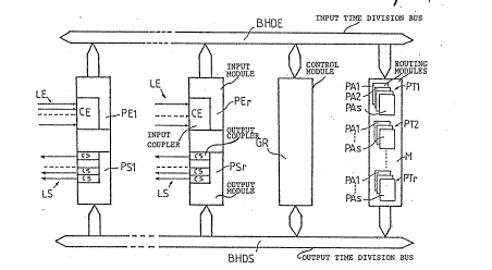
The route switching centre of Figure 1
26 consists of a plurality of input modules PEl to PEn, a
27 plurality of output modules PSl to PSn, a double
28 access central memory M, a resource control circuit
29 GR, an input time-division bus BHDE, an output
time-division bus BHDS. The switching centre may also
31 have a data processor bus.
32 Each of the input modules PEl to PEn is,
33 on one hand, connected through an input coupler CE, to
34 a number of input lines LE which transmit data packets
to it and, on the other hand, to the input
36 time-division bus BHDE to which it transmi-ts on a
37 time~division mode the contents of the packets
38 - 5 -
01 received from the associated input coupler CE.
02 ~ach of the output modules PSl to PSn is
03 connected, on one hand, through output couplers CS, to
04 a number oL output lines LS to which it transmits data
05 packets to be transmitted and, on the other hand, to
06 the output time-division bus BHDS which sends it the
07 data packets in a mode.
08 The central memory M is a double access
09 memory, one access being connected to the input
time-division bus BHDE for writing and the other
11 access being connected to the output time-division bus
12 B~IDS for reading. The memory M is, in practice,
13 divided in segments PTl to PTr, themselves divided
14 into pages PAl to PAs. One page PAj in a segment PTi
makes up a routing module PTi, PAj.
16 The resource management module GR has a
17 control processor containing a microprocessor, and two
18 interfaces, one for the access to the input
19 time-division bus BHDE and the other for the access to
the output time-division bus BHDS. The microprocessor
21 of the control module GR can be selected from the
22 microprocessors specifically designed for switching
23 centres, in particular data switching centres.
24 ~he buses BHDE and BH~S are high speed
time-division buses on which the data are transmitted
26 on time-division channels which are defined on
27 recurring time frames. Each frame has 2k time
28 intervals. As in the example described, k=8, each
29 frame has 256 time intervals IT0 to IT255. In Figure
2, there is shown a frame Ti, preceded by the frame
31 T(i-l) and followed by the frame T(i~l). In each
32 column of the frame Ti of Figure 2, the time intervals
33 follow one another and when the bottom of a column is
34 reached, the subsequent time interval is at the top of
the next column. In the other direction, the time
36 intervals are grouped into eight rows C0 to C7. In
37 the switching system of the invention, each row of the
3~ - 6 -
~3Z~32
01 unbroken sequence of frames corresponds to a channel
02 Ci.
03 In the two time-division buses BHDE and
04 BHDS, the first channel or channel C0 is reserved for
05 signalling. Thus, the channel C0 of bus BHDE serves
06 for the signalling exchanged between, on one hand, the
07 control module GR and, on the other hand, the input
08 modules PEi and the input access of memory M. The
09 channel C0 of bus BHDS is used for the signalling
exchanged between, on one hand, the control module GR
11 and, on the other hand, the output modules PSi and the
12 output access of memory M.
13 Each of the other channels Cl to C7 of bus
14 BHDE can be assigned to an input module the time
necessary for to transmit a data packet to the input
16 access of memory M. Each of the channels Cl to C7 of
17 bus BHDS can be assigned to an output module PSi the
18 time necessary for an output access from memory M to
19 transmit it a data packet. The assignment of one of
the channels Cl to C7 is controlled by signalling ~rom
21 the control module GR.
22 The buses BHDE and BHDS are identical and,
23 as detailed in Figures 3 and 10 each consist of nine
24 wires D0 to D8 used to transmit data bytes in parallel
and a STOP signal, three wires D10 to D12 used to
26 transmit the channel number K, eight wires D20 to D27
27 used to transmit the identity of the time intervals
28 IT0 to IT255, eight wires D30 to D37 used to address a
29 routing module PTi, PAj in the central memory M, a
wire D40 used to transmit a validation signal VALE and
31 a wire D50 used to transmit a clock signal H.
32 With regards to the operation of bus BHDE,
33 in channel C0, reserved for signalling, the sixteen
34 odd time intervals, that is IT8, IT24, , are
reserved for transmission from the control module GR
36 to the input modules PEl to PEn, with n less than or
37 equal to 16, and the sixteen even time intervals, that
38 - 7 -
2~
01 is IT0, IT16, , are reserved for transmission from
02 the input modules to the control module GR
03 respectively. In the ~ollowing, we shall designate
04 the time intervals of channel C0 by ITs~i) for the
05 even ranks, where i represents the iaentification of
06 an input module PEi, the set o-f time intervals ITs(i)
07 being designated by ITs, and ITge for the odd ranks.
08 In other words, a time interval ITs(i) identifies the
09 input module which transmits a signalling message to
the control module. On the entrasy, each time
11 interval ITge designates a message transmitted by the
12 control module, the identity of the input module being
13 contained in the message. With regards to the
14 operation of bus BHDS, we would find, in its channel
C0, the assignment of similar even and odd time
16 intervals, the output modules replacing the input
17 modules.
18 If we consider the words transmitted by
19 the wires D20 to D27, it is apparent that the three
most significant bits transmitted by D20 to D22
21 designate the active channel, when it concerns C0, the
22 bit transmitted by D23 defines the transmission
23 direction, and the four least signi~icant bits
24 designate the input ~or output) module involved in the
signalling.
26 Without going into details, but to better
27 comprehend the operation of the invention, we will
28 summarize below one phase of the operation of bus
29 BHDE.
When an input module PEi is ready to
31 transmit a packet, it transmits, through by wires D0
32 to D7, the routing byte of the packet concerned, that
33 is the first byte of that packet, in the even time
34 interval ITs(i) associated to it in channel C0. The
control module GR receives this routing byte and
36 proceeas to seek on idle routing module as on idle
37 channel from the channels C1 to C7.
38 - 8 -
~ ;~132~32
01 Once found the idle routing module PTi,
02 PAj and idle channel Ci, the control module GR
03 transmits, in the first subsequent free time interval
04 ITge, the number K of the idle channel to said module,
05 which recognizes its identity transmit-ted the bus data
06 wires D0 to D7. At each time interval of this channel
07 Ci, the input module will apply a data byte to the
08 wires D0 to D7. In the time inter~al where the last
09 byte of a packet is transmitted on channel Ci, the
input module concerned also transmits a "1" bit on
11 wire D8, that is the STOP signal, which is received in
12 the control module GR which may thus consider the
13 channel Ci as being idle again and assign it again to
14 one of the input modules, may be the same, for the
transmission of another packet.
16 Furthermore, during the same time interval
17 ITge where the number K of the channel allocated to an
18 input module PEi is transmitted, the control module
19 GR, transmits on wires D30 to D37 o the bus, to the
memory M the identity PTi, PAj of the selected routing
21 module. The number K of the channel will then serve
22 to the address memory module M, to direct the data
23 from the packet to the routing module. For example,
24 the bits transmitted on the wires D30 to D32 serve to
identity a segment PTl to PTr, and the bits
26 transmitted on the wires D33 to D37 serve to identify
27 a page PAl to PAs inside the segment. For example, a
28 page is provided to store a maximum of 256 bytes.
29 To simplify the following description all
the time intervals that are part of the same channel
31 number K, except the signalling channel, will have the
32 reference ITK. The signal VALE transmitted by wire
33 D40 accompanies each information transmission on the
34 bus, in one direction or the other. Finally, the
clock signal ~ whose rate is that of the time
36 intervals is assumed to be applied in each mode to the
37 circuits which need it.
38 _ 9 _
2~3Z
01 As an indication, the clock signal H has a
02 frequency of 8 MHZ, which, with the eight data wires
03 D0 to D7, corresponds to a maximum theoretical rate of
04 56 M bit/s.
05 With regards to the bus BHDS, the
06 structure and operation are analogous and are shown in
07 particular during the description of an output module
08 PSi, Figure 10.
09 Before describing in detail the different
modules of the routing centre, we recall that a FlF0
11 memory, called a file in the following, is provided
12 with a data input ED, a data output SD, a write enable
13 input SI, a read enable input S07 an output IR
14 indicating that the file is not full and an output OR
indicating that the file is not empty. We shall
16 consider in the following that the operation of a Eile
17 is well known.
18 Also, at the output of certain files are
lg placed buffers which have the role of transmission
gates transmitting with a small time delay, at their
21 outputs the informations applied to their inputs.
22 These buffers are used to avoid any interference
23 between circuits downstream of the files and their
24 outputs ED. These buffers transmit when they receive
an enable signal. Downstream of the buses, such
26 buffers are also used to do a good separation of each
27 bus from the utilization circuits.
28 An input module PEi, shown in Figure 3 is
29 associated with ingoing line couplers CE whose inputs
are connected to a number of ingoing lines LE. The
31 coupler CE is assumed to receive from the lines LE
32 data which are already arranged into packets each
33 containing their routing header. The coupler has a
34 buffer memory, not shown, into which it is supposed to
know how to arrange the packets going into a packet
36 file. In the example described, we assume that the
37 packets are made up of bytes of eight bits and that
38 - 10 ~
`8~2
01 the routing header is made up of a single byte. Of
02 course, in the ollowing one could consider bytes of
03 more than eight bits each. The structure of such a
04 coupler CE is known to someone practicing in the field
05 and in regards to ~his topic, reference may be made to
06 related literature on the French data transmission
07 system "TRANSPAC".
08 The coupler CE has a data output connected
09 to the first eight wires of the ED input of a data
file DON, an output wire STOPE connected, on one hand,
11 to the ninth wire of the ED input of file DO~ and, on
12 the other hand, to an input of an A~D gate Gl whose
13 output is connected by a wire SlF to the SI input of a
14 request file FOR, and a write enable wire which is
connected, on one hand, to a write input of data file
16 DON and, on the other hand, to the second input of
17 gate Gl. The files DO~ and FOR, as well as the gate
18 Gl are in the input module.
19 Each data packet delivered from the
coupler CE has a first routing byte. The end of a
21 packet is indicated by a "1" bit on the STOPE wire.
22 In the input module, the eight wires of
23 the SD output of data file DON are connected, on one
24 hand, to the input of a request register R~R, and, on
the other hand, to the input of a buffer BUFl. The
26 ninth wire STOP of the SD output of file DO~ is
27 connected, on one hand, to a corresponding input of
28 buffer BUFl and, on the other hand, to a control input
29 of timer SEQ. The file DO~ has its read input SO
connected to timer SEQ through a wire SODON and its OR
31 output connected to wire D40 of the bus through
32 register RER and buffer BUFl.
33 The request file FOR has its OR output
34 connected through a wire ORF to a control input of
timer SEQ and its read input SO connected through a
36 wire SOF to an output of timer SEQ. One control input
37 of regiser RER is connected, through a wire CRER, to
38
- ~2~ 32
01 an output of timer SEQ. The register RER also has a
02 validation input to which is applied the signal
03 ITs(i). The buffer BUFl has the signal IT~ applied to
04 its validation input. The timer SEQ also has two
05 control inputs to which are applied the signals ITs(i)
06 and ITs(i-l) respectively.
07 The output of register RER is made up of
~8 eight wires which are connected to wires D0 to D7
09 respectively of bus BHDE. Similarly, the output of
buffer BUFl is made up of eight data wires connected
11 to wires D0 to D7, plus a wire STOP connected to wire
12 D8.
13 The input module PE also has an
14 identification recognizing comparator RECE whose first
inputs are connected to wires D0 to D7 of bus BHDE, a
16 channel identity registrations register REK whose data
17 input is made up of three wires connected to wires D10
18 to D12, a buffer BUF2 whose data input is made up of
19 eight wires which are connected to wires D20 to D27
and a three input AND gate G2 whose first input is
21 connected to wire D40. The output of gate G2 iS
22 connected to a validation input of register REK and to
23 the clock input of a flip-flop FFl whose Q output is
24 connected to the validation input of a comparator
COMPK. The output of bufEer BUF2 and that of register
26 REK are connected to the two inputs of comparator
27 COMPK respectively whose output ITK iS connected to
28 the validation input of buffer BUFl. In other
29 respects~ the output of buffer BUF2 is connected to
the input of a decoder DECODE of which one output ITge
31 is connected to the second input of gate G2 and of
32 which another output is connected to an input of a
33 second comparator COMPE. The second input of
34 comparator COMPE is connected to the output of an
identity memory CARE which generates a signal
36 representing the identity of the input module PEi.
37 The comparator COMPE has two outputs ITs(i) and
38 - 12 -
.
~ ~Z~2
01 ITs(i-l) which are connected to corresponding inputs
02 o~ timer SEQ. The output ITs(i) is also connectea to
03 the validation input of register RER. The second
04 input of comparator RECE is also connected to the
05 output of the identity memory CARE and its output is
06 connected to the third input of gate G2.
07 The timer is preferably a PROM memory
08 serving to generate the control signals CRER, SODON
09 and SOF. As shown in the diagram of Figure 4, the
state of the timer SEQ goes through five phases at
11 each packet transmission:
12 ~ Phase O which corresponds to the wait
13 for an end of packet transmitted from
14 coupler CE to module PEi,
- Phase 1 which corresponds to the wait for
16 the time interval ITs(i-l) which precedes
17 the signalling ti~e interval assigned to
18 module PEi to address a request to the
19 management module,
- Phase 2 which corresponds to the wait for
21 the end of the packet transmitted to bus
22 HDBE,
23 - Phase 3 which coresponds to the wait for
24 the end of the transmission of the packet
to bus ~DBE,
26 ~ Phase 4 which corresponds to the detection
27 of emptying of file FOR.
28 The events that cause the timer to pass
29 from a phase HCO the following one are, in order, the
~ollowing:
31 - El which corresponds to testing the OR
32 output of file FOR, the OR output at "1"
33 indicating that a complete packet has
34 arrived into the input module PEi, being
understood that the input module cannot
36 send a request to the control module until
37 it has received a complete packet,
38 - 13 -
~`29L~
01 - E2 which corresponds to the detection of
02 ITs(i-l~,
03 - E3 which corresponds to the output of the
04 "1" bit on the ninth wire of the SD output
05 of file DON,
06 - E4 which correspon~s to the end of the
07 exchange between the input module and the
08 routing module.
09 The actions generated during each phase
are the following:
ll - T2 which corresponds to the loading of the
12 request register RER under the control of
13 the signal transmitted on wire CRER, that
14 is, to the loading of the routing byte in
RER, then the transmission of the signal
16 SODON,
17 - T3 which corresponds to the read command
18 SOF from file FOR,
l9 - T4 which corresponds to the end of reading
from the file FOR.
21 In the control module GR, the access
22 interface to bus BHDE, Figure 51 has three input files
23 GFOR, FNPE and FLRE and an output file FARE. In other
24 respects, it has a status register REGETAT. This
interface is connected to a microprocessor MP which is
26 part of the process controller. Thus, the files and
27 status registers are connected to the microprocessor
28 by a conventional interval bus BUSINT.
29 The OR outputs of the input files GFOR,
ENPE, FLRE are connected to wires ORFOR, ORFIT, ORFLRE
31 respectively, which are connected to corresponding
32 inputs of state register REGETAT. It has an output
33 connected by an input wire SIFARE, to the SI input of
34 file FARE, whose SO input receives the signal ITge.
The ED input of file GFOR is connected to
36 wires D0 to D7 of bus BHDE, that of file FNPE to wires
37 D24 to D27, and that of file FLRE to wires D10 to
38 - 14 -
" ,~,
~2~32~L82
01 D12. The SD output of file FARE is connected to wires
02 D0 to D7, D10 to D12 and D30 to D37 of bus BHDE.
03 The SI inputs of files GFOR and FNPE are
04 connected to the outputs of two AND gates G3 and G4
05 respectively whose first inputs are connected to wire
06 D40 to receive the signal VALE and whose second inputs
07 receive the inputs ITs. The SI input of file FLRE is
08 connected to the output of an AND gate G5 are input of
0g which is connected to wire D8 to receive a STOP signal
and the other to wire D40 to receive the signal VAL.
11 The SO inputs of files GFOR, FNPE and FLRE are
12 connected to bus BUSINT.
13 In practice, file NFPE is used to register
14 the identity of the input module PEi which, in the
time interval ITs(i) which identifies it in the
16 signalling channel C0, transmits a routing byte which
17 is received in ~ile GFOR. The enabled wires ORFO and
18 ORFIT transmit to register REGETATl a signal which is
19 stored in it and which indicates that a request is to
be processed by microprocessor MP. When the latter
21 looks up register REGETATl it seeks, on one hand, a
22 idle routing segment PTi and, in a segment, an idle
23 page PAj, and, on the other handt a idle channel Ci.
24 We shall see in the following how this search is
carried out. When the result of the search is
26 positive, the microprocessor MP signals to the status
27 register REGETATl that it activates the write eneble
28 control wire SIFARE of file FARE and, through bus
29 BUSINT, it transmits to file FARE the identity of the
channel. Ci to be used and the address of the routing
31 module PTi, PAj which will receive the packet
32 transmitted by the input module PEi on channel Ci.
33 The file FLRE serves to register the
34 identity of a freed channel at the end of a packet,
which is signalled by setting wire DI to "1" sending a
36 STOP signal.
37 The input interface, Figure 5, also has a
38 - 15 -
~Z~2~2
01 clock CLl, which distributes clock signals H on wire
02 D50, and a time base BT, connected to the clock CLl,
03 to supply the signals ITge and ITs corresponding to
04 the time intervals reserved for signalling to the
05 input modules or coming from these through channel C0
06 respectively.
07 The input interface, Figure 5, also has,
08 connected to bus BUSINT, a file FKE in which are
09 stored the number of the idle channels, and a table
TBE which stores the states of the routing modules
11 PTi, PAj of the memory module M.
12 The microprocessor MP, located in the
13 control processor, but connected to bus BUSINT, can
14 read the word stored in register ~EGETATl any time it
needs it. As a function of the number of "1" bits in
16 this word, it can achieve, through bus BUSINT, the
17 reading inputs SO of files GFOR, FNPE and FL~E. IT
18 also has access by reading and writing, to the file
19 FKE, to seek a idle channel, and to table TBE, to seek
for instance a idle segment PTi and, in that segment,
21 a free page PAj.
22 Without going into the details of the
23 memory M, we assume that it hasj ~or example, by seven
24 cards or segments PTi, whose coding requires 3 bits
and that each card or segment contains 32 pages PAj,
26 coded with 5 bits. Each page has, for example, a
27 maximum capacity of 256 bytes.
28 The memory M, of Figure 1, is assumed to
29 contain its own control circuits which, when they have
simultaneously received from ~he bus BHDE the identity
31 k of a channel and the identity of a routing module
32 PTi, PAj, can write the contents of the arriving
33 packet on this channel into the assigned page of the
34 assigned segment. Each page is associated to an
address pointer which is incremented for each byte
36 received in the page and whose incrementing is topped
37 by the stop bit accompanying the last byte of the
38 - 16 -
01 packet. The value of the pointers which measures the
02 length of the packet, is thus stored in an appropriate
03 area called the length memory.
04 Each page is also associated to an output
05 pointer whose content will, during the process of
06 reading a stored packet to the bus BHDs, be
07 continuously compared with the value stored in the
08 length memory such that a stop signal is generated
09 with the last byte of the packet.
We will now describe the operation of an
11 input module PEi and of the control module GR with
12 regards to the transmission of a packet entering by
13 the input module PEi towards a routing module PTi,
14 PAj.
By assuming that the file DON is not ~ull,
16 the input coupler CE, Figure 3, controls the SI input
17 of that file to write into it packet by input ED. The
18 words of the packets are bytes and a ninth wire is
l9 foreseen to transmit a bit at the end of each packet.
Each end o~ packet energizes through gate
21 Gl the write input of request file FOR and a "l" bit
22 is written in it. The OR output is energized and this
23 triggers the operating cycle of timer SEQ.
24 In other respects, on a continuous manner,
the buffer BUF2 follows the progress o~ the time
26 interval word transmitted by the wires D20 to D27.
27 This word is transmitted to decoder DECODE which
28 deducts the identities of successive time intervals of
29 channel CO, C', that is, on one output, the
transmitted signal carrying the same reference, and,
31 on the other output, the successive signals
32 corresponding to different input modules, either the
33 signals ITs(l), , ITs~i-l), ITSti)~ , ITs(16).
34 These signals are compared with the contents of the
3~ memory CAR in comparator COMPE, which for the input
36 module of rank i, generates a first signal at time
37 ITs(i-13, then a second signal at time ITs(i). The
38 - 17 -
1~82~L~X
01 first signal applied to timer SEQ, which is assumed to
02 have been activated by the OR output of file FOR,
03 causes the generation of the signal CRER which causes
04 the reading of the routing byte from the file DON to
05 the register RER. The next signal ITs(i) triggers the
06 reading of the CQntents of the register RER on the
07 wires D0 to D7.
08 At the instant ITs(i), the wires D20 to
09 D27 of bus BHDE also identify the same instant. Thus,
the files GFOR and FNPE of control module GR, Figure
11 5, register the routing byte and ITs(i) respectively.
12 If the file G~OR was previously empty, the OR output
13 puts, into the state register REGETATl, the bit
14 corresponding to a "1". The microprocessor MP, after
looking up the word in the state register REGETATl,
16 takes into consideration the input exchange request
17 and seeks an idle channel by referring to the file FKE
1~ and an idle routing module by referring to table TBÆ.
19 As long as the serach is negative, the microprocessor
MP does not modify the state of the files GFOR and
21 FNPE. As soon as the search is positive, the
22 microprocessor loads into file FARE, the identity K of
23 the channel read from file FKE and the identity PTi,
24 P~j of the idle routing module read from table ~BE.
It then translates the contents of the first word of
26 file F~PE to deduce the identity of the calling input
27 module and transmits this identity to file FARE.
28 If we assu~e that the file FARE was empty
29 before receiving these informations, at the next
instant ITge, the SO output of file FARE is enabled
31 and are transmitted on wires D0 to D7 of bus BHDE the
32 identity of the input calling module, on wires D10 to
33 D12, the identity k of the channel and, on the wires
34 D30 to D37, the identity of the routing module.
Through buffer BUF2, in the input module
36 PEi, Figure 3, the decoder recognizes a time interval
37 ITge and enables its corresponding output. In other
38 - 18 -
- ~ \
'~8;~ 12
01 respects, in comparator RECE, the identity of the
02 module is recognized. Thus, two inputs of gate G2 are
03 enabled, ~hen the signal VAL appears on the third.
04 The output of gate G2 enables register REK which
05 stores the identity k of the channel and sets the
06 flip-flop FFl such that ~he comparator COMPK operates.
07 As a result, each time that the identity
08 of the time interval on the wires D20 to D27
09 correspond to a time interval of channel k, the
comparator COMPK will enable the wire ITK and the
11 buffer BUFl will apply to wires DO to D7 a byte read
12 Erom file DON.
13 In parallel, in the module memory, the
14 above-mentioned control circuits has been set such
that at each time interval of the channel K, the byte
16 present on wires DO to D7 are stored into page PAj of
17 segment PSi. The address pointer assigned to that
18 page is incremented at each byte which is recei~ed.
19 When the last byte of the packet
transmitted by coupler CE appears at the output of
21 file DO~, it i~ accompanied of the stop bit "1". The
22 timer SEQ thus changes state and a "1" bit on wire D8
23 appears at the output of buffer BUFl. In the control
24 module GR, the gate G3 is thus enabled by its two
inputs, and the identity of the time interval is
26 stored in the file FLRE. Finally the flip-flop FFl,
27 is reset to zero, which inhibits comparator COMPK and
28 suppressed the signal ITK on buffer BUFl.
29 Gonsequently, the reading of file DO~ is interrupted
and the input module PEi stops transmitting.
31 In the control mode GR, the file FLRE is
32 read by microprocessor MP and the identity K of the
33 channel which has just been read is written into file
34 FKE.
The diagram of Figure 6 summarizes the
36 process followed by the microprocessor MP for the
37 assignment of input resources, that is the assignment
38 - 19 -
~2~32~82
01 of an idle channel and of an idle routing module. It
02 appears that, through bus BHDE, an input module PEi
03 places a routing byte into file GFOR. The
04 microprocessor MP then refers to the idle cha~nel file
05 FKE and table TBE which can consist of two files PTl
06 and PGL, one for the idle seg~ents, the other for the
07 idle pages. When the three OR outputs of files FKE,
08 PTL, and PGL are enabled the gate POR is opened to
09 allow the ~low of words read from those three files to
the input of file FARE. Si~ultaneously, the first
11 routing byte read in file ~FOR is transmitted for
12 processing ~icroprocessor MP which selects one file
13 from a number of files CMTl to CMT16 and writes into
14 it the identity of the routing module generated by the
files PTL and PGL.
16 In the portion of the control processor
17 shown in Figure 7, we find the microprocessor MP
1~ connected to bus BUSINT. A routing table ROOT,
19 connected directly to ~icroprocessor MP, allows when a
routing byte read from ~ile GFOR, Figure 5 is applied
21 to it, the translation of this byte into a link
22 address, that is, an output line LS address connected
23 to an output module PS.
24 In Figure 7, the data inputs of as many
files as there are output channels are connected to
26 bus BUSINT, that is in the example described with the
27 ED inputs of sixteen files CMTl to CMT16. Each file
28 CMTi has its ED input connected to bus BUSINT and its
29 output associated to a buffer REGi whose output is
connected by a local bus BUSLOC to the ED input of an
31 EXEC file. The SD output of the EXEC file is
32 associated to two buffers REG17 and REG18, the output
33 of buffer REG18 being also cGnnected to the ED input
34 of the EXEC file by bus BUSLOC while the output of
buffer REG17 is connected to bus BUSINT.
36 In Figure 7, are also shown for each file
37 CMTi, the write enable inputs SIi and reaa enable
38 - 20
~2Y3~ 32
01 inputs S0i, and the not empty state output O~i, as
02 well as for each associated buffer REGi, the
03 validation input VALi. The EXEC file also has the
04 inputs SIe and S0e as well as the output ORe.
05 Finally, the buffers REG17 and REGl8 have their
06 validation inputs VA17 and VA18.
07 As mentioned above, through bus BUSINT,
08 the microprocessor MP gets from the file GFOR the
09 routing byte and, after referring to the table ROUTI
deduces the identity of the outgoing channel on which
11 the packet will be delivered by the routing centre.
12 The microprocessor MP thus writes into the file CMTi
13 corresponding to the outgoing channel the address of
14 the routing module PTI, PAj provided to store the
packet.
16 Ea~h wire CMTi transmits, in addition to
17 its own identity, its coordinates to the EXEC file
18 which assembles the outgoing requests. We note that
19 there are 8 input wires to the CMTi files,
corresponding to the address of a routing module,
21 while there are 12 for the EXEC file to add the
22 identity of the CMTi file.
23 In practice, the reading of the contents
24 of the CMTi file into the EXEC file is controlled by a
read control circuit which is also shown in Figure 7.
26 We must observe that this control circuit operates in
27 such a manner that r in the EXEC file, there is a
28 single word at a time coming from a CMTi file. In
29 other wordsl there are not simutaneously two words
coming from the same CMTI file in the EXEC file.
31 For each word read into the EXEC file and
32 transmitted to microprocessor MP, through buffer REG
33 17, by bus BUSI~T, the microprocessor seeks, following
34 a procedure described in the following, if the
corresponding stored packet can be trans~itted. If
36 the result of the search is positive, it generates the
37 output cooperates. If the search is negative, the
38 - 21 -
, ~
~2~
01 word is rewritten in -the EXEC file through buffer REG
02 18.
03 The read control circuit of the CMTi files
04 and of the EXEC file has a state register which stores
05 an eight bit word, whose data input and whose loading
06 input are connected to ~he BUSINT bus, and whose
07 individual outputs are connected to the corresponding
08 inputs of an automation PALl. The four least
09 significant bits in the word stored in register
REGLEC, identify the CMTi files, the fifth indicates
11 the command to read the EXEC file to the
12 microprocessor, the sixth indicates the command to
13 simultaneously read, the EXEC file and the CMTI file
14 identified by the four least significant bits, the
seventh bit indicates the command to read the singly
16 designated CMTi file, and the eight indicates the
17 command to activate the buffer 18 to loop the word
18 read into the EXEC file to its input.
19 The circuit PALl also has a clock input H
and a control input ESOE, as well as a zero reset
21 output connected to an input of an OR gate G6 whose
22 output is connected to the zero reset input of
23 register REGLEC. The automation PALl translates the
24 informations applied to its data inputs to deliver its
individual read commands to the outputs SOl to SO16
26 and SOe of the EXEC and CMTi files.
27 The read control circuit also has sixteen
28 flip-flops FF2.1 to FF2.16 whose clocking inputs are
29 connected to the outputs ORl to OR16 of the CMTi to
CMT16 files respectively. The Q outputs of these
31 flip~flops, as in the eight bit output of register
32 REGLEC, are connected to the data inputs of an
33 automation PAL2 whose outputs are connected to the
34 validation inputs VAl to VA16 and VA18 to buffer REGl
to REG16 and REG18. The automation PAL2 also has a
36 clocking input H. Its purpose is to avoid access
37 conflicts among the files CMTi to the EXEC file.
38 - 22 -
01 The outputs VAl to VA16 of the automation
02 PAL2 are also connected to the zero reset inputs of
03 the flip-flops FF2.1 to FF2.I6 and to the inputs of
04 NAND gate G7 whose output is connected to the input of
05 an A~D ga-te G8.
06 The output VA18 is connected to the input
07 of an inverter INVl whose output is connected, on one
08 hand, to the D input of a flip-flop whose clocking
09 input receives the clock signa] H and whose Q output
is connected to the ESOE input of the automation PALl,
11 and on the other hand, to the input of an OR gate G9.
12 The second input of the OR gate is connected to the
13 output of AND gate G8 and its output is connected to
14 the SIe.
With regards to the operation of the
16 control processor of Figure 7, the microprocessor MP
17 is programmed to be master of each word to be stored
18 in the register REG~EC.
19 To read the EXEC file, it sets the 5th bit
of the word to "1", validates the buffer REG17 and
21 receives the identification of the output channel,
22 that is the identification of file CMTi, and the
23 identity of the routing module concerned. It searches
24 if the following conditions occur simultaneously: a
channel on the output timing bus is idle, the slot of
26 the routing segment concerned is idle and the output
27 channel, that is, the outgoing requested line ana its
28 output segment is idle. If the answer is positive, it
29 sets the 6th bit of register REGLEC to "1" to extract
the corresponding 12 bit word from the E~EC file and
31 writes into the same CMTi file the first four
32 identification fits, which triggers the reading of the
33 first word from it into the EXEC file. A new word
34 concerning the same channel is thus read into the EXEC
file and we are assumed that a single word from the
36 CMTi file exists in the EXEC file.
37 If the answer is negative, the
38 - 23 -
~ z
01 micxoprocessor MP sets the eight bit to "1" which in
02 efEect validates VA18 through circuit PAL2 and enables
03 the reading of the ~irst word of the EXEC file to
04 rewrite it at its input, that is to do a loopback. In
05 this manner, we are assured that the order of the
06 packets transmitted to the output modules is
07 maintained.
08 The diagram of Figure 9 illustrates the
09 search procedure for the output procedure as carried
out by the microcprocessor MP. In this diagram, we
11 have a schematic representation of the files CMTl to
12 CMT16 which correspond to the different output links,
13 which are selectively connectable to the EXEC ~ile
14 which enables the microprocessor MP to scrutinize the
requests. The output of the EXEC file leads to a
16 first symbolic lock Vl which opens when the requested
17 output line LS and the output module PS which serves
18 that line are both idle. For this, the identities of
19 the idle outgoing lines and outgoing modules are
written in a table TBS, Figure 8, when the
21 microprocessor ~P can refer to. The clock output of
22 lock Vl is connected to a file FAPT, Figure 8, in
23 which are written the identities of the requested
24 line-module pairs.
The output of file FAPT is connected to a
26 second symbolic lock V2 which is open when the
27 microprocessor MP, having locked up a memory TBS, has
28 found that the segment PTI, which contains the page in
29 which is stored the packet, is idle. In this case,
the identity of the routing module PTi, PAj, plus that
31 of the outgoing pair ~rom file FAPT, are transmitted
32 by lock V2. However, if the segment of the routing
33 module concerned is not idle, the first request to be
34 used in the EXEC file is reintroduced to its input,
the next request being then processed by the
36 microprocessor.
37 When the lock V2 opens, a file FAKS, which
38 - 24 -
--' 1282482
01 is used to store the numbers of the idle outgoing
02 channels and whose output goes to the third lock V3 is
03 consulted by the microprocessor MP. If it finds a
04 idle channel, it opens the third lock V3 which allows
05 the writing into the file FARS the identities of the
06 line-output pair, the channel and the routing module
07 concerned.
08 To be noted that an "Idle Page" wire which
09 starts from the output timing bus BHDS and goes to
Figure 6 is shown. The purpose of this wire is to
11 show that the identity of each page freed after
12 transmission of the packet it contained is transmitted
13 to table TBE which the microprocessor looks up before
14 allowing a transfer coming from an input module. In
the control circuit GR, the access interface to the
16 output timing bus BHDS, Figure 8, has two input files
17 FLRS and FLLS, and an output FARS file. The SD
18 outputs of the FLRS files and the ED input of file
19 FARS are connected to microprocessor MP through the
internal bus BUSINT. This interface also has a clock
21 CL2 and a time base BT2 similar to the clock CLl and
22 the time base BTL.
23 The OR outputs of the input files FLRS and
24 FLLS are connected, by the output wires ORFLRS and
ORFLLS of register REGETAT2 respectively. The SI
26 input of the output file FARS is connected, by the
27 wire SIFARS, tv a corresponding output of register
28 REGETAT 2.
29 The ED input of file F~RS is connected to
30 wires D20 to D27 of bus B~DS and its input SI is
31 connected to the output of a two input gate G10 whose
32 two inputs are connected to wires D8 and D40 of bus
33 BHDS respectively. The ED input of file FLLS is
34 connected to wires D0 to D7 of bus BHDS and its input
SI is connected to the output of a two input AND gate
36 Gll one input of which is connected to wire D40 and
37 the other to the output ITs of a time base BTe. The
3~ - 25 -
2~
01 SD output of file FARS is connected to wires D0 to D7,
02 D10 to D12 and D30 to D37 of bus BHDS. The SO input
03 of file FARS is connected to the output ITge of time
04 base BT2.
05 When the microprocessor MP has found
06 resources to transmit an outgoing packet, it writes
07 into file FARS the identities of the channel assigned
08 to the transfer, of the output module of the outgoing
09 line and the routing point in which the packet is thus
stored. At each time interval ITge of the signalling
11 channel CO, the file FARS tansmits such an identity
12 set on bus BHDS, accompanied ~y a signal VAL on wire
13 D40.
14 We have also shown on Figure 8, the files
FAKS, FAPT and table TBS connected to bus BIJSINT.
16 An output module PSi shown in Fiyure 10,
17 is associated~ in the example shown, to four outgoing
18 line couplers CSl to CS4 which are connected to four
19 outgoing line LSl to LS4 respectively. Each coupler
CSl to CS4 is supposed to receive from the ou-tput
21 module PSi data arranged in packets and be able to
22 transmit these packets on the associated outgoing
23 line.
24 The output couplers PSi has a buffer REGLS
whose data inputs are connected to wires D0 to D7 and
26 D8 of the output bus BHDS, a register RNL whose data
27 inputs are connected to wires D4 to D7, a register R~C
28 whose data inputs are connected to wires D10 to D12, a
29 comparator COMPS whose first data inputs are connected
to wires D0 to D3 and second data inputs to the output
31 of an identity card CARS of the output module, a logic
32 circuit LRIT whose data inputs are connected to wires
33 D20 to D27, an AND gate G12 one input of which is
34 connected to the output of comparator COMPS and the
other to wîre D40, a three input NAND gate G13 whose
36 ~irst input is connected to wire D8, the second to
37 wire D40 and the third to the ITK output of circuit
38 - 26 -
01 LRIT, and a three input ~AND gate G14 whose first
02 input i5 connected to wire D40, the second to wire
03 D50, and the third to the ITK output of circuit LRIT.
04 The buffer REGLS has a read enable input
05 connected to the ITK output of circuit LRIT and its
06 data output is connected in parallel to the ED inputs
07 of four files FSLl to FSL4 whose outputs SD are
08 connected to the data inputs of four output bu~fer
09 RSLl to RSL4 respectively. The read control inputs of
buffers RSLl to RSL4 are connected to control wires
11 Vll to V14 coming from the couplers CSl to CS4
12 respectively, and their data outputs are connected to
13 the data inputs of these output couplers
14 respectively. The buffer REGLS, the files FSLl to
FSL4 and the buffers RSLl to RSL4 process nine bit
16 words. The output wires corresponding to the ninth
17 bits in the buffers RSLl to RSL4 are connected to the
18 first inputs of four ~ANAD gates G15.1 to G15.4 whose
19 second inputs are connected to the read enable wires
of these buffers respectively and whose outputs are
21 connected to the clocking inputs of four flip-flops
22 FF4.1 ~o FF4.4 respectively.
23 The data output of register RNL is
24 connected to the input of a decoder DECODS with four
outputs SLl to SL4 corresponding to the four output
26 couplers CSl to CS4 respectively. The outputs SLl to
27 SL4 are connected to the first inputs of four ~AND
28 gates G16.1 to G16.4 respectively whose second inputs
29 are connected to the output of gate G14 and whose
outputs are connected to the inputs SI of the four
31 files FSLl to FSL4 respectively.
32 The register RNC has its output connected
33 to a K input of logic circuit LRIT. The output of
34 gate G12 is connected, on one hand to the write enable
inputs of registers RNL and RNC and, on the other
36 hand, to the clock input of a f~ip-flop FF5 whose Q
37 output is connected to an enable input of logic
3~ - 27 -
- ~l2~32~L~32
01 circuit LRIT.
02 The logical output LRIT with three outputs
03 ITge, ITs(i) and ITK generating the corresponding
04 signals: that is the signals identifying the time
05 intervals ITge and ITs¦i) allocated to the output
06 module in channel C0 and the time intervals ITK being
07 part of channel K allocated by the control module for
08 the reception of a pa~ket in the output module. The
09 output ITge is connected to an enable input of
comparator COMPS.
11 The Q outputs of flip-flops FF4.1 to FF4.4
12 are connected to four inputs of an automation circuit
13 PAL3 respectively, whose corresponding outputs rzsl to
14 rzs4 are connected to the zero reset inputs of
flip-flops FF4.1 to FF4.4. In other respects, the
16 circuit PAL3 has a clo~k input H, a data output
17 connected to the input of a four--bit word file LIBE
18 and a control output connected, through an inverter
19 IS, to the SI input of file LIBE. The SD outut of
file LIBE iS connected to the input of a buffer RIBE
21 whose enable input is connected to the ITs~i) output
22 of circuit LRIT and whose output is connected to wires
23 D4 to D7 of bus BHDS. The OR output of file LIBE iS
24 connected, on one handr to the D input of a flip-flop
FF6 and, on the other hand, to the zero reset input of
26 a flip-flop FF7. The Q output of flip-flop FF7 is
27 connected to the SO input of file LIBE. The clock
28 inputs of flip-flops FF6 and FF7 are connected to the
29 ITs(i) output of circuit LRIT. The Q* output of
flip-flop FF6 is connected to the input of a
31 transmission gate G17 whose control input is also
32 connected to the ITs(i) output and whose output is
33 connected to wire D40 of bus BHDS.
34 The output of gate G13 is connected to the
clock input of a flip-flop FF8 whose Q* output is
36 connected to the zero reset input of a flip-flop FF5.
37 We will now describe the operation of an
38 - 28 -
01 output module PSi and the control module GR with
02 regards to the transmission of an outgoing packet from
03 a routing module PTi, PAj to the output ~odule PSi.
04 The transfer of a packet i~plies that the
05 output module PSi is idle, that the output line LSi is
06 idle, that the segment PTi is idle in reading and that
07 there is a idle channel Ci. In a time interval ITge
08 of channel C0 from the output bus BHDS, the control
09 module GR transmits through file FARS, on wires D0 to
D3, the identity of the output module PSi, on the
11 wires D4 to D7, the identity of the outgoing line LSl
12 to LS4, on the wires D10 to D12, the identity K of
13 channel Ci, on wires D30 to D37, te identity of the
14 transit module and, on wire D40, the signal VAL. Of
course, the clock is always provided on wire 50 and
16 the time in-terval Il'ge is seen on wires D20 to D27.
17 In the output module PSi, the time
18 interval ITge is seen in the logic circuit LRIT which
19 enables comparator COMPS. In comparator COMPS, the
identity of the module is compared with that which is
21 stored in memory CARS. In the output module thus
22 selected, the gate G12 is enabled through its input
23 receiving the signal VAL and the output ofcomparator
24 COMPS. The output of gate G12 validates the buffers
RNL and RNC, and sends a clock signal to flip-flop FF5
26 whose Q output delivers to circuit LRIT a lock command
27 which forces this circuit to keep in memory the
28 identity K of the channel Ci selected for the
29 exchange.
The identity of the outgoing line LSl to
31 LS4 to which is intended the packet is decoded in
32 decoder DECODS, and the corresponding output of
33 decoder DECOS is enabled and keeps this state, say,
34 for example the output SLl. As a result at each
subsequent ITK, the gate GF16.1 will be open, thus
36 directing the bytes of the data packets going through
37 the buffer REGLS to file FSLl. The corresponding
38 - 29 -
32
01 output coupler CSLl reads the output buffer RSLl of
02 file FSLl at its proper rate through wire Vll. Thus,
03 the conten-ts of the packe-t goes into the memory, not
04 shown, of the output coupler CSl.
05 When the STOP signal, accompanying the
06 last byte of the packet is received in gate G13 which
07 has its two inputs enabled by the VAL signal, on one
08 hand, and the ITK identifying the channel, on the
09 other hand, the flip-flop FF8 changes state and resets
to zero flip-flop FF5, which stops the transmission of
11 the ITK by logic circuit LRIT. The entering of data in
12 file FSLl is thus s-topped by gate G14 which remains
13 disabled until the next packet to be transmittea by
14 the output module PSi considered.
When mentioned above, the couplers CSl to
16 CS4 read at their proper rates the files FSLl to FSL4
17 respectively. Since the packets to be transmitted are
18 of different lengths, it can happen that one file
19 receives a packet before another file but that the
latter be empty before the first.
21 That is why, when the last word o~ a
22 packet accompanied by the STOP signal, is read in one
23 of the buffers RSLl to RSL4, the corresponding gate
24 G15.1 to G15.4 is enabled and sends a clock signal to
the corresponding flip-flop FF4~1 to FF4.4. The
26 automation PAL3 decodes the identity of the outgoing
27 line which has received the last byte of a packet and
28 transmits its identity to file LIBE. In practice, the
29 function of the automation P~L3 is to process the
conflicts which can arise on its four inputs, because
31 a number oF files FSLl can be empty at the same time,
32 and to write the identities of the lines freed in file
33 LIBE.
34 The identity of a freed line is
transmitted through the buffer RIBE to wires D4 to D7
36 of bus BHDS in the subsequent time iterval ITs(i)
37 which corresponds to the output module PSi in the
38 - 30 -
24~2
01 signalling channel CO. In other respects, the OR
02 output of file LIBE has applied a signal to flip-flop
03 FF6 which is stored at the time ITs(i) such that,
04 through gate G10 enabled at the same time, a VAL
05 signal is applied to wire D40 of bus B~DS. The
06 flip-flop FF7 recopies flip-flop FF6 at the end of the
07 time intervals IT (5 ) and it reactivates the 50 input
08 of file LIBE. The OR output of file LIBE then resets
09 flip~flop FF7 to zero.
In the time interval ITs(i), the control
11 module GR thus receives, through file FLLS the
12 identity of the outgoing line which it can consider as
13 idle. We must also note that at the time where the
14 routing module PTi, PTj has sent the last byte of the
pacXet, the STOP signal which accompanies it allows
16 the enabling of gate GlO, which causes the reading
17 into memory FLRS the contents of wires D20 to D27,
18 that is a time interval which defines a channel. In
19 other words, file FLRS registers the identities of the
channels as they become idle. The writing of the
21 identity o~ an outgoing line into file F~LS is
22 controlled by ~ate G4 which is enabled, on one hand,
23 by its first input which receives the VAL signal and,
24 on the other hand, by its second input which is
enabled during each time interval ITs, that is each
26 time interval of the signalling channel CO during
27 which the output module transmits data to the control
28 module GR.
29 We note, that in the realization example
just described, each time-division bus BHDS or BHDS
31 has eight wires D20 to D27 through which the control
32 module GR delivers the sequence of the time interval
33 numbers. The links between the time bases BTl or BT2
34 and the buses have not been shown to avoid overloading
the drawings, but are obvious for someone practicing
36 in the field. Another solution would have consisted
37 in counting cyclically in each input or output module
38 - 31 -
%~Z
01 the clock signals H start from an initial state.
02 However, this second method requires the initializing
03 of all the modules. However, with the solution
04 described only the control module needs to be
05 initialized which is an advantage for a dynamic
06 implementation.
07 In other respects, in the example
08 described, each even time interval of channel C0 is
09 individually assigned to an input or output module,
but the odd time intervals ITge are assigned to the
11 transmission of service messages coming from the
12 control module, the input or output module, to which
13 the signalling message is addressed, recognizing
14 itself by its identity which is in the same time
interval transmitted on the data channel. Of course,
16 the oda time intervals oE channel C0 could be
17 inaividually assigned to the input or output modules.
18 However, the first solution allows an increase in the
19 route switching speed, because the control module, as
soon as it has found the necessary input or output
21 resources, use the subsequent time interval ITge,
22 instead of waiting for the one addressed to the
23 corresponding module. E'inally, since the output
24 modules serve a number of outgoing lines, it is anyhow
necessary to transmit the identity of this line.
26 - 32 -