Note: Descriptions are shown in the official language in which they were submitted.
OEVICE HAVIl~G STE~AI~'l INDUCED ~EC~ION
Technical Field
This invention relates generally to the field
of semiconductor devices such as photodetectors having a
strain induced region.
Background of the Invention
There is much interest at the present time in
fabricating photodetectors useful in detecting radiation
having wavelengths longer than 1.0 ~m. Such
photodetectors would be useful in, for example, optical
communications systems operating in the wavelength
region between 1.3 and 1.6 ~m which is the region that
includes the wavelengths of both minimum loss and
minimum dispersion for silica based optical fibers.
Avalanche photodetectors are desirable for
many purposes because of the gain they provide within
the detector. A variety of semiconductor materials has
been used in such photodetectors which should have
desirable characteristics such as low noise. Silicon is
an almost ideal semiconductor with respect to its noise
performance because of the large ratio o~ ionization
coefficients, but it cannot be used for wavelengths
longer than 1.0 ~m because its bandgap is too large.
The large ratio of ionization coefficients leads to a
low excess noise factor. Germanium has a bandgap which
would permit it to absorb radiation at wavelengths as
long as 1.6 ~m, but it is not an ideal avalanche
photodetector material because its ratio of the
ionization coefficients is approximately one and a large
excess noise factor results. Perhaps even more
significantly, it has a relatively small bandgap and
there is a large dark current at room temperature.
-- 2
Of course, one might think that the problems
that are apparently inherent in both germanium ~nd
silicon might be circumvented by absorbing the radiation
in a germanium region and letting the avalanche process
initiated by the photogenerated carriers occur in a
silicon region~ Such an approach using separate
absorption and multiplication regions has been proposed.
See, for example, U.S. Patent No. 4,212,0l9 (issued on
July 8, 1982, to Wataze et al and especially Examples 1
and 3 thereof)O These Examples describe a silicon
avalanche multiplication region and Ge and GeXsil-x~
respectively, absorption regions. This approach is,
however, not free of difficulties. For example, as is
well known, there is a relatively large lattice mismatch
between silicon and germanium. Therefore, simply
growing germanium on a silicon substrate or epitaxial
layers will yield high quality, i.e., defect free,
germanium layers only if the germanium layers are
relatively thin. This is practically impossible as the
germanium layers should be less than 1.0 nm thick.
~lowever, this is undesirable for avalanche
photodetectors because germanium-silicon alloys and
elemental germanium, being indirect bandgap materials,
have relatively low absorption coefficients in the
wavelength region of interest for optical
communications. Thus, a photodetector having high
quantum efficiency, i.e., high absorption, would require
a relatively long optical path length which is
difficult, if not impossible~ to achieve in conventional
photodetector designs using Ge and Si. In such designs
the photogenerated carriers move either substantially
parallel or antiparallel to the direction of light
propagation.
Growing the alloy layer with only a small
amount of Ge may alleviate problems caused by the
mismatch but will not permit absorption at long
wavelengths. This problem increases as the wavelength
.
~L
-- 3
of the incident radiation ~ecomes longer because the
bandgap decreases as the germanium fraction inc~eases.
It is especially severe when optical communications
applications near 1.55 ~m are contemplated~ rrO obtain a
bandgap low enough to enable the yermanium silicon alloy
to absorb at 1.55 ~m, the germanium fraction in the
alloy layer must be very large. However, it is
difficult to grow these alloy layers with both an
appreciable thickness and a large germanium fraction
without generating high dislocation densities. Thus,
absorption will be undesirably low a~ 1.55 ~m due to the
thinness of the layer. Essentially, identical
considerations are applicable at 1.3 ~m.
~lthough it has been known for a long time
that several effects, including pressure, can alter the
bandgap, it has generally been believed by those skilled
in the art that the effects arising from any attainable
change in the pressure would be too small to alter the
bandgap by a significant amount with respect to
parameters considered for device design. For example,
it was believed that it would be too small to alter the
bandgap of a germanium silicon alloy sufficiently to
make such alloys useful for use in photodetectors at
1.55 ~m. Of course, it was also generally believed that
the effect of strain induced bandgap variations would be
too small to lead to useful effects in other types of
devices. For example, light emitting devices might emit
at wavelengths other than expected from the properties
of the bulk materials but the expected shift would be
small.
Summary of the Invention
We have found that a strained layer region can
provide a desirable reduction in bandgap for many devlce
applications. In one particular embodiment, the device
comprises alternating layers of Gexsil_x and GeySil_y
which represent the strained layer region, wherein x is
greater than ~ and 0.0 and less than or equal to 1.0,
and y is greater than or equal to o.o an~ less than 1.0 and at
least one cladding layer~ A device with two surrounding
cladding layers provides, e.g., a photodetector, having useful
characteristics. The cladding layers typically comprise
silicon.
The strained layer region and two surrounding
silicon layers provide a photodetector having useful
characteristics. In particular, the effect of strain ~ithin
the strained layer region is sufficiently large that the
bandgap of the strained layer region is decreased
significantly and absorption is much greater than expected for
a given value of x at wavelengths of interest, e.g., 1.3 ~m
and greater, for optical communications. In one preferred
embodiment, x is a constant and y is the equal to zero thereby
forming a superlattice. The photodetector is a waveguide
photodetector in which the light is incident parallel to the
layers of the strained layer region, and the GexSi1x/5i
strained layer region acts as the absorbing region. In yet
another embodiment, there is an additional silicon layer
having intrinsic conductivity between the strained layer
absorption region and a cladding layer which functions as an
avalanche region. Thus, the avalanche photodetector is
expected to have noise characteristics approximating those of
a silicon a~alanche photodetector although absorption occurs
in a GexSilx layer.
In accordance with one aspect of the invention there
is provided a device comprising a substrate and disposed
thereon a first cladding layer, an interleaved region of
alternating first and second compositions comprising GexSi1x
and GeySi1y, respectively, x greater than Y and less than or
equal to 1.0, having different lattice constants and a lattice
mismatch, said mismatch being accommodated by strain thereby
changing the bandgap from that of the bulk compositions.
The strained layer region is typically grown on a
silicon substrate with at least one epitaxial layer between
the strained layer region and the substrate.
~ ,~
~2~
4a
Brief DescriPtion of the Drawinq
FIG. 1 is a view of a photodetector according to
this invention;
FIG. 2 is the energy band diayram for germanium
silicon alloys in a GexSi1x/Si superlattice plotted vertically
versus their germanium fraction plotted horizontally;
FIG. 3 is a schematic rep~esentation of an
avalanche photodetector accor~ing to this invention;
FIG. 4 is the electric field diagram for the
avalanche photodetector depicted in FIG. 3; and
FIGo 5 is a schematic representation o~ yet
another avalanche photodetector according to this
invention.
For reasons of clarity, the elements of the
devices are not drawn to scale.
~etailed Description
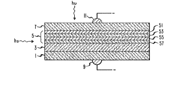
An exemplary embodiment of a strained layer
device according to this invention is depic-ted in
FIG. 1. The particular device depicted is a p-i-n
photodiode, which comprises substrate 1, a first silicon
cladding layer having a first conductivity type 3, a
Gexsil x/Si superlattice region 5 and a second silicon
cladding layer 7 having a second conductivity type. The
se~ond layer and the substrate are electrically
contacted by metalli2ations 9 and 11, respectively. The
substrate also has the first conductivity type~ There
may additionally be a buffer layer between the substrate
and the first silicon layer. The substrate and b~ffer
layer have the same composition and conductivity type.
The superlattice region comprises alternating, that is,
interleaved, layers of Si and Gexsil-x indicated as 51,
53, 55 and 57. More layers will typically be present
but are not shown for reasons of clarity. The region
has a total thickness hSL. Each period has a thickness
T and the Gexsil-x layers have a thickness h. The
layers should be grown in the region of commensurate
epitaxy so that the mismatch strain will not be relieved
by dislocations.
Conventional growth techniques may be used to
fabricate the device including the superlattice region.
Molecular beam epitaxy is conveniently used to grow the
superlattice region as well as the silicon layers.
Details of the growth technique including selection of
-- 6
s~bstrate temperature, layer thickness, etc., are
described in, for example, U.S. Patent No. 4,529,~55
(issued on July 16, 1985 to John C. ~ean,
Leonard C. ~eldman and Anthony T. Fiory). The other
techniques ~sed during fabrication, including, h~t not
limited to, for examp]e, plasma etcning oxidation, oxide
deposition, ion implantation and metallization are
typically standard very large scale integration
processing techniques. As such, they are well known to
those skilled in the art and need not be described in
further detail.
The strained layer region may comprise
alternating layers oE different compositions and lattice
constants. For example, it may comprise interleaved
layers of Gexsil x and GeySil-y with x greater than y
and less than or equal to 1.0 and y greater than or
equal to 0.0 and less than 1Ø The values of x and y
need not be constant within the strained layer region.
Variations of x and y within the strained layer region
may lead to increased waveguiding. The term
superlattice is used to mean the strained layer region
of interleaved Gexsil x and GeySil y layers with x and y
being constant within the strained region.
Due to the shift in bandgap caused by strain,
the choice of x and y, which determines the bandgap,
will be different from that expected from the bandgaps
of the bulk materials. This is illustrated by reference
to FIG. 2 which plots the Ge fraction horizontally
versus the bandgap in eV, vertically for both a strained
and unstrained Gexsil_x/si superlattice. As can be
seen, if the materials were not strained, one would
select x = 0.8 for a photodetector absorbing at 1.35 ~m.
However, because of the shift in band~ap induced by
strain, a value of only approximately 0.3 gives the same
effect. However, because the absorption coefficient
increases rapidly above the bandgap, it is advantageous
for detector efficiency to operate as far above as
possible. For x = 0.3, only marginal sensitivity will
be obtained at l.3 ~m. Similar considerations apply for
other materials and wavelengths.
The substrate had a (100) orientation.
Similar effects are expected for a (110) orientation
while a (111) substrate should yield at most only a
small effect. The orientation of the strain axis
relative to the orientation of the conduction band
minima is critical~
The superlattice, i.e., strained layer region,
is strained because of the lattice mismatch between the
Si and the alloy layers. The thickness of the absorbing
superlattice region may be extended in the vertical
direction without the introduction of additional
defects, e.g., misfit dislocations due to lattice
mismatch arising during the growth process. Light may
be incident on the photodetector vertically or it may be
incident horizontally. In the latter case, the strained
layer superlattice functions as a waveguide because the
Gexsil x alloy layers have an index of refraction
greater than that of Si layers. The latter embodiment
is preferred as the absorbing region is larger than it
is for vertical illumination. Of course, light may be
coupled into the waveguide by means of a grating or a
prism.
Another embodiment of an avalanche
photodetector according to this invention is depicted in
FI~. 3. Numerals identical to those used in FIG. 1
represent identical elements. The device further
comprises a third silicon layer 13 having the first type
conductivity and a thickness ~ and a fourth silicon
làyer 15 having intrinsic conductivity and a thickness
d. The third layer is relatively thin, yenerally less
than lO~~cm, and is depleted during operation by the
applied reverse bias. The device should have a high-lo~
electric field conEiguration, i.e., the absorption and
multiplication regions have a low and high,
-- 8
respectively, electric field. Calculation of
appropriate doping levels will be easily done by those
skilled in the art. The third layer is adjacent the
superlattice region.
Several factors should be considered in the
device design to reduce the excess noise resulting from
the avalanche multiplication process. Electrons should
initiate the avalanche process for the embodiment
depicted. The electric field in the avalanche region
should be near threshold and the avalanche region should
be much thicker than the inverse of the ionization
coefficient. ~dditionally, the electric field in the
superlattice region should not exceed the ionization
threshold for germanium. The resulting electric field
is depicted in FIG~ 4. rrhe field is plotted vertically
and the device regions are shown horizontally. In
another embodiment, the p-n junction is above, rather
than below, the strained layer region. This embodiment
may have better waveguiding properties.
Carriers are absorbed in the superlattice
region and the avalanche process occurs in the intrinsic
conductivity silicon layer. A multiplication factor as
large as 50 was obtained for a breakdown voltage of
~5 volts.
For absorption in the 1.3 ~m region, the alloy
layers in the superlattice region should have a
Ge fraction which should be within the range of
approximately 0.4 to approximately 0.6. It will be
readily appreciated by those skilled in the art that as
x increases, quantum effects may also result in shifts
in the energy levels, ~owever, the thickness of such a
layer is limited to less than approximately 10.0 nm.
For higher values of x and smaller layer thicknesses,
the quantum well shift will be to shorter wavelengths.
It does not therefore pay to increase x above 0.6 since
quantum effects will dominate and 1.3 ~m responsivity
will decrease. Consequently, to ensure that there is
sufficiently large absorption of the incident liyht, the
incident light is conveniently launched into the buried
waveguide formed by the Gexsil-x/si s~perlattice- This
is possible because, as previously explained, the
superlattice has a larger index of refraction in the
alloy layers than in the Si layers.
Yet another embodiment is depicted in FIG~ 5.
This embodiment further comprises a third silicon
layer 21 having the first conductivity type adjacent the
superlattice region 5. There is also a passivation
layer 23. The passivation layer may comprise, for
example, SiO2 and the metallizations, i.e., contacts,
may comprise aluminum. It will be readily appreciated
that the p-n junction may be formed by doping the
epitaxial layers during growth or it may be formed after
growth by using, for example, ion implantation.
For the exemplary embodiment depicted, there
were 20 wells of GeO 6Sio 4, each 4.0 nm thick, which
were separated by 20 nm thick Si barrier layers in the
~ 20 superlattice region. When the Ge fraction increased to
- 0.8, the well thickness had to be reduced to less than
2.0 nm. A waveguide thickness of approximately 6500 ~m
was obtained. The undoped superlattice region was
capped with a 1 ~m thick p-type Si layer doped with
boron at density of approximately 5 x 1016 cm~3 and
capped by a thin p+ contact layer doped to a density of
approximately 1017 cm~3. The electrical characteristics
of the p-i-n photodiode were excellent. The reverse
breakdown voltage varied from 30 to 38 volts regardless
of the Ge fraction in the superlattice. The range for
brea~down voltages was consistent with the silicon
doping level and suggestive of the p-n jùnction within
the Si layer. It was noted that the leakage current
increased slowly with the Ge fraction.
It i~ noted that the device absorbs at
wavelengths as long as approximately 1.55 ~m. This is a
surprising result in view of the expected bandgaps of
-- 10 --
the GeXsil x alloys. It is attributed to the fact that
the amount of strain in the superlattice is large and
greatly reduces the bandgap. Accordingly, the values of
_ selected for the superlattice are reduced from the
values expected to obtain absorption at a yiven
wavelength.
Still other embodiments are contemplated. For
example, the strained layer superlattice may be topped
by an intrinsic conductivity type Ge layer and a heavily
doped Ge layer. These layers together with the
superlattice form an absorption region. ~gain, the
carriers avalanche in the intrinsic conductivity Si
region. Additionally, it will be readily appreciated
that devices other than photodetectors may be usefully
fabricated. For example, it is possible that the
devices may be used as light emitters with the two
cladding layers having opposite conductivity types. The
strain will shift the wavelength of the emitted
radiation fxom that expected from the bulk
characteristics. More generally, devices, such as
MODFETs, in which the transport properties are modified
by stra~l are contemplated. Also contemplated are
heterojunction devices with different bandgaps of which
at least one is modified by strain. It will now be
readily appreciated by those skilled in the art that the
values o x will be reduced in nonoptical heterojunction
devices, such as modulation doped transistors and
heterojunction bipolar transistors. Furthermore, use as
a photodetector at wavelengths between 1.3 ~m and the
silicon band edge is also contemplated.