Note: Descriptions are shown in the official language in which they were submitted.
d ~
- 1 -
RESONANT ï'UNNE,LING DEVICE, ANI:)
MODE OF DEVICE OPF.RAIl[ON
Technical Field
The invention is concerned with apparatus including semiconductor
S devices whose operation is based on resonant ~unneling thrc,ugh a quantum well.
Back~round of the ~vention
Concornitant to a contLnuing trend towards n~iniaturization and
increased functional density in electronic devices, considerable attention has been
paid to so-called resonant-tunneling devices as characterized by operation
10 involving ca~ier energy coinciding with a quandzed energy level in a potential
well. Af~er early theoretical work, resonant-tunneling devices have been
implemented at least experimentally, and an extensive literature has come into
existence concerning theoretical and practical de~,rice aspects as surveyed, e.g., by
F. Capasso et al., "Resonant Tunneling ThIough Double BarIiers,
15 Perpendicular Quantum Transport Phenomena in Superlattices, and l'heir De~iceApplications", IEE~: Journal o~ Quan~u7n Eiectronics, Vol. QE-22 (1986),
pp. 1853-1869.
Resonan~-tunneling devices can be made as diodes and as ~ansistors;
see, e.g.,
E. R. E~rown et al., "Millimeter-band Oscillation~ Based on Resonant
Tunneling in a Double-bamer l:~iode at Room Temperatllre", Applied Pkysics
Le~ers, Vol. 50 (1987), pp. 83-85;
H. Toyoshima et al., "~ew Resonant Tunneling Diode with a Deep
Quantum Well"~ Japan se Jol~rnal of Applied, P*ysics, Vol. 25 tl986), pp. L78
L788;
H. Morkoc et al., "Observation of a Negadve Differenti~l Resistance
Due ~o Tunneling through a Single BalTier into a Quan~um Well", Applied Physics
Letters, Vol 49 (1986), pp. 70-72,
F. Capasso et al., "Resonant Tunneling Transistor wi~ Quantum Well
30 Base and High-energy Injeedon: A New Negative Differential Resistance
Device", Journcll ~Applied Physics, Vol. 58 (19æS~, pp. 136~1368;
N. Yokoyama et al., "A New Functional, Resonant-Tunneling Hot
Elec~on Transistor (RHEI~", Japanese Journal o~Applied Physics, Yol. 24
~1985), pp. L853-L8:54;
- 2 -
F. Capasso et al., "Quantum-well Resonant Tunneling Bipolar
Transistor Operating at Room Temperature", IEE:E Electron Device Le~ters,
Vol. EDI,-7 (1986), pp. 573-575;
T. Futatsugi et al., "A Resonallt-tunneling Bipolar Transistor (RBT):
S A Proposal and Demonstration ~or New Functional Devices with High CulTent
Gains", Technical Digest of the 1986 Internanonal Ælectron Devices Meeting,
pp. 286-2~9;
T. K. Woodward et al., "Experimental Realization of a Resonant
Tunneling Transistor", Applied Physics Letters, Yol. S0 (1987), pp. 451-453;
B. Yinter et al., "Tunneling Transfer ~iel~-effect Transistor: A
~egaeive Transconductance Device", Applied Pkysics l,etters, Yol. 50 (1987),
pp. 410-41~;
A. R. Bonnefoi et al., "Invert~l Base-collec$or Tunnel Transistors",
App~ied Physics Letters, ~ol. 47 (1985), pp. 888-X90;
S. Luryi et al., "Resonan~ Tlmneling of Two~imensional Electrons
through a Quantum Wire: A Negative Transconductance Device", Applied Pkysics
Lette~s, Vol. 47 (1985), pp. 1347-1693; and
S. Lu~yi et al., "Charge Injection Transis~or Based on Real-Space
Hot-Electron Transfer", IEE~E Transac~ions on Elec~ron Devices, Vol. ED-31
20 tl984), pp. ~32-83g.
Considered as of particular interest are devices having cu~ent-voltage
characteristics including mul~ple nega~ve resistance regions - this on a~count of
potentially ~eatly reduced circuit complexity attendant to the use of such devices.
However, while such multiple regions can be obtained ~orn a plurality of
2S resonances of a qualltum well, resulting devices ~ically suffe~ from the
drawback ~lat current peaks corresponding to excited states ca~ry significantly
~eater amounts ~ current as compared with the amount of cu~ent camed in the
ground state.
~ vention
Apparatus in accordance with the invention such as, e.g., central
processors and memory, switching systems, frequency multipliers, and waveform
scramblers include a device which, under suitable operating conditiGns, has a
plurality of negative resistance regions with equal or nearly equal peak culrents,
separation between the peaks being voleage tunable. Device operation is based on35 exclusive use of the ground-state Tesonance of a quantum well. The device
includes a substrate-supported resonant-tunnellng structure be~ween terminals such
~ 3
that side by~side first and third terminals are on one
side, and a second terminal is on the opposite side of
the resonant-tunneling structure.
Included further are (two-terminal) resonant-
tunneling diodes as incorporated in memory devices,
e.g., in lieu of 2-transistor flip-flops; room-
temperature device operation; and devices comprising an
essentially undoped accelerator region between an
emitter contact and a resonant-tunneling structure.
In accordance with one aspect of the invention
there is provided a device comprising a resonant-
tunneling structure, said structure comprising a
quantum-well layer between quantum-barrier layers on a
substrate, with emitter and collector contacts on
opposite sides of said resonant-tunneling structure,
said device further comprising an essentially undoped
accelerator-region layer between said emitter contact
and said resonant-tunneling structure.
Brief Description of the Drawinq
FIGo 1 is a schematic cross-sectional
representation of a pr~ferred embodiment of a device in
apparatus of the invention;
FIG. 2 is a diagram of a circuit which is
operational equivalent to the device shown in FIG. l;
FIG. 3 is a schematic cross-sectional
representation of a second preferred embodiment of a
device in apparatus of the invention;
FIG. ~ is a schematic cross~sectional
representation of a third preferred embodiment of a
device in apparatus of the invention;
FIG. 5 and 6 are photographically recorded
current-voltage diagrams as obtained by operating a
device as shown in FIG. 1;
FIG. 7 is a diagram of first apparatus or
circuit including a device in accordance with the
invention;
FIG. 8 and 9 are schematic current-voltage
- 3a -
diagrams corresponding to operation of a circuit in
accordance with FIG. 7, such circuit serving as a
frequency multiplier;
FIG. 10 is a photographica].ly recorded
current-voltage diagram corresponding to operation of
the circuit shown in FIG. 7, operating conditions being
chosen for waveform scrambling;
FIG~ 11 is a diagram of second apparatus or
circuit including a device in accordance with the
invention;
FIG. 12 is a schematic current-voltage diagram
corresponding to operation of the circuit shown in FIG.
11, such circuit serving as a three-state memory
element;
FIG. 13 is a diagram of a typical integrated
circuit layout using a three-state memory element in
accordance with the invention;
FIG. 14 is a diagram of third apparatus or
circuit including a device in accordance with the
invention;
,
- 4 -
FIG. 15 is a schematic current-voltage diagram corresponding to
operation of the circuit shown in FIG. 14, such circuit seNing as a parity-bit
generator;
FIG. 16 is a diagram of voltage levels representing binary signals in
S pseudo-ternary form as used in coaxial telephone systems;
FIG. 17 is a diagram of fourth apparatus or circuit including a device
in accordance with the invention, adapted ~or coaxial line driving;
FIG. 18 is a current-voltage diagram of an InAlAs-InGaAs-InAlAs
resonant-tunneling diode as opera~ing at a temperat~re of 80 degrees K;
FIG. t9 is a cu~en~-Yoltage diagrarn of an InAlAs-~GaAs-InAlAs
resonant-tunneling diode as operadng at room temperature;
FIG. 20 is a diag~m illustra~ng the effec~ of an accderator region
between emitter con~act and resonant-twnneling structure; and
FIG. 21 is a cu~Tent-voltage diagram of a ~sonant-tunneling device
15 comprising an accelerator region between emitter contaet and resonant-tunneling
structure.
I~etailed Descriptio~
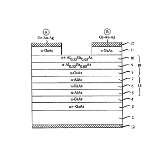
Rep~sentative device s~ucture a~ shown in FI~. 1 may be made by
standard molecular-beam-epitaxy pr~essing star~g with gallium arsenide
20 subs~ate 2 whose crystallogr~phic orientation is (100), and which is doped n+with silicon. Epitaxially deposi~ed on subs~rate 2 is a gallium arsenide buff~
layer 3 which is doped n+ wi~h approximately 5~1017/cm3 silicon, and which has
a thickness of approximately 1 rnieromete~. Fur~her d~stte~i are a nominally
undoped gallium arsenide layer 4 having a dlicknPss of approxima~ely
25 250 nanometers, followed by layers 5, 6, and 7 which form a resonant-tlmneling
double barner 18 including a quantum well. Barrier layers 5 and 7 are nominally
undoped aluminum arsenide layers haYing a thichless of approximately
2 nanvme~s, and quanhlm-well layer 6 is a nominally Imdoped gallium arsenide
layer having a thic~ess of approximately 7 nanometers. (Ba~rier and quantum
30 well layers may have ho nogeneous or heterogeneous composition as, e.g., in the
case of linea~y graded balTier layers or a parabolically g~aded well layer.
Typically, the Ibandgap of the material of ~he quantum-well lay~ is less ~han ~he
bandgap of the mate~ial of the ba~ier layers.)
On the dollble-barlier s~uchlre 18, a heterojunction 1~ is grown,
35 preferably in the form of a modulation-doped aluminum gaLlium arsenide/gallium
arsenide heterojuncdon consisdng OI a nominally undoped gallium arsenide
7~
- 5 -
channel layer 8 having a thickness of approximately 20 nanometers, a norninally
undoped Alo 3~55aO 65As spacer layer 9 having a thickness of approximately
8 nanomete~s, and an A10335GaO 65AS donor layer 10, doped n with
approximately 2xlO /cm silicon, and having a thickness of approxirnately
5 40 nanometers. Channel layer 8 contains a high-mobility çlectron gas which has a
density of approximately 1018/crn3, and which is spatially separated by spacer
layer 9 from the parent donors in the alun~inurn gailium arsenide donor layer 10.
Use of a modulation-doped heterojunction 19 as dessribed above is in
the interest of facilitating the formation of low-resistance ohmic contact to the
10 heterojunction while keeping the dopants away from the double barrier. Also, the
alurr~inum gallium arsenide of layer 9 serves to passivate the adjacent gallium
arsenide channel layer 8.
After deposition of gallium arsenide contact layer 11, doped n~ with
appro~cimately 2xlO171cm3 silicon and having a thickness of approximately
15 140 nanometers, metallizadon layer 12 is formed by evaporation, on layer 11 in
the presence of a lift-oiEf mask, and also on subs~ate 2. Convenien~ly, germanium
~12 nanomete~s), gold (27 nanometers), silver (100 nanometers), and gold
(lSû nanometers) are evaporatecl in succession, and two contact pads A and B aremade approximately 240 micrometers long and 80 }micrometers w~de, situated
20 side-by-side, with long sides adjacent and separa~ed by a distance of
approximately 6.5 micromet~rs. Hea~ treatmen~ ~or 10 sesonds at a temperature of380 degrees C is suitable for alloying of the metallization, and thç alloyed
metallization can filrther serve as a mask for wet chemical etshing of layçr 11 to
expose layer lû, e.g., by means of a selectiv~ s~o~ etch of hydIogen peroxide and
25 ammonium hydroxide, with pH approximately 7.2.
While molecular-beam epitaxy is considered as well-suited and
convenient for device fabrica~ion, the use of other deposition methods is not
precluded. For example, sufficiene accuracy in laye~ composidon and thickness
may be achievable in liquid-phase epi~xy ~PE) and in atomic-layer epitaxy
30 (ALE). Also, while the material system GaAs/AlAs is convenient for device
implementation, other material combinations can be used as selected, e.g., from
the systems ~GaAs/lnAlAs, InGaAsP/InP, and GaAs/AlGaAs, lattice-matched to
suitable gallium-arsenide or indium~phosphide substrates.
With reference to FIG. 2, a dsvice as shown in lF7IG. 1 can be
35 understood in functional ~erms as being equivalen~ to two resonant-tunneling
diodes 21 and 22 in parallel, with resistor 23 connecting the diodes as
Z8
- 6 -
corresponding to the portion of channel layer 8 extending the length of the gap
between contact pads A and B of FIG. 1. (In the device as specifically describedabove, the resistance of this portion as measured between contacts A and B was
~ound to be approximately 12 ohms.) Terminals A and B, as well as substrate
5 temlinal S shown in FI&. 2 are in correspondence with contact pads of FI{3. 1.During device opeMtion, resonant tunneling current flows from the
substrate through the double balrier into the channel layer, and such current flows
under the contact pads as well as in the region between the pads. Preferably,
pads A and B have approximately the sarne area and, for cuITent under the pads to
10 be large, pad area is preferably chosen to significantly exceed the area between
pads. Alternatively, as shown in FIG. 3, layer portions of some or all of layers3 to 10 of FIG. 1 may be etched away bet~ween contacts, leaving, e.g., resonant-tunneling diode s~uctures 31 mutually isolated as may be advantageous in the
interest of minimization of background culTent. F~hermore, etching after layer
15 deposition mav be used to produce, on one and the same substrate, a plurality of
devices in accordance with FIG. 1.
As a fur~her variant form of the device, depicted in FIG. 4, one or
several additional contact pads may be provided be~ween pads A and B of FIG. 1,
~d it is apparent that such provision is functionally equivalent tv the presence in
20 FIG. 2 of rnore than two resonant-tunneling diodes in parallel. In this case, the
resistance of por~ions of layer 8 extending betweerl contact pads conveni~ndy
provides for voltage division, ~ereby obviating the need for addidonal voltage
sources. (In the interest of appro7cimately constant voltage division, design of ~he
s~ucture preferably providos for sufflciently large cu~ent in the divider network
25 as compared with current through the resonant-tunneling dlodes.~
Further wi~h reference ~o FM. 1, device operation equivalent to side-
by-side resonant-tunnelin~ diodes can be realized also in thc absence of
heterojunction 19, in which case an offset layer may be used replacing
heterojunction 19; for example, a S-nanometer layer of undoped gallium arsenide
30 is suitable for this purpose.
While it is possible to implement the circuit of FIG. 2 using discrete
tunnel diodes 21 and 22, a monolithically integrated device has disdnct advantages
in that, e.g., parasitic resistances and capacitances are reduced, and in that the
reproducibil;~ of cuIrent-voltage characteristics is enhanced due tO uniformity of
35 dop~r~g levels in ~he two or more resnnant-turmeling diodes made on a ~ommon
substrate in the course of one and the same manufacturing prosess.
- 7 -
For different values of the potential difference VBA be~veen terminals
B and A of FIC3. 1, current through substrate terminal S of a device as described
above was measured as a fun tion of a positive bias applied between tenninal S
and grounded terminal A, this culTent is essentially the sum of the two resonant-
S tunneling cu~ents flowing through the two resonant-tulmeling diodes. As is
apparent upon inspection of the corresponding graphs (FIG. S and FIG. 6), for
zero potential difference YBA there is a single cu~ent peak, negadve conduc~ancebeing due to quenching of resonant h~nneling through the clouble barriers under
te~ninals A and lB. When terminal B is biased negatively with respect ~o
10 terminal A (FIG. 5), an additional cu~ent peak develops at lower voltages; the
position of one peak remains unchanged while ~hat of the oth~ moves to lower
bias as the potential difference VBA between 3E3 and A is made more negative. Byappropriate choice of the bias between B and A the two peak currents can be
made nearly equal.
An explanation of this effect may be pro~ided as follvws: As a IeSlllt
of the bias applied between A and B, the potential differences a~oss the two
double barliers are dif~elen~, and for B negatively biased wi~h resp~t to A,
resonant tunneling ~rough the douUi banier unde~ terminal B is quenched at a
lower subst~ate bias than in the double barner unde~ tem~inal A, leading to two
20 peaks in the curxent-vol~a~ diagram. The peak ~hat does not shift with
varying VBA is associated with ~enching of resonant tulmeling th~ough ~he diode
under teIminal A. As exp~ted, the separation be~ween the peaks is nearly equal
to the bias applied betweell A and B.
Finally, if ten;ninal B is positively biased with respect to te~minal A
25 (FIG. 6~, a higher voltage is regui~ed to quench resonant tunneling ~hrough ~he
double barIier under terminal B, leading to a second pealc which shifts to higher
voltages as VB ,9, is increased. Similar results are obtained with negative biasapplied to te~n~inal S.
While the characte~stics of FIG. S and 6 were obtained ~or an
30 operating tempera~e ~100 K, suitable prwessing and material choices are
expeceed to perrnit room-~emperature device opçration as have been realized in
resonant-tlmneling diodes and transistors.
The device of F~G. 1 can be used in suitably designed circui~y for a
vanety of fimctions; one circuit, designed for fireqllerlcy multiplica~on, is shown
35 ill PIG. 7 wi~h associated cu~ent-voltage diagrarns of F;IG. 8 and ~IG. 9, bias
voltage VB,~ between te~minal A and B of the device being fixed.
7'~.
FIG. 7 shows device 1 with terrninals A, E'., and S in accordansc with
FIG. 1, source 51 of substrate bias voltage Vss, source 52 of bias voltage VBA,
input signal source 53, resistor 54, and output ~erminals 55.
F~G. 8 shows device characteristics in the case of a sawtooth input
5 voltage, substrate bias voltage Vss having been adjusted to select the quiescent
operating poin~ A~. As the sawtooth input voltage increases from Al to Bl, the
operating point s'ni~ts from A2 to B2 along the charactelistic, with the subs~rate
culTent Is increasing approximately linearly. ~he output voltage across tne
resistance R is proportional to the svurce cu~ent Is, and ~hus its increase from A3
10 to B3 is also approxinately linear. As th~ input voltage increases 'oeyond Bl, the
source culTent Is suddenly drops to the valley point B~', resuldng in a sudden
drop in tne output voltage from B3 to B3'. Between B3 and C3, the output
condnues ~o rise again, followed by a second drop at C2, and then a rise as the
input continues to rise up to Dl. At Dl, ~he input returns to ~ero to start a new
15 cycle, and the operating point also shifts back to A2, with a drop in the output as
well. Accordingly, the frequency of tne sawtooth input signal has been multiplied
by a factor of 3. (If YBA had been adjusted to produce a single peak in the
cu~rent-volta~e diagram, saw~oosh frequency would have been multiplied by a
factor of two.)
2() FIG. ~ illus~ra~es device operation in case of a sine-wave input and is
amenable to detail~ descnption analogous to desaiption in the case of FIG. 8
abl)Ye. The output waveform is found to be rich in the fifth haImonic of the
input. ~l[f VlBA had been adjusted to produce a single peak in the cunent-voltage
diagram, the outpu~ would have been rich in the third haImonic.)
Expe~ental resul~s obtained with VBA=lY and VSS=2.3Y in the
circuit of FIG. 7 showed superior efficiency in frequency multiplication and in
generating fifth harmonic as compared with ~onventional devices such as, e.g., astep re~ov~ry diode.
FIG. 10 shows output of a circuit of FIG. 7 used for waveform
30 scrambling in the case of a sine-wave input signal. Scramblilg is effected bychoosing a bias VBA such that the two cunent peaks are of different height (here,
specifically, VBA=1.4V) in which case the input wavçform is broken up at
arbit~lary phases, and the different segments are amplified differently at the ou~put.
The original waYefonn can be recovered from the scrambled signal by using an
35 identical device in the feedback circuit of an amplifier, biased to the same voltages
as in the scrambling circui~
FIG. 11 shows a circuit which can serve as a mernory element in a 3-
sta~e logic system. Shown are source 91 of supply voltage Vss, source 92 of biasvoltage VBA, input signal source 93, resistor 94, and output term~nal 95. As
illustrated in FIG. 12, the bias voltage V~A between the terminals A and B is
S adjusted ~o produce a curren~-voltage characteristic having essentially equal peaks
at the same culTent level. And, for a suitable supply voltage V~s, and load
resistance RL, the load line intersçcts the current-voltage characteristic at five
different poin~s of which three (Ql~ Q2~ and Q3) are in the positive slope par~s of
the curve and hence correspond to stable operating points. Corresponding to these
10 stable operating points there are respective output voltages ~1~ V2, and Y3, and
the circuit can stay indefinitely at any one of these points, thus retaining the last
voltage infolmation supplied. Thus, the device can be used as a memory element
having three stable states, with voltages Vl, V2, and Y3 representing three logic
values. (As compared with exis~ing three-ssate logic circuits requ~ring 4
15 conventional transistors and 6 resistors, this represents a significantly simple~
alternative.) The circuit can be switched from one s~ate to another by applying a
short voltage pulse.
In an experiment, switching between states was effected by
momentarily changing the supply voltage YSs which is equivalent to applying a
20 short voltage pulse. With a supply voltage vss=l6~r~ a load resistance
RL=215 ohms, and a bias voltage VBA=0.7V, the three stable states wer~ found
~o be at 3.0V, 3.6V, and 4.3V. The cor~esponding load line as drawn on the
measured cu~n~-voltage charactelis~s OI the device intersects, respectively, at
2.8V, 3.4V, and 4.1V, in close agreement with ~e measured values of thc
25 operating points.
171e threc-state memory cell as discussed above in connection with
FIG. 11 and FIG. 12 is well-suited for integradon in memo~y integrated circuits
with read-wT~te and encoding capabili~es as shown in m~. 13. The memory cells
are interconnected as a ma~ix a~ray, and a par~icular element in the alray is
30 addressed by ac~ating the corrcsponding row- and column-select lines. A ~ow-
select connects each device in a specified row to the co~esponding column line,
and the column-selec~ connects the selected column to the data bus. For example,in ~hs case OI the (i, j)-element shown in FIG. 13, when the i-th row-select line is
acdvated, dle driving switch Ql is turned on, as well as the switches for eve~y
35 element in the i-th row. The column-select logic now connects the j-th column tO
the data bus. l~e temary idendty cell T (described in detail, e.g., by A. Hcung
~z~
- 10 -
et al., "An all-CMOS Ternaly Identity (:ell for VLSI Implementation", Electronics
retters~ Vol. 20 (lg84), pp. 221-222) acts as buffer between the memory element
and the extel~al circuit. For reading data from the memory, the identi~ cell is
activated with the read-enable line, and data from the (i, j)-th element is
5 transferred via the data bus to the VO pin of the c~rcuit. When the write-enable
line is activated, data from an external circuit is connected to the data bus and
written on the (i, j)-th element.
FIG. 14 shows a circuit which can operate as a 4-bi~ parity generator,
appreciation of corresponding device operation being facilitated by reference tolû FIG. 15 which shows the current-voltage characteristic of the device. The four
digital input signals are added in the inverting summing amplifier Al to producefive distinct vol~age steps at its output, co~esponding to the number of digital bits
in the high state. Normally, ~he output of A1 would be negative for positive input
voltages. The addition of a suitable negative offse~ voltage V~l;F at the input
1~ results in up-shifting of the waveform to produce the output fs~r Al shown in the
bottom part of Fl{;. 15. The subst~ate bias voltage Vss is adjusted to select the
opera~ng poînts of the device at the five points emphasized by dots in the
current-voltage charactenstic, corresponding, respectively, to the five voltage
levels at the Al output. The substrate cuIrent of the device generates a voltage20 across the 7.5-ohm resistor, which is picked up by the buf~er amplifier A2. The
circui~ operates as a 4-bit parity generator in tha~ its output is high when ~e
mlmber of input bits set high is odd, and low otherwise. As compared with a
conventional circuit usLn~ 3 exclusive-OR gates, each requiring 8 transistors,
considerable reduction in the number of cir~uit components is lealized in the
25 circuit of FIG. 14.
While implementation of circuits o~ FIG. 7, 11, 13, and 14 pre~eIably
involves the use of highly miniaturized resonant-~unneling devices, relatively
large-scale devices having dimensions as described with respect to FIG. 1 are ofirnrnediate interest on account of low internal impedance of approxima~ely
30 10 ohms, and further on account of compatibility wi~h bipolar threshold detectors
due to voltage steps of approximately 0.6 to 0.7 volts. In view of such impedance
and vol~age characteris~ics, a device as descnbed can be used as a driver of thepseudo-ternary signal used in coaxial-cable telephone transmission; see FIG. l6
for a typical such signal stream as designed for easy ex~acdon of the clock signal.
FICJ. 17 diagrammatically shows pseudo ternary driver 71 for coaxial
cable 72; driver 71 includes device 1 in accordance with FIG. 1. Preferably,
internal impedance of driver 71, as observed from cable 72, is less than
approximately one-tenth of the characteristic impedance of cable 72, the latter
S typically being in the range from 50 to 75 ohms. Nonnally, the dIiver is at the
middle state (M-state). ~ an up-going pulse 73 is applied, the driver undergoes
transition to the high state (H-state), and if then a down-going pulse 74 is applied,
the driver Tetums to the middle state. With the driver at middle state, if a down-
going pulse 74 is appli~d, the drivçr swi~ches to the low state (L-state).
Among advantages of a driver as described are fast switching speed
and small current spike as there is no overlapped drive due to signal skew.
As the three-terminal device described above is operationally
equivalent to a circuit comprising resonant-tunnelillg diodes in parallel, attention
may be directed to resonant-tunneling diodes individually, i.e., as two-terminal15 devices. Moreover, as also sta~ed above, room-temperature operation of ~two- or
mul~-terminal) dev~ces is desirable. In these re~pects, and f lrther to the device
descnbed above, a tw~terminal device is of inteTest as exemplified by a device
made by molecular-beam epi~cy processing as follows:
On an n+ indium phosphide subs~ate a one-micromete~ buffer layer
20 was growll of n~ (appro~ately 3 x 10¹⁷/cm3~ GaO 471no 53As, followed by a
resonant-~unneling struch~ consis~ng of ~hree 5-nanomete~ layers such as ~ firstbarrier layer of undoped Alo 48~t~ 52As, a quantum well layer of undoped
Ga0 ~7~0 53As, and a second barrier layer of undoped Al$.4gIn0 52As. On the
resonant-hJnneling struch~ret a l~micrometer cap layer of n (app~oximately
2~ 3 x 10¹⁷/cm3) ~a~ 47In0 53As was deposited.
A 5~micrometer mesa structure was folmed by etchin~
I H2O2 + 3 H3PO~ + SQ lE~2O at room temperatu~e, and a top ohmic con~act
ha~ing a diameter of 30 micrometers was made by sequential deposition of
6 nanometers gelmanium, 13.5 nanome~ers gold, 50 nanor~ters silver, and
30 75 nanometers gold, and alloying at a tempela~ure of 420 degrees C for
30 seconds. For ~he bottom contact, 5 nanometers nickel, 385 nanome2ers gold,
21.5 nanometers gerrnanium, and 75 nanometers gold were depos;ted on the
etched sufface of the buffer layer and alloyed at a temperature of 420 degrees C~or 30 seconds.
- 12 -
Diode operation was tested at a temperature of 80 degrees K and at
room temperature in a Heli~ran dewar equipped with n~icroprobes. Resulting
current-voltage characteristic are as shown in PIG. 18 and FIG. 19, respectively,
bias voltage being defined as volta~e of the top contact relative to the bottom
S contact. As can be seen from FIG. 19, room-temperature operation exhibits a
peak-to-valley ratio of 4: 1 in one polarity, and 3.5: 1 in the other. While thepeak-to-valley ratio increases upon cooling of the device, pealc culTent remainsessentially constant (approximately 125 mA at 600 mV).
An electlon-tunneling-transmission calculation shows that the first
10 resonance is at El = 126 meV f~om the bottom of the quantum well. Appearance
of the peak in the clurent-voltage chaTacteTistic at a voltage greater than
2 lEl/e = 252 mV may be explained by consideration of the voltage drop in the
depletion and accumulation regions in the collector and emiKer layers adjacent to
the double-barrier. Thus, to line up the first su~band in the well wi~h the bottom
15 of the conduction band in the emitter ~and thus to guench resonant tunneling), a
larger voltage is required across the entire stmcture. On accmmt ~ large peak-
t~valley ratio as obsen~ed ae operating ~empeTatures }~igher than ~hose previously
employed, a resonant-tunneling diode as descAbed above is suitable fo~ operationat ~emperatlllres greater than 100 degrees K and, in particular, at temperatures at or
20 near room temperature.
On account of bist~bility, resonant-tunnelillg diodes are suitable for a
variety of circuit applications. For example, a circut~ consisting of a voltage
source, a resonan~-tunnelinp diode, and a load ~esistor in se~ies can serve as abistable memory cell as ma~r be implemented, e.g., by repla¢ing device 1 in
25 FIG. 13 by a ~esonant-~unneling diode. (The above-desc~ibed resonant-tunneling
- diode, in series wi~ a 30-ohm load resist~r and a 3-volt power supply, was found
to have room-~emperatl re operating points at 0.47 '~1 and 0.85 V.) ~ue to the
greate~ simplici~ of resonant-tunneling diode cells as compared with
conventlonal, ~-~ransistor flip-flop circuit cells, integration R resonant-tunneling
30 cliode cells ineo me}nor~Y arrays may require ~ewer in~erconnections.
As can be seen from FIG. 18 and 199 the diode as described above
exhibits abrupt current drop. While this devlce aspect is desirable, e.g., for
memory applications, other devtce uses such as, e.g., analog applications may
preferably be based on charactenstics haYing a region of more ~radual current
35 transition. A device of this latter kind has been realized as follows: on theemitter side of the device, an essen~ally undoped layer is inte~osed between the
34~
contact and the first barrier layer to permi~, during device operation, ernittedcamers to be accelerated in the electric field in the undoped layer. As a result,
carrier energy at the ba~rier can be described by a distribution as depicted in the
diagram of FIG. 20, with a peak occu~ing at an energy substantially higher than
5 the conduction band edge. Depending on bias voltage, carriers to either side of
the energy peak are available for resonant tunneling, as a result, instead of abrupt
quenching, the resonant-tunneling current drops gradually beyond the peak
voltage. In the interest of an appreciable effect, prefeIred accelerator layer
thickness is greater than or equal to 40 nanometers.
Shown in FIG. 21 is the current-voltage characteristic of a
coIresponding device having the followillg specifi~ struchlre on an indium
phosphide su~stra~e: 500 nanometers n+ GaO 47In~ 53As, S nanometers undoped
Alo 48In0 5~As, 5 nanometers undoped GaO 471nO 53As, S nanometers undoped
Alo 4~InO 52AS, 2~3 nans~meters undoped GaO 47InO~53As, and 200 nanometeIs
15 n ~aO.47In0.53AS-