Note: Descriptions are shown in the official language in which they were submitted.
SEMICONDUCTOR DE~ICFS EMPLOYING HIGH RESISTIVITY
In-P BAS~ PITAXIAL LAYF,R FOR CURRENT CONFINEMENT
Back~round of the Invelltion
This invention relates to a vapor phase epitaxial growth technique
5 utilized to fabricate semiconductor devices such as light emitting devices, light
detecting devices, and field-effect transistors.
A comn1on problem in the fabrication of low threshold buried
heterostructure (BH) lasers in the InGaAsP/InP materials system is the control of
leakage currents (i.e., currents which bypass the active region of the device).
1() These currents lead to high lasing threshold, low differential quantum efficiency,
abnormal temperature dependence of threshold current, and rollover of the light-current (L-I) characteristic. All of these factors have a significant negative impact
on the use of BH lasers in transmitters for fiber optic comrnunication systems.
One possible solution to the problem o leakage current in buried
15 heterostructure lasers is the controlled introduction of high resistivity material into
the device structure. This high resistivity material could be used to block current
flow through undesired leakage paths. Previously, high resistivity liquid phase
epitaxial (LPE~ Al0 65(:;aO.3sAs (lightly C;e-doped) material has been utilized for
current confinement in AlGaAs/GaAs buried heteros~ructure lasers, but subsequent20 attempts to produce high resistivity LPE InP material for this purpose have not
been successful. Deuteron bombardrnent has also been shown to prodoce highly
resistive material from p-type InP, bu~ this material is not expected to remain
highly resistive during subse~quent processing. In particular, because the high
resistivity is related to deuteron implant damage, the resistivity anneals out at the
25 high temperatures (e.g., above about 6(30C~ required for subsequent LPE growth.
In addition, lbiffircated, reverse-biased p-n junctions haYe also been
reported for constraining current to flow through the active region of InGaAsP/InP
lasers. These blocking junctions have been fabricated by the implantation of Be
into n-InP substrates, by the diffusion of Cd into n-InP substrates, and by the
30 epitaxial growth of a p-InP layer onto an n-InP substrate. But, all of these devices
are impaired to some extent by leakage currents because of the imperfect blocking
charactenstics of the reverse-biased junctions.
More recently, D. P. Wilt et al. reported in Applied Physics Letters,
Vol. 44, No. 3, p. 290 tFeb. 1984) that ~P/InGaAsP CSBH lasers with relatively
35 low leakage cuIrellts and low lasing thresholds can be fabricated by incorporating
into the structure a high resistivity Fe-ion-implanted layer which constrains
pumping current to flow through the active region. The high resistivity layer is
prod~lced by an Fe-ion implant into an n-type InP substrate followed by an
annealing treatment prior to LPE growth. Although the resistivity of the Fe-ion-implanted layer is stable even after being subjected to the high temperatures
charaGteristic of LPE growth, the thinness of the Fe-implanted layer (about
5 0.4 ~Lm) renders it difficult to reproducibly position the thin active layer (about
0.1-0.2 !lm thick) adjacent thereto~ When the active layer is not so placed, shunt
paths are created which allow leakage current to flow around the active layer.
Hence, high performance (low threshold, high efficiency) devices are hard to
fabricate reproducibly.
Others in the prior art have attempted to utilize hydride vapor phase
epita7sy (VPE) to grow high resistivity Fe-doped InP, but this approach has been a
difficult task because suitable volatile iron compounds typically cannot be
transported using a hydrogen carrier gas at temperatures normally used for growth
(e.g., T ~ 650C). The growth of InP in an inert carrier gas is difficult as well
15 and has been reported only for a trichloride system (using PCl3) when PH3 wasadded to stimulate growth. See P. E. Giles et al., Journal of Crystal Growth,
Vol. 61, p. 695 (19~3).
Summary oï tlhe Invention
In accordance with one aspect of our invention, a method of
20 fabricating a device, which includes an iron-doped, indium-based, compound
Group III-V semiconductor region, comprises the steps of (1) forrning a precursor
gas comprising a carrier gas, a volatile dopant compound, a volatile indium
compound and a Group V hydride, (2) directing the precursor gas through a
heated chamber to contact a heated deposition body, and (3) inducing deposition
25 of the compound semiconductor on the body, cbaracterizsd in that the caIrier gas
comprises an inert gas, the dopant compound includes iron, the concentration of
hydrogen in the precursor gas is limited to prevent excessive precip;tation of iron,
and the concentrations of said volatile indium compound at the body and of the
hydride are main~ained sufficient to result in deposition of the semiconductor.
In one embodiment, a semi-insulating, iron-doped, InP-based,
compound Group III-~ semiconductor region is fabricated by using a precursor
gas comprising a nitrogen carrier, E;eCl2, InCl and PH3, and the concentration of
hydrogen in the precursor gas is limited by limiting the amount of pyrolysis of
PH3. This process is capable of producing a region having a resistivity greater
35 than 108 Q-cm which is suitable for use as a current-blocking region in a number
of devices, e.g., light emi~ting devices, light detecting devices and FETs.
~Lf~2
Brief Desc_ption of the Drawin~
The invention, together with its various features and advantages, can
be readily understood from the following, more detailed description taken in
conjunction with the accompanying drawing, in which, in the interests of clarity,
5 the figures have not been drawn to scale:
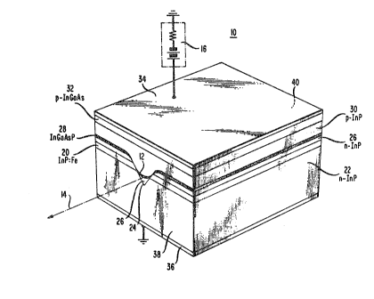
FIG. 1 is an isometric view of a CSBH light emitting clevice
fabricated in accordance with one embodiment of the invention;
FIG. 2 is an end view of another CSBH device fabricated in
accordance with another embodiment of the invention; and
FI~:;. 3 is an end view of a DC-PBH device -fabricated in accordance
with still another embodiment of ~he invention.
I~etailed Description
The semiconductor light emitting device shown in FIG. 1 may be used
as a laser or as an edge-emitting LED. In either case, the device 10 includes an15 active region 12 in which the recombination of electrons and holes causes
radiation to be emitted at a wavelength characteristic of the bandgap of the
semiconductor material of the active region (e.g, about 1.0-1.65 ,um for InGaAsPdepending on the specific composition of the alloy). The radiadon is directed
generally along axis 14 and is primarily stirnulated emission in the case of a laser
20 and primarily spontaneous emission in the case of an LED.
This recombination radiation is generated by forward-biasing a
p-n junction which causes minority carriers to be injected into the active region.
Source 16, illustratively depicted as a battery in series with a current-limiting
resistor, supplies the forward bias voltage and, in addi~ion, provides pumping
25 current at a level commensurate with the desired optical output power. In a laser,
~he plmlping current exceeds the lasing current threshold.
In general, the devic~ includes means for constraining the pumping
current to How in a relatively naIrow channel through the active region 12. As
illustrated, this constraining means comprises a bifurcated, high resistivity
30 Fe-doped InP epitaxial layer 20, and the active region 12 has the shape of a stripe
which lies in the rectangular opening (top view) of the bifurcated layer 20. Note,
in the case of a surface emit~ing LED the layer 20, rather than being bifurcated,
might take the shape of an annulus surrounding a cylindrical or mesa-like activeregion.
The structure shown in FIG. 1 is known as a channeled-substrate
buried heterostructure (CSBH) laser which includes an n-InP substrate 22 and an
Fe-doped high resistivity InP epitaxial layer 20 which is bifurcated by a
groove 24. The groove is etched or otherwise formed through layer 20 into
substrate 22. A preferred technique for controllably etching the groove in the
shape of a V is described in U.S. Patent No. 4,595,454.
The following essentially lattice-matched epitaxial layers are then
5 epitaxially grown on the etchecl wafer: an n-InP first cladding layer 2~ (the
central portion of which fills at least the bottom portion of groove 24); an
unintentionally doped InGaAsP layer 28; a p-InP second cladding layer 30; and a
p-InGaAs (or p-InGaAsP) contact-facilitating layer 32. Layer 28 includes
crescent-shaped active region 12 which, in practice, becomes separated from the
10 remainder of layer 28 because epitaxial growth does not take place along the top
edges of the groove 24. Provided that nonradiative recombination at the interface
with high resistivity layer 20 is not significant, the actiYe layer is preferably
vertically positioned within the thickness of the high resistivity layer 20 in order
to reduce leakage current. However, if the active layer is below layer 20, but near
15 enough thereto (i.e., < 1 ~Im away), leakage currents are still significantly reduced
and nonradiative recombination at the layer 20 interface becomes much less of a
problem.
Altllough the high resistivity InP:Fe layer 20 is forrned direcdy on the
subs~rate 22, it may also be formed on an epitaxial buffer layer (not shown) grown
20 on the substrate. For CS~H InP/lnGaAsP lasers a resistivity in excess of about
1 x 10⁶ Q-cm is desirable. In either case, this aspect of the invention utili~es the
growth of high resistivity InP:Fe layer 20 using hydride VPE with N2 as an inertcarrier under condi~ions of limited PH3 pyrolysis in the reactor. By using an inert
carrier and limiting ~he presence of H2 to that formed by the reaction of HCl with
25 In~l~ and Fe(s) and the pyrolysis of PH3, the invention achieved transport ofsufficient FeCl2 (and hence limited the excessive precipitation of iron by
hydrogen) to produce InP:Fe with a resistivity of > 108 52-crn.
A high resistivity layer prepared by this hydride VPE process
maintains its high resist-ivity even after being subjected to the high temperatures of
30 subsequent process (e.g., LPE) steps.
Electrical contact is made to the device via metal electrodes 34 and 36
on layer 32 and substrate 22, respectively. Source 16 is connected across
electrodes 34 and 36.
Although a broad-area contact is depicted in FIG. 1 by layer 3~ and
35 electrode 34, it also is possible to delineate a stripe geometry contact as shown in
FIG. 2. Here components with primed notation in FIG. 2 correspond to those
2~3'7~
with the same reference numerals in FIG. 1. Thus, the contact-facilitating
layer 32' is etched to -form a stripe and is aligned within the stripe-shaped opening
of SiO2 layer 33. A stripe-shaped metal contact 35 is formed on layer 32' in theopening of SiO2 layer 33, and a broad area electrode 34' is then formed over the5 top of the device. A contact configuration of ~his type reduces device capacitance
and hence increases high speed performance.
The CSBH laser also includes means for providing optical feedback of
the stirnulated emission, typically a pair of separated, parallel, cleaved facets 38
and 40 which form an optical cavity resonator as shown in FIG. 1. The optical
10 axis of the resonator and the elongated direction of the stripe-shaped activeregion 1~ are generally parallel to one another. Other feedback techniques are
also suitable, however, including well-known distributed feedback gralings, for
example.
This example describes the fabrication of high resistivity InP:Fe
15 epitaxial layers by a hydride VPE process. These high resistivity layers can be
incorporated into CSBH lasers (as described above) as well as into other device
structures as desc~ibed hereinafter. The various materials, dimensions,
concentrations, etc., are given by way of illustration only and are not intended to
limit the scope of the invention unless otherwise stated.
The reactor used for the growth of the InP.Fe is described by
R. F. Karlicek et al. in Journal of Applied Physics, Vol. 60, p. 794 (1986). Thesource gases included HCl and PH3 mixtures (5% aud 2%, respectively) in ul~ra
high purity N2~, and the N2 carrier gas ~99.999% pure) was obtained from a
standard compressed gas cylinder. The concentration ot the input reactive gases
25 was selected using electronic mass flow controllers. The ~ransport of iron as the
dichloride FeCl2 was accomplished by flowing HCl (5% in N2) ~rough iron
powder (99.999% pure) placed on a quartz frit which was located downstrcam of
the In~) source in the reactor source region. The In(l) source ~emperature, the Fe
source temperature, and the growth temperature were kept constant at about
30 700C. Between growth experiments, Pd-purified H2 was made to flow through
the reactor in place of N2-
Using an optical spectrometer which monitored the wavelength regionbetween 200 and 330 nm, the extent of PH3 pyrolysis was deterrnined by
measuring the absorbance by P4 a~ 230 nm. Since P4 is the dominant species
35 (except for unpyrolyzed PH3), the concentration of P2 was not monitored optically
and was not included in the compu~ation of the degree of PH3 pyrolysis d~ing
growth. The transport of FeCl2 was also monitored optically, and the
concentration was computed from published thermodynamic data for the Fe-Cl
system.
As noted ~arlier, by using an inert carrier gas and limiting the
presence of hydrogen to that folmed by the reaction of HCl with liquid indium
5 and solid iron and by the pyrolysis of phosphine, the invention achieve su-fficient
transport of FeCl~ (and hence limited the excessive precipitation of iron by
hydrogen) to produce InP:Fe with a resistivity of > 10~ Q-crn.
The growth of InP:Fe was performed on <100> oriented InP:S
substrates which were degreased prior to placement in the reactor. Following the10 preheating of the substrate under a dilute PH3 flow, a brief etch was performed by
initiating the flow of HCI through the Fe source. Growth was initiated by starting
the flow of HCl over the In(l) source region. The specific growth conditions were
as ~llows: PH3 pressure of 17.9 x 10⁻³ atm, InCl pressure of 4.0 x 10⁻³ atm,
HCl pressure of 0.1 x 10⁻³ atm, and total flow of 2250 sccm. The combination of
15 the iner~ carrier gas (e.g., N2), the volatile dopant compound (e.g., FeCl2), the
volatile indium compound (e.g., InCl) and the Group V hydride (e.g., PH3) are
known as a precursor gas. These conditions produced in InP:Fe growth rates of
16 ~lm/hr. The resulting InP:Fe layer was measured to have a resistivity of about
2.4 x 10~ cm.
In addition, the invention contemplates the ability to grow by hydride
VPE InP-based epitaxial layers having the physical characteristics (e.g.,
resistivities of > 106 Q-cm and thicknesses of > 1 ,um) of Fe-doped InP-based
layers grown by MOCVD. These InP-based layers include, for example, In&aP,
InAsP, InGaAsP and InGaAlP.
Moreover, while the invention has been discussed with reference to
lasers and LEDs, it will be appreciated by those skilled in the art that it is
applicable to other semiconductor devices (e.g., photodiodes, FE3Ts) in which
substantial current is prevented from 9Owing through a region of the device.
One alternative laser structure which may be fabricated in accordance
30 with the invention is known as the double channel planar buried heterostructllre
(DCPBH). The conventional DCPBH laser is described generally by I. Mito et al.
in Journal of Lightwave l'echnology, Vol. LT-l, No. 1, p. 195 (1983). It employsLPI3 re~rowth in the channels to form reverse-biased blocking junctions which
constrain current to flow through the elongated mesa containing the active layer.
35 In accordance with a DCPBH embodiment of the invention shown in FIG. 3,
however, the LPE regrowth of blocking junctions is replaced by growth of InP:Fe
~ 7 ~ ;;~ "~
zones 40 on each side of the mesa. A restricted (e.g., stripe geometry) contact 42
is delineated on top of the mesa by a patterned dielectric ]ayer 44 (e.g., SiO2) and
an electrode 46 overlays the top of the device. In this fashion, current is
constrained by the InP:Fe zones 40 and the dielectric layer 44 to flow essentially
5 only through the mesa and hence through the active layer 50.
Finally, it is well known that the active region of the devices
described above rnay include a single active layer or a composite of several layers
at least one of which is active (in the light-emitting sense). Thus, in a 1.55 ~,lm
InP/InGaAsP laser, the active region may include an InGaAsP layer which emits
10 light at 1.55 llrn adjacent another In~aAsP layer (~ = 1.3 ~m) which serves an
anti-meltback function during l,PE growth. Moreover, several active layers
em~tting at different wavelengths are also embraced within the definition of an
actlve region.