Note: Descriptions are shown in the official language in which they were submitted.
16
~ATA COL I~CrlNG SYS~:M
sackpround Or the Invention
F d of the Invention
This invention generally relates to a data collectin~ system and more
particularly to a system accordin~ to which portable data collectors are
carried by the users to collect the data, and the data is transEerred to a
central pr~cessing unit so as to be processed and stored therein.
(ii) Description of the Prior Art
A conventional data collecting system consists of connectin~ portable data
collectors directly to a central processing unit via a communication line, in
order to transmit and receive the data.
In the conventional data collecting system, however, the portable data
collectors are provided with an interface circuit that connects to the host
computer. Furthsr, the interfaces that connect to the central processing unit
require an interface circuit or a connector that meets the ratings such as
EIA RS 232C or RS 422, making it difficult to reduce the size and weight or to
make the device moisture-proof. ~oreover, the data collectors are used at all
times being powered by a cell. To restrain the consumption of current by the
circuits, therefore, it is not feasible to use clock si~nals of a high
frequency, and the transmission speed of the interfaces is at most 9600 bps.
Furthermore, the connector which is attached and detached repetitîvely loses
its reliability. Moreover, since the data is transferred in a one-to-one
manner between the portable data collector and the host computer, one of the
portable data collectors occupies the central processing unit, and other
portable data collectors must wait for their turns. Therefore, the efficiency
of data transfer is very poor.
Even if the host computer transfers the same data which requires a long
time for trans~er to a plurality of portable data collectors, the central
processing unit has to transfer the data to each portable data collector
sequentially, and so it causes a waste of time.
Summary of the Invention
It is therefore an object of this invention to provide a system which
exhibits a high transmission speed relative to the host computer. It is
PAT 10342-1
3321~
another object of this invention to provide a portable data collector which is
small ln size, light in weight, and which is moisture-proof.
It is a further object of the invention to provide a system which consumes
low electric power.
According to this invention there is provided a system for collection of
data and entry of the data to a host computer wherein the system comprises a
portable, hand held data collector for colleçting data and a stationary data
relay for receiving the data from the data collector and for transmitting the
data to a host computer. The portable hand held data collector includes a
case of a size and sh~pe to be held by one hand during use, a keyboard for
inputting the data, display means for displaying the data, memory means for
storing the data and interface means for transmitting the data externally to
the data collector. The data relay includes a case shaped to set the portable
data collector thereon, first interface means for receiving said data
transmitted from the data collector and second interface means for
communicating bi-directionally to the host computer.
It is especially advantageous that the interface means in the data
collector and the first interface meanq in the data relay have respective
circuit means for transmitting the data bi-directionally using electromagnetic
induction. Each of these circuit means comprises a tuning unit having a coil,
and a capacitor connected in parallel with the coil for generating an
electromagnetic field when data are transmitted and for generating an electric
signal by electromagnetic induction when data are received, a transmitting
unit for inputtlng an electric signal to the tuning unit when data are
transmitted, and a receiving unit for outputting the electric signal generated
in the tuning unit as serial data, the transmitting unit and the receiving
unit being coupled together through a capacitor.
Br~ef Description of the Drawin~s
3~ Fig. 1 is a diagram showing the overall structure of a data collecting
system according to the present invention:
Fig. 2 is a perspective view of a portable data collector and a data relay;
Figs. 3, 4 and S are sectional views of major portions of the data relay
according to the present invention:
Fig. 6 is a block diagram of the data relay according to the present
-- 2 --
~8~
invention;
Fig. 7 ls a circuit diagram of part of a serial interface for the data
colleetor;
Fig. 8 is a diagram showing the appe~rance of the portable data colleetor
according to the present invention:
Fig. 9 is a seetional view of an input key of the portable data collector;
Fig. lO is a functional block diagram of the data eollector;
Fig. 11 is a flow ehart illustrating the proeess by a proeess seleet means;
Fig. 12 is a flow ehart illustrating the operation of ehanging the key
funetion;
Fig. 13 is a front view of a portable data eolleetor showing the
- 2a -
332~L6
arran~m~nt o~ the keys of the data collector;
Fi~. 14 is ~ diafiram of key functions that are allotted to the data
collector;
Fig. 15 is a diaKram which illustrates the contents of the key process
correspondence memory;
Fig. 16 is a dia~ram which illustrates a partly modified key function;
Fig. 1.7 is a diaBram showing the contents of the key process
correspondence memory;
Fig. 18 is a block diagram of the portable data collector;
Fig. 19 is a circuit block diagram of the voltage detector of the data
collector;
Fig. 20 is a block diagram of the display unit of the data collector;
Fig. 21 is a block diagram of part of a common si~nal generating circuit;
snd
Fig. 22 is a timing chart of the common si~nal and segment signal.
Description of Preferred Embodiments
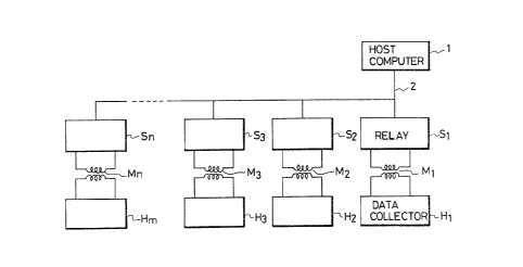
Referring now to the accompanying drawings, stationary data relays S1 to
Sn shown in Fig. 1 are placed between portable data collectors H1 to Hm and a
host computer 1, the communication is not performed directly between the
portable data collector H1 to Hm and the host computer 1 but is performed
relative to the data relays 50 as to be stored therein, and the data are sent
to the other unit from the data relays Sl to Sn. The communication between
the portable dsta collector H and the data relays is performed by
electromagnetic induction circuits M1 to Mn each employing a coil, in order to
eliminate connectors and to simplify the interface circuit. Thus, the
portable data collectors Hl to Hm are coupled to data relays Sl to Sn via
electromagnetic induction circuits M1 to Mn. When the portable data
collectors Hl to Hm are being carried, the data relays Sl to Sn are not
coupled to the portable data collectors ~ll to Hm, but wait to receive the
data. Further, the data relays Sl to Sn and the portable data collectors Hl
to Hn can be freely combined, and their numbers can be freely selected.
Fi8. 2 (dsscribed in more deta;l below) shows a method of couplin~ the
portable data collectors ~1 to Hm, to the data relays S1 to Sn. If the
portable data collector Hl is inserted and coupled into the data relay S1, the
PAT 10342-1
--3--
: . :
~:
~ ,
~;~8~
da~a ;al)ut ~o tdle poltable data collecto~ l~l a~e at once stored in the XAM ofthe data relay Sl. The host computer successively asks the data relays Sl to
Sn in rep,ard to whe~ller there i5 data vla a con~unication line 2. Only when
there is data, the data is transmitted and received between the host computer
1 and the data relay sl, and the data in the portable data collector Hl is
sent to the host computer 1. Durin~ this moment, the other data relays S2 to
s~ must wait for communications with the host computer 1. The communication
line 2 is formed by either wire or a radio link. The data relays Sl to Sn are
powered by an AC power supply or lar~e capacity DC power supply.
In the above-mentioned system, the data flow is as described below. That
is, when the data is to be transmitted from a portable data collector to the
host computer, both the data collector and the data relay have a coil so that
the data is transferred from the data collector to the data relay by
electroma~netic induction at a speed as low as 2400 bps, and is temporarily
stored in the RAM in the data relay and then the data is transferred from the
data relay to the central processin~ unit via a communication line at a speed
as hi~h as 9600 bps or more. In this case, it is also possible to change the
data format. When the data is to be transferred from the host computer to the
portable data collector, the flow of data is reversed. The interface between
the portable data collector and the data relay is formed by using a coil in
the casing without usine a connector. Therefore, the device exhibits
excellent moisture-proof property. Further, since there is no connector to be
attached or detached, the reliability is not deteriorated. Moreover, since
the transmission speed is as low as 2400 bps, the clock signal frequency can
be maintained small to consume reduced amounts of electric current. It is
further allowed to use a button-type lithium cell or a like cell, contributin~
to reducing the size and weight. Further, the communication is effected
between the host computer and the data relay at such a hi~h speed that it
solves the problem that a communication line is occupied by a portable data
collector which makes the communication, and the transmission or reception of
data from other portable data collectors must be waited for.
tationarY Data Relav
The stationary data relay allows for relaying data bi-directionally
between the host computer and portable data collector by settin~ the data
PAT 10342-1
--4--
~83~16
collector on a receivin~ surrace 102 shown in Fig. 2. The receiving surface
102 is inclirled by ahout 30 to 60 degrees so that the display unit 3 can be
easily s~en by an operator. An overhan~ 4 is provided at a portioll of the
data relay S to receive the portable data collector M in parallel with the
receiving sur~ace 102 which is provided with a recess having a curved surface
5 of a radius R with the edge P of the overhang as a center as shown in
Fig. 3. The curved surface S is made similar to a locus that is drawn when
the data collector M is turned with the edge P of the overhan~ as a center.
The data relay and the data collector have respective coils 7,6 responsive
to each other to provide communication therebetween when the data collector is
set on the data relay. Because the receiving surface is inclined, the coil 6
is brought into intimate contact with receiving surface 102, so that it is
placed in operative position relative to the coil 7.
According to this embodiment, the data collector can be attached and
detached favourably if the dimensional ratios (Fig. 3~ are selected to be
T:D:L:R ~ 5:6:5:8. Further, the bottom of the portable data collector M is
rounded as denoted by R, so that it can be handled comfortably. Fig. 4 is a
sectional view of an embodiment where the angle of inclination is 60 to 90
degrees. If the angle of inclination is close to 90 degrees, the portable
data collector M may fall forwardly. Therefore, a straight portion 8 is
provided under the curved s~rface 5, so that the portable data collector M is
prevented from falling forwards by means of the edge P o~ the overhang and the
straight portion 8.
As shown in Figs. 4 and 5 the portable data collector M can be inserted in
the receiving portion with an attitude I or II. When it is inserted with the
attitude I, a portion Q of the portable data collector M slides on the curved
surface 5 of the receiving portion, so that the attitude of the data collector
is changed from I to II. To take out the portable data collector M, it may be
tilted forward; i.e., the portable data collector turns with the edge P of the
overhang 4 as a center, and is removed without trouble. Further, the overhang
4 prevents the portable data collector M from escaping.
A circuit block diagram of the stationary data relay is shown in Fig. 6.
A CPU 9 controls a RAM 10 and and I/O interface 11 in accordance with a
program stored in a ROM 12. The data is transferred to and received from the
host computer 1 by a serial interface 13 relative to the central processing
PAT 10342-1
_5 _
~83~ L6
unit. The data ;s furtller transferred to and received from the portable data
collector by a s~riaL interface 14 relative to the portable data collector. A
printer drive circuit 15 executes hanushaking with the printer and produces a
print output. A circuit 16 ror driving the LED and bu~zer controls the LRD
and buzzer. A switch receiving circuit 17 informs the CPU 12 of the fact that
the switch is depressed.
If it is detected by the switch receiving circuit 17 that the portable
data collector is mounted on the data relay, the data is transferred to, and
received from, the portable data collector via the serial interface 14, and
the received data is temporarily stored in the RAM 10. Simultaneously with
the above-mentioned procedure or after the above-mentioned procedure has been
finished, the data is transferred to and received from the host computer via
the serial interface 13. The circuit 16 for driving the LE~ and bu~zer
indicates that the data is being transferred. Moreover, through the printer
drive circuit 15, messages from the portable data collector, from the central
processing uni.t, or from the data relay, are output to the printer. ~hen an
error has occurred during the above mentioned procedure, the circuit 16 for
driving the LED and buzzer informs the user of the occurrence of the error.
If the host computer transfers the same data to a plurality of portable data
collectors, the data relay perpetually stores the data sent from the host
computer into RAM and then the data relay transfers the stored data to a
plurality of portable data collectors. A circuit diagram of the serial
interface 14 relative to the portable data collector is shown in Fig. 7. A
transmitting terminal 18 is provided for inputting a signal from the CPU. The
signal represents the data to be transmitted to the portable data collector
and is connected to a transmitting unit 19 which consists of resistors 20 and
21, a transmitting transistor 22 and diode 23. The anode terminal of the
diode 23 is connected, via a contact point 24, to a tuning unit 25 which
consists of a transmitting/receiving antenna coil 7 and a tuning capacitor 27
which are connected in parallel with each other.
A receiving circuit 28 comprises a coupling capacitor 29, resistors 30 and
31, a clipping diode 32, a receiving transistor 33, and a resistor 34 and
includes a high-pass filter which consists of the capacitor 29 and the
resistors 30, 31 and which is connected, via the contact point 24, to the
transmitting unit 19 and to the tuning unit 25. The receiving terminal 35 is
PAT 10342-1
--6--
:
~f33~,16
connec~ed to the colLeclor of the receivin~ transistor 33.
The si~nal input to the tlansmitting te~inal ]8 is sent to the base
terminal of t.he transmitt;ng ~ransistor 22 via a transistor drive unit which
consists of the resistors 20 and 21, and causes the transmittin~ transistor 22
to be switched. When the transmitting transistor 22 is rendered conductive,
the contact point 24 assumes ground potential. When the transmitting
transistor 22 is ren~ered nonconductive, the contact point 24 assumes a high
level to excite the transmittin~/receiving antenna coil 7. Under this
condition, the signal is transmitted to the base of the receiving transistor
33 via coupling capacitor 29, resistor 30, clipping diode 32 and resistor 31,
to render the receiving transistor 33 off or on. Consequently, a signal
appears on the receiving terminal 35 having a phase opposite to that of the
signal input to the transmitting terminal 18. Here, if the terminal 24 is
poorly connected or if the transmitting/receiving antenna coil 7 is broken,
the receiving transistor 33 remains nonconductive irrespective of whether the
transmitting transistor 22 is rendered conductive or nonconductive, and the
signal being transmitted does not appear on the receiving terminal 35.
On the other hand, if an excessive signal is inputted to the transmitting
terminal 18 or if supply noise is generated, diode 23 prevent a current
flowing from base to collector of transistor 22.
The serial interface 13 relative to the central processing unit may employ
the same circuit as that of the serial interface 14 above described. Also the
serial interface may employ an ~IA standardized interface, for example as 422
or RS 232C as a high speed interface.
Portable Data Collector
The portable data collector M for collecting the data and for transfering
the data to the stationa~y data relay has the display unit 3 located on the
upper portion of the case 37 as shown in Fig. 8. The portable data collector
also has input keys 38. These input keys 38 are arranged on both inner sides
of the case 37, which is able to open as shown in Fig. 8. When a user inputs
data, the user opens the case 37 and depresses the keys 38.
Fig. 9 is a sectional view of an input key, wherein a menu paper 39
describing menus is placed on a membrane switch 40 and the surface of the menu
paper is protected by a protecting sheet 41. The menu paper 39 consists of a
paper produced from a printer and describes menus that are printed thereon.
PAT 10342-1
~ -7-
321~
~he pro~ctin~ sh~et 41 has lines to meet thc keys o~ the membrane switches
40. ~ach ke~ has four m~nus and any one of them is selected by depressin~ a
select key (not sho~) in advance.
Fig. 10 is a functional diagram of the portable data collector.
The portable data collector registers processes received from an external
unit and addresses of processes corresponding to all of the keys in the RAM.
The addresses are changed by an external unit, so that the ~unctions of
given keys can be changed.
A key input means 42 is connected to a process select execution means 43.
A key process correspondence memory 44 and a process msmory 45 are also
connected to the process select execution means 43. The process memory 45
consists of an initial registration process memory 46 and an additional
registration process memory 47. The key process correspondence memory 44 and
the additionsl registration process memory 47 are connected to a received data
registration changing means 48 which receives signals sent from an external
key process registration means 49.
If a key si~nal is input from the key input means 42, the process select
execution means 43 selects a process that corresponds to the key signal from
the key process correspondence means 44. The content of the selected process
is registered in the initial registration process memory 46 or in the
additional registration process memory 47 in the process memory 45 and the
process select execution means 43 looks in the process memory 45 for a process
that is selected from the key process correspondence memory 44 and executes
the process. Under the initial condition, there is no ~ontent in the
additional registration process memory 47. The additional registration
process memory 47 is used for the first time when a process is registered
therein by the external key process registration means 49 via the received
data registration changing means 48. In response to signals from the external
key process registration means 49, the received data registration changing
means 48 reeisters the process into the additional registration process memory
47 and changes the content of the key process correspondence memory 44. The
key process correspondence memory 44 stores the correspondence of processes
relative to the keys. By registering a new process in the additional
registration process memory 47 from the external key process re~istration
changing means 49 in order to change the process of the key process
PAT 10342-1
--8--
3~6
corcespotldence mem~ry 44 relative to the keys, it is possibLe to change the
func~ion of any key.
~ ig. 11 is a flow chart showing the flow of operation of the pl'OCeSS
select execution means 43, and Fi~. 12 is a flow chart of the operation for
chatlging the key functions. The invention will now be explained in
conjunction with these flow charts. In Fig. 11, a key Ki is depressed at a
step (1). The process select execution means 43 selects from the key process
correspondence memory 44 the address of a process that corresponds to the key
Ki at a step (2). The process select execution means 43 looks in the process
memory 45 for a process represented by the address of the selected process at
a step (3), and executes the process at a step (4). By changing the address
of the process corresponding to the key in the key process correspondence
memory 44, therefore, the key function can be changed. When a new function
that has not been registered in the process memory 45 is to be accorded that
key, the process should be newly registered from the external key process
registration means 4g via the received data registration changing means 48.
In Fig. 12, a new process is re~istered in the additional registration process
memory 47 from the external key process changing means 49 via the received
data registration changing means 48 at a step (5). ~ext, at a step (6), a key
portion to change the function of the key process correspondence memory 44 is
changed into the address of a newly registered process by the external Xey
process changing means 49 via the received data registration changing means 48.
How the key functions are changed will now be described by way of a
concrete example of Figs. 13 to 17. Fig. 13 is a diagram of the portable data
collector having 20 keys Kl to K20. Fig. lb is a diagram in which functions
Fl to F20 are allotted to the keys Kl to K20. That is, Fig. 14 describes the
functions of the keys in such a manner that a process Fl is performed if the
key Kl is depressed, and a process F2 is performed if the key K2 is
depressed. Fig. 15 shows the contents of the key process correspondence
memory 44 that satisfy the key functions of Fig. 14. The address of the
process Fl enters into a portion in which is stored the address of a process
that will be executed when the key Kl is depressed. Similarly, the address of
the process F2 enters into a portion that corresponds to the key K2. Further,
the addresses of processes Fl to F20 are entered to correspond to the keys K1
to K20. The processes F1 to F20 are registered in the initial registration
PAT 10342-1
3Z~6
pro~ss memory 4~ in the proc~ss memory 45, but are not re~ister~d in the
additional registration process memory 47. In practice, any processes may be
referred to as the processes Fl to F20; e.g., the key that is rc~istered at
first may bc proc~ssed. If now the key Kl is depressed, this fact is informed
from the key input means 42 to the process select execution means 43. The
process select execution means 43 selects, from the key process correspondence
memory 44, the address of a process which corresponds to the key Kl. Here,
since the contents of the key process correspondence memory 44 are as shown in
Fi~. 15, the process Fl is selected and is executed. The practical contents
of the process Fl are stored in the initial registration process memory in the
process memory 4S. By forming the key process correspondence memory 44 as
shown in Fig. 15, the key functions can be arran~ed as shown in Fig. 14.
Wext, with reference to FiB. 16, the processes F5 to F20 are effected in the
same manner as described above without chan~in~ the functions of the keys KS
to K20, but changing the processes Fl to F4 of the existin~ functions of the
keys K1 to K4 into the processes F20 to F24 that have not been re~istered in
the process memory 45. The processes F20 to F24 are newly re~istered in the
additional registration process memory 47 in the process memory 45 by the
external key process re~istration means 49 via the received data registration
chan~ing means 48. The contents of the key process correspondence memory 44
are then chan~ed as shown in Fig. 17 by the external key process re~istration
means 49 via the received data registration changing means 48. Namely, the
address of process F21 is entered into a portion in which is entered the
address of the process of key Kl, and similarly, F22 is entered into K2, F23
is entered into K3, and F24 is entered into K4. Therefore, if the key ~l is
depressed, the process select execution means selects the process F21 that
corresponds to the key Kl in the key process correspondence memory 44 of Fig.
17, and executes the process that is stored in the additionsl ro~istration
process memory 47. The key functions are thus arranged as shown in Fi~. 16.
As described above, new functions can be imparted to ~iven Xeys by registered
processes from an external unit into the additional registration process
memory 47 and by chan~ing the contents in the key process correspondence
memory 44.
Fig. 18 is a circuit block diagram of the portable data collector which
reali~es the functions mentioned above. Two hi~h-performance lithium
PAT 10342-1
--10--
.,
: ' ' '
' : :
:
16
ba~teties are connected in series to {orm a cell 50, and a constant volt~ge of
three volts is ob~aine~ through a power supply circuit 51. The consumption of
electric current increascs with the increase in the power supply voltage As
the power supply voltage decreases, on the other hand, the operation frequency
of each IC decreases and the system becomes defective. A voltage of three
volts is suitable for this system. A cell voltage detecting circuit 52
functions to detect the drop in the cell voltage, and details of this circuit
will be described hereinafter. A ROM 53 stores an initial program which is
necessary for starting the system and a subroutine that is frequently used.
The practical procedure for collecting data and the items of the input keys
are all written into RAM 54 from the data relay by electromagnetic induction
through a transmittin~/receiving coil 6 and an interface LSI that controls the
coil 6. The CPU 55 and the interface LSI 56 have an oscillating circuit,
respectively, and generate clock signals necessary for the driving. The CPU
55 oscillates at about 1 ~Hz and starts to oscillate only when an interrupt
signal is received from the interface LSI 56 in response to key input or
transfer of data, and ceases to oscillate after a predetermined process has
been finished. The interface LSI 56, on the other hand, oscillates at all
times. A cheaply constructed tuning fork-type quartz oscillator which
oscillates at 38.4 KHz can be used. A tuning fork-type quartz oscillator for
timekeeping devices which oscillates at 32768 Hz is cheaper since it is widely
used. However, a quartz oscillator which oscillates at 38.4 KHz is used when
it is required to set the transfer speed relative to the external unit to be
an integral multiple of a standard value of 1200 bps. Thus, the oscillating
circuit is divided into two, and the one on the CPU 55 side is not operated
except for a required moment, so that the average consumption of current is
greatly reduced. The interface LSI 56 further has a communications control
function necessary for the data communication, a function for controlling the
input keys 38, a function for generating an operation confirmation sound
signal, and a function for controlling a variety of CPU's 55 and the display
unit 57. The volume of operation confirmation sound can be increased or
decreased. A circuit for coupling to the data relay may employ the same
circuit shown in Fig. 7.
A display unit 57 consists of a common signal generating cicuit 57a, a
segment signal generating circuit 57b, and a multi-character-dot-matrix liquid
PAT 10342-1
crystal liisp~i~y )~(m The ]iquid crysta~ display must be driven by AC signals
to prcvcnt i~ fl~om ~telioratillg, and its contrast is adjusted by changing the
ampLitude of th~ AC signals. The portable data collector which has collected
the data ~hen trans~ers the data to an external unit. At this moment, signals
are transfel~r~d ~Lom the interface LSI 56 to the data relay device via the
transmitting~receiving coil 6. After the data has been transferred, the
contrast is decreased to decrease the consumption of electric current by the
multi-charact~r--dot-matrix liquid crystal display 57c.
Fig. 19 is a dia~ram which illustrates in detail the cell voltage
detecting circuit 52 of Fig. 18. When the CPU 55 is not in operation, an HLT
si~nal assumes the "L" level, whereby a transistor 58 is rendered
nonconductive to interrupt the supply of power to a voltage detecting element
59, to thereby decrease the consumption of electric current. When the power
source voltage is greater than about 3.3 volts, the voltage detecting element
59 directly produces the power supply voltage. Since a new cell produce a
voltage of as great as 6 volts, the voltage detecting element cannot be
directly connected to the CPU 55. Therefore, the level is changed through a
transistor 60. When the cell volta~e is normal, furthermore, the transistor
60 is rendered nonconductive so that no electric current is consumed. When
the cell voltage drops to lower than 3.3 volts, the element is not destroyed
since the difference is small relative to the power source voltage of an
inverter 61 of the next stage. The output of the inverter 61 passes through a
CMOS analog switch 62, and is read as an I0 output into the data of the CPU 55.
The display unit 57 will now be described in detail with reference to
Fig. 20. The common signal generlting circuit 57a contains a display RAM and
a character ROM (which are not shown), and is connected to the CPU 55 through
an address bus, a data bus and other signal lines. As a signal is sent in the
form of ASC II codes or the like from the CPU 55, the common signal generating
circuit 57a converts it into character pattern data, latches it, sends the
data to the segment signal generating circuit 57b, and generates a common
signal which will be sent to the multi-character-dot-matrix liquid crystal
display 57c. In response to the character pattern data from the common signal
generating circuit 57a, the segment signal generating circuit 57b generates
segment signals that correspond to dots of the multi-character-dot-matrix
liquid crystal display 57c. The contrast is changed by changing the peak
PAT 1034~
-12-
.
:
~33~6
values of co~ on si~nals and segmellt si~nals by using a booster circuit in the
common siglla~ geTlcratillg circu;t 57a.
Fig. 21 is a dia~ram illustrating a part of the common signal Keneratin~
CiL'CUit 57a. ~ ga~e control circuit 63 operates depending upon the contrast
data sent over the address bus and the data bus. A dividing resistor 64 is
driven on a constant cur~ent, and a potential at a given connèction point is
taken out by an analo~ switch 65 controlled by the gate control circuit 63 and
by a voltage follower 66.
Fi~. 22 shows common signals and se~ment si~nals. The common signals have
peak values of four levels and the segment signals have peaX values of three
levels. The display element does not turn on when the difference between the
signals is one level but turns on when the difference between thè signals is
four levels.
The liquid crystal display element can generally be regarded as a
capacitor which, when an AC voltage is applied thereto, permits a current to
flow through it depending upon the amplitude and the frequency. An AC voltage
of a certain value is normally applied also to those segments that are not
turned on, so that a current flows through them even when the polarity of the
signal is changed. The current that is consumed while the CPU 55 is not in
operation consists of a current that flows through the interface LSI 56 and
the display unit 57, and a current that flows through the li~uid crystal
display elements. The multi-character-dot-matrix liquid crystal display 57c
is considered to be composed of a large number of capacitors, and consumes a
large current to produce the display. Considered below is the case where the
contrast is decreased. As the output of the booster circuit decreases, peak
values of the common signals and the segment signals decrease, whereby the
amplitude of the AC voltage applied to the liquid crystal display elements
decreases and the current flowing through them decreases. This is the
condition where the contrast is decreased. Here, attention should be given to
the fact that a DC voltage should not be applied to the liquid crystal display
elements to prevent them from deteriorating.
The CPU 55 operates for a very short period of time, and an average
current is considerably smaller than that which flows into the CPU 55 when it
is not in operation. Therefore, to decrease the current that is consumed when
the CPU 55 is not in operation serves as a key to the cell system.
PAT 10342-1
-13-
The cell life will l)e calculated below based upon practical examples.
(1) It is presumed that the data is itlp~lt and is trans~erred, requirirlg a
time o~ one hour.
(2) The CPU consumes a current of 1.2 mA when it is in operation. In the
portable dat~ collector ~hich consumes a small current, however, the CPU is
usually not in operation.
(3~ When the CPU is not in operation, the current being consumed is 40 ~A
when the contrast is the greatést and is 20 uA when the contrast is the
smallest.
(4) If the CPU operates for 100 seconds a day, the average current that is
consumed is calculated as follows:
in the case of non-chan~ing the contrast
100 sec. x 1.2 mA/86400 sec. + 40 uA = 41.39 uA
in the case of changing the contrast
100 sec. x 1.2 mA/86400 sec. + (20x24+40x2-4)uA = 23.61 uA
(S) When a cell having a capacity of 120 mAh is used, the serviceable life is
calculated as follows:
in the case of non-changing the contrast
120 x 10
4l.39 x lO . 24 . 121 days
in the case of changing the contrast
120 x 10
23.61 x lO 6 . 24 .- 212 days
PAT 10342-1