Note: Descriptions are shown in the official language in which they were submitted.
3~
20161 -1-
APPARAI'US AND METHOD FOR REGISTRATION OF
SHADOW MASKED THIN-FILM PATTERNS
CROSS-REFERENCE TO CO-PENDING APPLICATIONS
In co-pending Canadian patent application Serial No.
519,973-5 ("Mask for Patterning Electrode Structures in
Thin-Film EL Devices", Robert Boudreau), there is defined a
mask structure and a method of fabricating electrode
structures for a thin~film EL device that utilizes such a mask
structure.
In co-pending Canadian patent application Serial No.
519,972-7 ("Mask Assembly Having Mask Stress Relieving
Feature", Robert Boudreau), there is defined a mask assembly
that provides support for a shadow mask while eliminating mask
wrinkling during patterning of thin-film structures.
Both of the above applications are filed concurrently
herewith and are assigned to the same assignee as the instant
invention.
TECHNICAL FIELD
The present invention relates in general to the deposition
of depositing thin-film structures, and particularly to an
apparatus and a method for thin-film structure patterns on a
substrate for a thin-film display device.
~'~
l~.'
, '` ' ' '
.
,
!
B5-1-095 -2- PATENT
BACKG~OUND OF THE INV~NTION
Thin-fil~ di play panel6 (6uch a6 LCD or
electroluminescent) hav~ been known to be very useful for
di6playing information a6 the thin-film fitructure6
incluaing the cro~ electrode~ and contact pad6, can be
depositea on a gla66 ~ub~trate thereby providing a matrix
di6play panel capable of being ~electively energized to
activate indivi~ual pixel~ thereon. One o~ t~e problem6
encountere~ in the manufacture of thin ~ilm di6play panels
i~ the development of proce~e~ that pattern the thin ~ilm
electrode ~tructures while in an in-line depo6ition 6y6~em.
Most thin-film ~evice6 have had their thin-film
structure6 patterned either by a ~e~ process ~nown a6
photolithogr~phy or by ~hadow ma6kin~. Photolithography
15 i6 very similar to proce~e~ u~ed to develop photograph~
in that the ~epo~it to be patterned i6 coated with
light-6e~sitive material. which i~ then expo6ed-to a~
negative or po6itive pattern and then developed and later
strieped in various corro~ive developinq 601ution~. The
di6advantage~ of this method i~ t~at it i~ 810w and labor
inten6ive. and involves many step~, each one ~ub3ect to
failure or po~sible contamination of the thin-film device.
~ ith re~pect to the u6e of 6hadow ~a6king to depo6it
thin-fil~ 6tructures, reference i~ made to U.S. Patent
2~ 4,335,161 to Fang C. Luo, entitled "Thin-Film Tran6istors,
Thin-Fil~ Transistor Array~ and a Process for Preparing
the 5ame". In ~ummary. the Luo patent appears to di~clo6e
a met~od of preparing a th;n-film ~ran6istor or an array
of thin-fil~ tran6i6tor6 by depo6iting in vacuum the
different c~mponents through a 6ingle apertured
,
.
85-1-095 -3- PATEN~
~ask,wherein the ~pertured ma~k i8 ~ovea in predetermined
pattern ~or the ~epo6ition of each of the component6. In
Luo. once the depo~ition of the dif~erent structure6 is
complete. the ~6embly that is formed i~ then removed from
the vacuum and the fabrication completed by te~hniques
suc~ as p~otolithograp~y.
As in Luo. shadow ma~king i~ u~ually performed over
small sub~trate6 with stiff mask6 that are manually
clamped to en~ure even contact with a particular
substrate. This is a relatively 610w proce~s and u~ually
reguire~ breaking vacuum in the depo ition cham~er,
re~ultinq in some thin-film contamination. When
depositing throug~ a large area ma~. it i~ common that
the ~ub~trate i~ not perfectly flat or not level with
re~pect to its ~urrounding fiubstrate holder. The pre~ent
inve~tion addres~es the problem ari~ing from the
difficultie~ of remote automatic handling of large area
~hado~ ~sks in an in-line deposition sy6tem. -
~ ith re6pect to the use o~ photolithography, thin-film
patterns have typically been aligned to the substrate and
20 each other by optical means and the su~trate i6 moved
mannally into position with t~e aid of a micromanipulator
or an op~ical ~canner which provides information to a
co~puter which performs a 6imilar function. The aligned
sub~trate i~ then expo~ed and wet processed ~o achieve the
de~irea pattern. In contra~t, most shadow ~a6king
i proce~ses are aligned manually by dropping the maskL over
pin~ located on a ~ubstrate carrier. There~ore. an
apparatus which i~ effective for remotely operating
auto~aeic ma~ki~g ~yseem~ ~here there is a need to
eli~inate the need for ~reaking vacuum, which would
conta~inate depo6it of thin film6, would be con~idered an
advancement in the art.
: . .
3~
85-1-095 -~- PAT~NT
DISCL05URE OP THE INVENTION
It i~ therefore a primary object of thi6 invention to
enhance t~e art of thin-film 6tructure depo~it~on. and
particularly the art invol~ing thin-film display panels.
It i~ another object of this invention to provide an
apparatu~ for aiding in the alignment of thin-film
structures patterne~ in thin-film device6.
seill ano~her object of the inven~ion ifi to provide a
method of ~ligning thin-film ~truc~ure~ that are to be
patterned on the ~ub~trate through the u6e of a vacuum
deposition proce~s.
A further object of the present invention is to
provi~e an apparatu~ and a method for automatically
aligning thin-film ~tructure~ to be patterned on a
6ub6trate while in an ;n-li~e depo6ition ~y~tem.
I~ aocoraance with one a~pect of thi~ invention. there
i8 proyi~ea an apparatu~ for the alignme~t of thin-film
~tru~ture p~ttern~ on a substrate formed with the use of
an aperturea ~as~ in a vacuum deposition sy~tem. ~he
20 apparatu~ compri~e~ a mask frame and a ~a~k assembly
~ffixed to the ma~k frame, the ~ask a6~embly including the
aperturea mal;k and ma~k alignment apertures which are
~î~po~ea on either ~ide of the ma k. A ma~k holder frame
is positioned adjacent the mas~ assembly and is affi~ed to
the ~a~ frame to form a mask holder as~embly, the mas~
holder a~sembly having pri~ary datum pin~ affixed thereto
¦ and protruding from the side of the ~older as~embly
oppo~ite ~aid ma~k as6embly. Finally. the aliqnment
apparatu6 inclu~e~ a ~ub~trate carrier, having a ~ub6trate
85-l-Q95 -5- PATEN~
6upporte~ therein, po~iti~nea aa3acent and in operati~e
contact with ~a~k hol~er a6sembly; the sub~trate carrier
has primary ~atum ~perture6, that engage wi~ the pr~ary
pins of ehe ma6k holder as~embly. w~ich are di~po~ed on
the periphery of the carrier. In addition, the carrier
has ~econ~ary aatum pin~ protrudinq therefrom that engage
with ~he mas~ alignment aperture6 of the mask as6embly.
I~ accordance with another a~pect of thi~ invention,
there i~ provi~ed a me~hod of aligning thin-film structure
pattern~ on a ~ubstrate for~ed with the u6e of an
10 ~pertured ma~k in a vacuum depo~ition ~y6tem. The
alignment ~ethod compri~es the ~tep~ of positioning a mask
hol~er a6~embly within a depo~ition chamber, ~uch holder
a~sembly having the apertured ma~k a~ par~ thereof and
h~ving means for engaging a 6ubstrate carrier. A
sub~trate carrier i~ then po~itioned ~i~hin the depo~ition
chamber spaced fro~ the ma~k holder as~embly, the carrier ~
having the ~ub~trate suppor~ed-therein and having ~eans
for aligning the apertured ma~k with the sub~trate. The
ma~k ~ol~er as~embly i~ then engaged wit~ the sub~trate
carrier 6uch tha~ they are i~ operative contact. A magnet
is then po~itioned in the dep~6ition chamber adjacent the
side of the r~ub~trate carrier oppo~ite the ma~k holder
afi~e~bly ~uch that the apertured ~a~k i~ held in operative
contact with ~he substrate. ~urthermore. a thin-~ilm
structure material is then vacuum-depo~ited through the
~p0rtured ~a~k ~n~ the ~agnet i8 t~en remoYed from the
; sub~trate carrier and the mas~ holder a~e~bly di6engaged
from the sub~trate carrier. thereby re~ulting in the
for~ation of thin-film ~tructure~ ~n the ~ubstrate.
85-1-095 -6- PATENT
In acc~r~ance w~th still another a6pect of th~6
invention, there i~ provided a method of aligning
thin-film 6tructure pattern~ on a 6ub6trate formed with
the use of an apertured mask in a vacuu~ depo~ition
~y6te~. T~e alignment me~hod co~prises the 6tep6 of
providing a mask frame and affixing a ma6k a66embly to the
ma6~ frame. the ma~k a66embly including the apertured ma~k
an~ ~a~k alignment apertures that ~re di~po6ed on either
8iae of the ma6~. A ma~k holder frame is affixed through
the ~ask a~embly to the ma~k frame to form a mask holder
a~se~bly. the ma~k holder a~embly having primary datum
pins affixed t~erethrough and protruding from the ~ide
oppo6ite the ma~k assembly. The ma6k holder a6~embly i~
then po6itioned in ~ vacuum depo~ition chamber while a
sub~trate carrier i6 then po~itioned in the depo~ition
chamber fipaced from the ~a6~ holaer a~sembly. The carrier
ha~ the su~6trate supported ~herein and ha~ primary~datum
~pertures ~ispo~ed about- the-periphery of the carrier; the
carrier ha~ ~econdary datum pins protruding from the 6ide
ad3acent the mafik holder assembly. The ma~ holder
~s~e~bly i~ then engaged ~ith the 6ubstrate carrier 6UCh
that the primary datum pin~ are f ir8t engaged with the
pri~ary apertures of the ~arrier while the 6econdary datum
pin~ are 6ubsequently engaged with the ~a6k alignment
aperture~ of the ma6~ a~sembly. Next, a magnet i~
po~itioned i~ the depo~ition cha~ber adjacent the ~ide of
the carrier opposite the ~a~ holder a6sembly such that
t~e aperture~ ma~ held in operative contact with the
sub~trate; a thin-film ~tructure material i~ then
vacu~-depo~itea through the apertured ~a6~. Finally, the
mag~et i~ remo~ed from the ~ub6trate carrier and the ma6~
8 5 ~1- O 9 5 - 7 - PATENT
holder as6embly is di6engaged ~rom the su~Rtrate carrier
~here~y re6ul~in~ in the formation of thin-film 6tructures
on t~e 6ubstrate.
BRIEF DESCRIPTION OP TH~ DRA~INGS
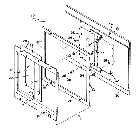
~IG. 1 illu~trates an example of an embodiment of the
apparatu~ for aligning an apertured ~a~k again~t a
substrate, and
~IGr 2 illu~trate~ an example of the alignment
a~paratu~ of FIG. 1 within a deposition chamber that
aid~ in ~escribing the automati~ aligning procedure.
B~ST ~ODE ~OR CARRYING OUT THE INVENTION
Por a better under~tanding of the pre6ent invention,
tog~t~er with other and further objects, advantages and
capa~;lities thereof, reference is made to the following
disclo~ure and appended claims in connection ~ith the
above-~e~cribed ~rawings.
~ith p~rticular attention to PIG. 1, there i~
illu~tr~ted a mask alignment or regiGtration apparatus for
ultima~ely ~ligning an apertured mask to a glass substrate
on ~ich thiu-film structure~ are to be deposited.
Align~ent apparatus 10 i8 primarily compri~ed of a ~as~
hol~er 12 ~nd a sub~trate carrier 30, ~hich supports (in
this ~ase) t~o ~ub~trates. In particular, mask holder
a~e~bly 12 i6 comprised of a mask frame 14, a ~ask
a6~2~1y 20 and a mask holder frame 26. In this
particular embodiment mas~ frame 14 is ~ub6tantially
3~ ~1
~5-1-095 -9- PAT~NT
rectan~ul~r in shape and ha6 a frame ce~ter ~upport 16,
which support6 one 6et of 6pring for~ 18 that aid in
engagi~g ma~k assembly 20 with ~ub6trate carrier 30, and
~as ~a~ frame pin6 17 (~ee PIG. l~. ~as~ holder frame 26
al~o ~a~ pin6 27 located about its periphery (e.g. top and
~otto~) for allowing ~ask frame 14 to be affixed thereon.
Ma~ a6~embly 20 ha6 ~ounting hole~ 21. for mounting
ma~ a~embly 20 to mask ~rame pin~ 17, a~d 6upports an
apertured ma~ 22 which aid~ in depo~iting thin-~ilm
~tructure~ on a gl~8 6ub6trate. ~ask a~sembly 29 al~o
has ~a~k alignment aperture~ 24 disposed on either 6ide of
~pertured mask 22. In addition, mas~ holder frame 26 ha6
primary datum pin6 28 affixed thereto and protruding from
the side opposite mas~ a~sembly 20. A~ will be de~cribed
in ~etail later in the Specification, primary datum pins
28 ~ærve to engage mas~ holder a~sembly 12 with sub~trate
carrier 30.
~ eferri~g again to FIG. l. In thi~ particular
embodiment substrate carri~r 30 i6 illustrated having at
least two ~ub~trate~ 32 ~upported therein. Substrate
carrier 30 is al~o sub~tantially rectangular i~ shape and
ha~ primary aperture~ 34 di~po~ed about it6 periphery for
eng~ging the primary ~atu~ pin~ 28 of mask holder as~embly
12. Primary aperture6 34 in this ca6e are two in number
~nd are typically named alignment or registration holes
for the purpose of aligning ma~ holder as6embly 12,
~ co~taining mas~ a~6embly 20 with 6ub6trates 32 of
I ~ubstrate carrier 30. The present inventio~ operate~ on
the ba6is of a primary and ~eco~dary datum referen~e
location~. The pri~ary datum reference locatum i8
achieved when substrate carrier 30 i~ positioned adjacent
and i~ operative contact with ma~ holder as~embly 12 ~uch
B5-1-095 -9- PAT~NT
t~t pri~ary ~tum aperture~ 34 will engage with pri~ary
datun pins 28. Sub~trate carrier 30 al~o ha6 a serie~ of
6econdary datu~ pins 36 protruding therefrom that are
diEpo~ed on ehe ~arrier side faci~g ma6k holder assembly
lZ. Secondary datum pin6 36 will ultimately engage with
6econdary ~a~k ~lignment aperture~ 24 of mask a6sembly
20. T~i~ engagement will nudge apertured ~ask 22 into the
higher accur~cy secon~ry datum reference location (i.e.
pin~ 36 and aperture6 2~) in order to properly align
~pe~turea mask 22 with on0 of the sub6~rates 32.
~pring forks 18 of mask frame 14 are considered mean~
for aiding the engagement of ma6k asse~bly 20 with
secondary datum pins 36 of substrate carrier 30. The
spring fork~ are located sub6tantially within and coplanar
wit~ ~a~ frame 14. A spring fork (i.e. 18) is included
for eac~ of the secondary datum (i.e. 36) pin~ and are in
operative contact with mask afisemb-ly 20 while being
aligned wit~ m~s~ ~lignment aperture6 24. In addition.
apertured mask 22 is structurally relieved from mask
asse~bly 20, which i8 rigidly attached within mask holder
asse~bly 12. such that ~he mask i~ capable of being in
operatiYe contact wit~ the sub6trate of sub6tlate carrier
30. ~k al;gn~ent aperture~ 24 of ma~k a~sembly 20
incluae a ho:Le and slot that engage with secondary pin~ 36
of ~ub~trate carrier 30, a~ illustrated in FIG. 1, and
~o~plete the ~econaary datum reference. As will be
de~ribea in further ~etail in FIG. 2 and later in the
Specification, alignment apparatus 10 further include6 a
mag~et 56 disposed adjacent and i~ operative contac~ ~ith
6ub~trate carrier 30. ~agnet 56 is disposed on the side
3~ of carrier 30 opposite ~as~ holder frame 26. Apertured
85-1-095 -10- PATENT
ma~ 22, i~ thi~ p~rtisular e~bod~ment, can be decigned
for patterning electrode ctructures or ele~trDde pad
contact6. but ic not limited to cuch ~tructures.
T~e apparatuc de~cribed in this invention i~ moct
effective for remotely operated automatic mac~ing 8y6tem~
where there i~ a need to eliminate ~he breaking of vacuum
which c~n eontaminate the depocited thin-film6. The
invention provi~e~ ~ final secondary "chort cut" datum
regictration or alignment cy~te~ eliminating tolerance
build-up caused by chained interregi~tration of many
separate p~rtc by leaping over the~e regictrations and
creating a new, in~ependent datum. Without the final
6econdary "~hort cut" datum regi~tration afforded by thi~
invention, regictration would be through a seriec of datum
ma~k holder pin~, carrier bu~hingc, tooling and glacs
holder~ ~ven ~ith a 0.001 in~h tolerance for each
ma~hined part. the t~tal tolerance would be greater than
0.005 inch an~ unacceptable toward making the pattern~
regicter for electrical connection off of a glacc display
~ub6trate. Furt~ermore, the method for providing the
final regictration muct be compatible with mechanical
chadow ma~king to prevent blurc and defectL in the
resulting patterns.
~ e have diccovered that our pre~ent ma~ decign allows
enough forced movement of apertured mack 22 about its
prirary datum reference location through a crude ceriec of
chai~e~ aatums, that ~ cecondary independ0nt datum can be
uced to make a more precice final regi~tration of
apertured mack 22. The cecondary independent da~umJ in
; this ~e cecondary datum pins 36 ~nd mack alignment
aper~ture~ 2~. bringc t~e pattern regiceration within the
difficul~ tolerance needed to make a ~hin-film ctructure
85-1-095 ~ PATENT
for a thin-film ~evice~ In FIG. 1 the locati~n of ~he
large pri~ary ~hained datu~ regifitration pins 28 register
~a~k assembly 12 to substrate carrier 30. The lo~ation of
the ~u~h ~maller secondary datu~ pins help register
aperturea ma6k Z2 to 6ub~trate 32 with high precision.
This invention requires the less accurate chained
registratio~ sy~em li.e.. primary datum pin6 28 and
primary ~pertures 3q) to get tolerances within a certain
range to allow the secondary datu~ system of the invention
So engage and take effect.
A typieal operation of the alignment apparatus'
primary and secondary datum referenee sy6tem consi6t6 of
ulti~aeely locating ma~k assembly 20 over secondary datum
pin6 36. by fir~t engaging mask holder assembly 12 with
the less accurate, chained primary datum o~ mask frame 14
and ~ubstrate carrier 30. As mask holder assembly 12
reaches the end of its~primary engagement stro~e, mask
- - a~se~bly ~0 begins to pu~h ~ask alignment apertures 2~
over the ~horter length ~econdary datum pins 36. Thi6
engd~ement nudges the apertured mask 22 into the higher
ac~uracy secondary datum reference location. Spring forks
18, ~ounted on and about ma~k frame 14. aid in the
eng~gement o~ alignment apertures 24 with secondary pin~
36. The spring forks pre6~ on ~ask as6embly 20 only at
the ~e~ondary pin location~ 60 t~at friction does not
25 inhibit lateral movement of mask assembly 20 which would
prevent it from aligning with ehe pin position. ~lso,
pressing at only the pin locations reduces mask stre
which ~an blur the ~a~ pattern during the subEequent
dep~sition step. After mask as6embly 2Q is neatly e~gaged
on ~econdary pins 36, a hold-down system such as magnet 56
brings ~ask 22 tight again~t qlass substrate 32.
85-1 095 -12- PATENT
Seco~dary regiçtra~ion or ~lignment i6 be6t perfor~ed by
using ~pecially ~hape~ aperture~ 24: a hole on one side of
ma~k 22 and a ~lot on the other ~ide so tha~ secondary
pin~ 36, utiliz~ng the~e holes, do not bind with each
other. Binding of the secondary datu~6 w;th the primary
datu~s does noe occur becau~e the alignment error between
the 6eparate datums is le66 than the flexible movement of
ma~ 22.
aeferring now to PIG. 2. ~here is illustrated
aligument apparatu~ 10 inside a vacuum deposition cha~ber
50 alo~g witA magnet 56 and sputtering apparatu~ 52. FI~.
2 illustrate~ a portion of a depo~ition &ystem which may
either be from an in-line or from a batch process type
~y6te~. Sputtering apparatus 52 also has a layer of
depocition material 54 ~hereon which will be depo6ited
15 thr~ugh apertured ma~k 22 snto one of the fiub6trates of
substrate carrier 30.
- T~e following will be a de~cript;on of the method of
ing thin-film ~truc~ure patter~ on a substrate
for~ea with the use of an apertured ~ask in a vacuum
deposition sy~tem. With the aid of ~IG. 2. t~e ~ethod
comprise6 the steps of po~itioning a ~as~ hold~r assembly
12 ~nthin a ~po~ition shamber 50, mas~ holder a6sembly 12
having ~pertured mas~ 22 as part thereof and having means
for eng~ging substrate carrier 30. A sub~trate carrier 30
is t~en po~itio~ed within depo~ition chamber 50 spaced
LO~ aas~ holder assembly 12. carrier 30 having a
sub~trate supported therein and having mean~ for aligning
apertured masl~ 22 with the ~ub~trate. Ne~ct. mask holder
a~e~bly 12 is engaged with substrate carrier 30 ~uch that
30 they are in o~erative contact. A magnet 56 i~ then
po~itioned in tlle deposition chamber ad jacent the side of
85-1-095 -13- PATENT
sub6trate carrier 30 oppo~ite ~ask holder a6sembly 12 such
that apertured mask 22 is ~ela in operative contact with
t~e ~ub~trate. Thin-film structure material 54 is then
vacuu~-aepvsi~ed t~rough apertured ma6k 22. Pinally,
magnet 56 is removed from ~ub~trate carrier 30 and mas~
holder a~embly 12 is disengaged ~rom carrier 30, thereby
resulting in ths formation of t~in-film 6tructures on the
substrate.
A~ de~cribed earlier, mask holder assembly 12 is
co~prise~ of mask frame 14, ma~ a~sembly affixed to mask
frame 14 and a mask hol~er frame 26 that i~ affixed
through ma~k assembly 20 to ma6k frame 14. In the method
described. means for engaging 6ubstrate carrier 30
incluaes primary datum pins 28 affixed through and
protruding from mask holder a~embly 12 on the 6ide
oppo~ite ~ask as~embly 20. Substrate carrier 30 has
pri~ry ~pertures 34 disposed about the Reriphery for
- engagi~g ~rim~ry datum pin~ 28. All of ehe steps of the
methoa described in aligning the thin-film ~tructure
pattern~ on the substrate can be perfor~ed automatically
ia ~n in-line deposition ~y~tem. The 8tep O~
vacuum-depo~iting includes sputtering. ~apor ae2o~ition.
or chemical vapor depo~ition.
This invention can be varied in a number of ~ay~, but
the ba~ic operation of prealignment with a primary datum,
(i.e. pins 28 and apertures 34) ~ealig~ment with a more
-preci~e ~econ~ary datum ti.e. pins 36 and apertures 24),
~nd engagement of the ~ask assembly with a hold-down
~pri~g, remains ~he ~ame. One can. for ~xample, put
bushing~ on the ma~k a~sembly which might engage ~it~ pins
on the carrierO cr one might put bu~hings on the carrier
~hich engage with pins on the ma~k as~embly, OÆ one might
3~
~5-1-055 -14- PAT~NT
c~ange the ~hape or location of ~he hold-do~n 6pring vhicb
activate~ the 6econaary ali~nment prlor to engagi~g the
magnet.
Additional advantages of thi~ type of regifitration or
alignment sy~tem i~ that it i8 6el~-aligning and require6
no e~pensive electro-optiGhl 6en~ing to align the
patterns. In operatio~ provide~ operator~ with a
direct view of the ~lignment corlection by the amount that
the aask appear~ ~hifted from having the pin~ in the
center of the ~econdary datums before engagement. Thi~
10 gives an early indieation of problems ~hich might be
occurring with t~e primary datums. Finally, precise
alignment by the sy~tem is extremely fast, occurring in
le~s than half a ~econd. where other such method~ require
u~ually much longer tllan five ~econds for operation.
~hile there h~ve been ~hown and described what are at
present ~onsiderea the preferred embodiment~ of the
pre6ent invention, it ~ill obviou~ to one 6killed in the
art that ~arious changes and modification~ may be made
therein without departing from the ~cope of the invention
20 a6 def ined by the appended Claims.