Note: Descriptions are shown in the official language in which they were submitted.
' ' lZ8;~476
RD 16,009
COMPOSITE VISIBLE/THERMAL-INFRARED IMAGING SYSTEM
~ackground of the Invention
This invention relates generally to multispectral
imaging systems, and more particularly to imaging
systems capable of producing a composite
visible/thermal-infrared i~age of an object or scene.
The use of passive infrared ~IR) thermal imaging
(thermography) for applications such as non-destructive
testing, medical diagnosis, surveillance and military
target identification, and guidance and tracking
applications has been hampered to some extent by the
difficulty operators have in positively recognizing and
locating objects in a thermal image. Even familiar
objects are often difficult to recognize from images
produced by the object's passively emitted thermal
radiation in the infrared spectral region. Under the
pressures of simulated or actual combat, even
experienced pilots have been known to fire at a ~hot~
feature revealed by their FLIR ~Forward ~ooking
Infrared) display system without being able to identify
the target. Similar problems occur whenever infrared
images are interpreted without familiar visual cues.
Even the highest resolution thermal imaging systems can
do little to improve this situation because of
fundamental difference~ n the behavior of matter in the
visible and infrared spectral regions. For example,
glass and water are transparent to the human eye, but
are virtually opaque in the thermal infrared region.
Paints and semiconductors are visually opaque, but are
partially transparent in the infrared. A further
complication is that all matter glows to some extent at
1283476
RD 16,009
infrared wavelengths, and an infrared image is, in
effect, a radiant temperature map of a scene.
Multispectral imaging systems which produce a
composite visual/infrared image of a scene are known.
Such systems have the advantage of combining on a single
display visual and thermal information, and are useful
in enabling thermal features in a complex scene to be
positively located and identified. Known systems,
however, suffer from several problems, a principal one
being obtaining exact spatial registration of the visual
and infrared images. In systems which employ separate
optical, detection and image processing and display
systems for the visible and thermal-infrared spectral
bands, some degree of parallax is unavoidable. Although
overlaid multispectral images may be formed using
digital image processing techniques, it is very
difficult to achieve exact spacial registration in
current systems. Also, digital processing of high
resolution images is usually not performed in real time
because of the extensive computations required. Even
systems which have a common optical train have
difficulty in achieving spatial registration of the
images due to difficulty in focusing the widely
separated visual and infrared wavelength bands.
It is desirable to provide composite
visual/thermal-infrared imaging systems which avoid
these and other problems of known systems, and it i8 to
this end that the present invention is directed.
Summary of the Invention
The invention affords an imaging system which
provides a composite visible light and thermal-infrared
image of a scene with the visible and infrared images in
- 2 -
1283476
RD-16,009
exact spatial registration. The composite image may be
displayed on a conventional color monitor, for example,
as a high resolution black and white visible image with
a false color step-tone or saturated white overlay of
S infrared highlights. To avoid a cluttered image, only
infrared features with radiances within preset
threshold limits may be displayed, and different discrete
ranges of radiance values may be displayed as different
colors, thereby enabling thermal features in a complex
scene to be positively located and identified.
Briefly, in accordance with one aspect, the
invention provides multispectral imaging apparatus
comprising a wavelength-independent focus reflective
optical system for receiving visible and infrared
radiation from a scene and for focusing said radiation
at a common focal plane; a detector responsive to both
the visible and the infrared radiation disposed at the
common focal plane, the detector providing first and
second signals representative, respectively, of the
visible and the infrared radiation received; and means
responsive to said signals for displaying a composite
image of the scene, the composite image comprising a
visual image of the ~cene with portions of the image
highlighted in accordance with the infrared radiation
received from corresponding portions of the scene.
In another aspe_t, the invention affords a hybrid
visible/infrared radiation detector which comprise~ a
semiconductor substrate carrying a plurality of first
visible radiation re~ponsive element~ arranged in a
matrix and interspersed with a plurality of second
infrared radiation responsive elements also arranged in
a matrix to form an element array, and means for
blocking visible radiation from the second elements.
lX~33476
RD 16,009
Preferably, the visible radiation responsive elements
comprise P-N silicon photoconductor elements, and the
infrared radiation responsive elements comprise metal
silicide-silicon elements. The elements may be arranged
in rows and columns of alternating first and second
elements to form a spatial array of elements. Each
element responds to the radiation impinging thereon and
provides an output representative of the radiation
emitted by a corresponding portion of the scene and from
which output a corresponding pixel of the display is
produced. The outputs from the first elements may be
processed to produce a visual image of the scene, and
the outputs of the second elements may be processed to
highlight the visible image in accordance with the
1S infrared radiation received from the scene.
In other forms, the detector may comprise first and
second photoconductive films disposed on a substrate to
form first and second diodes which are responsive,
respectively, to only visible or infrared radiation and
which are arranged in a matrix above silicon readout
circuitry. The detector may also comprise an array of
elements which are simultaneously responsive to both
visible and infrared radiation, and the radiation
impinging upon the array may be time multiplexed, as by
employing a filter wheel, to produce two
time-multiplexed visible and infrared images, rather
than two spatially-multiplexed images.
~rief Description of the Drawings
Figure 1 is a schematic block diagram of a
composite multispectral visible/thermal-infrared imaging
system in accordance with the invention;
-- 4 --
lX~3476
RD 16,009
Figure 2 is a diagrammatic view illustrating a
portion of a hybrid visible/infrared detector array in
accordance with the invention;
Figure 3 is a cross-sectional view of a portion of
a first embodiment of a detector array in accordance
with the invention;
Figure 4 is a cross-sectional view of a portion of
a second embodiment of a detector array in accordance
with the invention;
Figure 5 is a cross-sectional view of a portion of
a third embodiment of a detector array in accordance
with the invention;
Figure 6 is a cross-sectional view of a portion of
a fourth embodiment of a detector array in accordance
with the invention; and
Figure 7 is a diagrammatic view of another
embodiment of an imaging system in accordance with the
invention for producing time-multiplexed images.
Description of the Preferred Embodiments
The invention is particularly well adapted to
providing composite v~sible/infrared images of objects
or scenes, and will be described in that context.
However, as will become apparent from the description
which follows, this is illustrative of only one utility
of the invention.
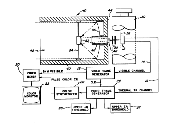
Figure 1 illustrates a schematic block diagram of a
composite visible/thermal-infrared imaging system in
accordance with the invention. As shown, the system may
comprise an optical system 10 for receiving visible and
infrared radiation from an object or a scene and for
focusing the radiation onto a multispectral detector 12
which may provide output signals on two separate
_ 5 _
lZ~3476
RD 16,009
channels 14 and 16 corresponding, respectively, to the
visible radiation and to the thermal-infrared ~IR)
radiation. The output signals on the first channel,
which correspond to the visible radiation impinging on
the detector, may be supplied to a first video frame
generator 18 which formats the raw signals from the
detector into grey scale black and white (B/W) image
frames and outputs a corresponding B/W video signal. The
video output signals from video frame generator 18 may
be supplied to a conventional video mixer 20 and then to
a conventional color monitor 22 to display a visual
image of the scene or object. Similarly, the raw signals
on the second cha~nel of the detector, which correspond
to the infrared radiation impinging on the detector, may
be supplied to a video frame generator 24 which converts
the raw signals to grey scale black and white video
signals which are synchronized with the video signals
from frame generator 18.
Video frame generator 24 preferably includes an
adjustable background threshold offset control 26, which
enables adjustment of the lower sensitiv~ty threshold of
the infrared channel to a preselected value. This
control advantageously allows low ambient temperature
objects to be eliminated from the infrared display so
that only objects or portions of a scene having
temperatures greate- than the preselected value, i.e.,
producing infrared radiation greater than a preselected
amount, are displayed. m is is convenient for avoiding
cluttering of the resulting composite display. The video
frame generator may also include a second background
threshold control 27 for setting an upper cutoff level
so that objects or portions of the scene having
temperatures greater than another preselected value may
lZ834~6
RD 16,009
be eliminated from the display. The two threshold
controls 26 and 27 enable a ~window~ to be set so that
only infrared signals w$thin a preselected range between
the upper and lower threshold limits are displayed. This
S is convenient for enabling objects or portions of a
scene having temperatures within a predetermined
temperature range to be highlighted on the display and
to be easily identified. If desired, multiple threshold
controls may be included to enable multiple infrared
windows to be established.
The output video signal from video frame generator
24 is supplied to a conventional color synthesizer or
color slicer 28 which converts different discrete ranges
of the video signal into different colors to produce a
step-tone false color (or saturated white) video signal
corresponding to a color image of all objects within the
field of view having infrared intensitles above the
selected threshold. The color video signal output from
the color synthesizer is applied to video mixer 20,
where it is combined with the B~W video signal from
video frame generator 18 to produce on color monitor 22
a high resolution composite image. The composite image
comprises a black and white visible image of the scene
or object which is in exact spatial registration with an
overlaid step-tone false color (or saturated white)
thermal-infrared image. The composite image thus
comprises a visual image of the scene or ob~ect which is
highlighted by infrared features with radiance~ between
the preset threshold limits. Of course, either image may
be separately displayed, as well as supplied to other
devices as needed for other purposes.
The video imaging portions of the system of Figure
1 comprising the video frame generators, the color
~;283476
RD 16,009
synthesizer, the video mixer and color monitor, may be
implemented with standard commercially available
devices. BGth video frame generators, for example, may
be substantially similiar and may comprise any
commercially available device capable of producing
standard N~SC or European Pal TV video frame signals.
The background threshold controls 26 and 27 of video
frame generator 24 may simply comprise voltage threshold
controls such that only signals within the preset
threshold range are converted to a video output.
Similarly, color synthesizer 28 may be a commercially
available device which converts the video signal from
frame generator 24 into color video signals.
As will be described in more detail shortly,
detector 12 may comprise a planar spatial array of a
plural$ty of interspersed visible radiation sensitive
and infrared sensitive elements arranged in a matrix.
Each element produces an output in accordance with the
radiation impinging thereon from a corresponding portion
of the scene or the object, which output constitutes one
pixel of the composite im2ge. Detector 12 is preferably
operated at cryogenic temperatures, preferably of the
order of 77 Relvin, for optimum infrared sensitivity.
Accordingly, detector 12 may be disposed within a liguid
nitrogen dewar 30 having windows 32 for admitting
radiation. Alternatively, other cooling schemes, such as
thermoelectric or Joule-Thompson refrigerators, may be
employed for cooling the detector.
Optical system 10 of the system of Figure 1 which
receives radiation and focuses the radiation onto the
detector comprises a wavelength-independent,
non-catadioptric, non-refractive, reflective optical
system. As shown in Figure 1, optical system 10 is
- 8 -
1283476
RD 16,009
preferably a reflective Cassegrain telescope, the
Cassegrain design being advantageous for compactness,
comprising a cylindrical housing 40 having an entrance
opening 42 for the radiation and a closed rear end 44
with a centrally located exit aperture 46 therein. A
cylindrical tubular member 48 may extend inwardly into
the housing from exit aperture 46 as shown. As indicated
in the figure, radiation (indicated by the chain-dotted
lines) entering opening 42 is reflected by an annular
concave primary mirror 50 disposed within the housing
adjacent to end 44 to a convex secondary mirror 52
supported at an intermed~ate location along the axis of
the housing by a support structure 54. Radiation
reflected from the secondary mirror passes through exit
lS aperture 46 and is focused at a common focal plane 56
within the dewar at which detector 12 is located. The
telescope may be focused by a mechanical focusing system
(not illustrated) which moves both the primary and
secondary mirrors ~uch that both the visible and
infrared image~ of the object or scene are brought to a
common focus at the surface of the detector. The primary
and secondary mirrors are preferably coated with gold or
other suitable material which has optimum reflection
char~cteristics at both visible and infrared
wavelengths, preferably throughout the 0.4-14 micrometer
wavelength range. Since the optical system is
non-refractive, its focus is wavelength independent.
~ecause of the widely separated visible and infrared
wavelength bands and the necessity of focusing both the
visible and infrared radiation at precisely the same
focal plane, catadioptric (lens/mirror) and refractive
optical systems are not suitable for the composite
imaging system since the visible and infrared radiation
lZ83476
RD 16,009
would not be focused precisely and the same focal plane,
which would cause problems in producing high resolution
images that are in spatial registration.
Figure 2 illustrates diagrammatically a portion o~ a
hybrid visible/thermal-infrared planar detector array 12
in accordance with the invention. The detector may
comprise a substrate 60 which carries or has formed
therein a plurality of interspersed infrared radiation
responsive elements 62 and visible radiation responsive
elements 64, preferably in alternating rows (or columns)
of infrared elements and visible elements, as shown. As
previously noted, each discrete element responds to the
radiation impinging thereon and produces an output
representative of the radiation emitted from a
corresponding portion of the object or scene within the
field of view of the optical system, and each output
constitutes one pixel of the resulting image. To produce
the visible and infrared images, the elements may be
sequentially scanned by row in a raster format to read
the outputs of successive elements. These outputs
constitute the raw signals which are supplied to the
video frame generators of Figure l to produce the visible
and infrared images. To accomplish this, the detector
array may include generally conventional read-out
circuitry, such as charge coupled devices (CCD's) or
FET's. Figure 2 illustrates diagrammatically a preferred
form of FET read-out circuitry, wherein a dual-gate FET
66 is carried by or formed in substrate 60 for each
detector element 62 and 64. One gate (indicated by line
68) of the FET is connected to an associated row drive
line 70, and the other gate (indicated by line 72) of the
FET is connected to an associated column drive line 74.
The row drive lines 70 may be connected to a
-- 10 --
1~834~76
RD 16,009
row scanner/decoder 76, and the column drive lines 74
may be connected to a column scanner/decoder 78. The
drains ~indicated by lines 80) of the FET's 66
associated with infrared responsive elements 62 in a
column may be connected to a common line 82, while the
drains 84 of the FET's associated with the visible
radiation responsive elements 64 in the colu~n may be
connected to another line 86. Each line 82 may be
connected to a common infrared output line 88 by means
of a gate, such as an FET, 90 which is controlled by the
column scanner/decoder 78. Similarly, each line 86 may
be connected to a common visible output line 92 by means
of a gate or FET 94 which may be controlled by another
column scanner/decoder 96.
Each radiation responsive element is read by
controlling gates 68 and 72 of its associated FET 66 to
turn the FET on. This supplies a voltage corresponding
to the amount of radiation impinging upon the element to
the line 82 or 86 connected to the drain 80 or 84 of the
FET. The row and column scanner/decoders 76 and 78
control the row and column lines 70 and 74 to read
sequentially each successive element, either row-by-row
or column-by-column, for example. The successive outputs
from the infrared radiation responsive elements 62 are
applied to the infrared output line 88 via gates 90, and
the successive outputs from the visible radiation
responsive elements 64 are applied to the visible output
line 92 via gates 94.
Since, in the form illustrated in Figure 2, the
detector comprises alternatinq rows of infrared
radiation responsive and visible radiation responsive
elements (Rows A and C being infrared radiation
responsive and Row B being visible radiation
1~83~76
RD 16,009
responsive), and since the infrared and visible
radiation responsive elements are read out to separate
lines, 82 and 86, respectively, row scanner/decoder 76
may simultaneously activate the row lines 70 associated
s with Rows A and B and column scanner/decoder 78 may
successively step from one column to the next to
simultaneously read out the infrared and visible
radiation responsive elements in Rows A and B of the
same column. This will simplify synchronization of the
visible and infrared signals. The scanner/decoders may
comprise shift registers, for example, which are driven
by outputs from a master clock (CLK). As each stage
turns on, it controls an associated column or row read
line and turns on an associated gate 90 or 94. Also,
although column scanner/decoder 78 is illustrated in
Figure 2 as controlling the column lines of both the
infrared and the visible radiation responsive elements
and a separate column scanner/decoder 96 is illustrated
for controlling gates 94 to output the visible signals,
it will be apparent to those skilled in the art that
column scanner/decoder 78 may also control gates 94,
thus eliminating the need for column scanner/decoder 96.
Furthermore, if desired, column scanner/decoder 96 may
be used for independently controlling a separate column
line connected to the visible radiation responsive
elements. In any event, as will be appreciated, it is
desirable to synchronize the scanning of the elements
and the video frame generators, which may be
accomplished by using a common master clock, for
example. It will also be apparent to those skilled in
the art that while the detector elements of each row of
the detector array of Figure 2 are the same and the rows
alternate, other patterns of detector elements, such as
lZ83476
RD 16,009
a checkerboard pattern, may be used.
Detector elements 62 and 64 are preferably
semiconductor or thin-film elements, and detector array
12 is preferably formed using large scale or very large
scale integration techniques. Since each element
corresponds to one pixel of the composite display, it is
desirable that the detector array 12 comprise a large
number of elements and, of course, that the elements be
made as small as possible to afford a compact device.
The number of elements included in the detector array
will depend upon the desired resolution. Naturally, the
greater the number of elements, the higher the
resolution. Also, the read circuitry comprising FET's
66, gates 90 and 94 and the scanner/decoders may also be
fabricated on substrate 60 as part of the integrated
circuit, as is well known.
Figure 3 is a cross-sectional view of a portion of
a first embodiment of a detector array 12-in accordance
with the invention. In Figure 3 and subsequent figures
which illustrate other embodiments of the detector
array, the read circuitry has been omitted for clarity.
As shown in Figure 3, the detector array may comprise a
P-type silicon substrate having an N-type region 100
therein to form a visible radiation responsive P-N
photodiode 64. ~he infrared radiation responsive
element 62 may comprise a metal silicide-to-silicon
Schottky barrier diode (SBD) formed by depositing a
layer 102 of metal such as platinum on the silicon
substrate and reacting it to form the 8i licide. A
dielectric layer 104, as of silicon dioxide or silicon
nitride, may be deposited on the substrate over the
layer 102 and partially covering the P-N photodiode, as
shown. Metal layer 102 may then be covered with a
1283476
RD 16,009
visible radiation blocking filter 106, as of amorphous
silicon. Amorphous silicon is advantageous as a visible
radiation blocking filter since it can be put down at
low temperatures which will not disturb previously
deposited layers. The P-N photodiode need not be
provided with an infrared radiation blocking filter
since it cuts off at a wavelength of the order of l.l
microns and has no significant infrared radiation
response.
As shown in Figure 3, the detector is adapted to be
illuminated with visible and infrared radiation
(indicated by the arrows in the figure) from the front
side, i.e., from the top in the figure. Photodiode 64
responds to the visible radiation impinging thereon and
produces a corresponding output voltage, and the metal
silicide-to-silicon SBD responds to the infrared
radiation passing through layer 106 to produce an output
voltage in accordance with the radiation impinging on
layer 102.
Figure 4 illustrates a second embodiment of a
detector in accordance with the invention which affords
enhanced Schottky diode efficiency by employing backside
illumination, i.e., through the ~ubstrate. Since a
silicon layer of any substantial thickness will block
vlsible light from reaching the P-N photodiode, the
detector of Figure 4 employs a substrate 110 which is
transparent to both visible and infrared radiation, such
as of sapphire, and a thin epitaxial laye'r of P-type
silicon 112 is deposited on sub~trate 110. An N-type
region is formed in the epitaxial layer to produce a P-N
photodiode 64, and a metal layer 102 is deposited on top
of the epitaxial layer and reacted to form the Schottky
diode. Since silicon becomes transparent at wavelengths
- 14 -
lX83476
RD 16,009
of the order of 2.0 microns, the infrared radiation
passes easily through the sapphire substrate and the
silicon layer 112 to the Schottky diode 62. 9y
appropriately adjusting the thickness of the epitaxial
layer, the visible radiation can be substantially
blocked from reaching the Schottky diode. The bias
voltage of the P-~i photodiode 64 may be adjusted to
control its depletion region and to optimize its
sensitivity to the visible radiation. The disadvantage
of the high dark current levels normally encountered at
room temperature with silicon-on-sapphire structures is
avoided by operating the detector at liquid nitrogen
temperatures of the order previously noted, for
example.
Figure 5 illustrates a third embodiment of a
detector in accordance with the invention, wherein a
conventional P-N photodiode visible radiation detector
array 118 and a conventional Schottky diode infrared
detector array 120 are formed on separate silicon
substrates 122 and 124, respectively, which are placed
back-to-back in a sandwich configuration, as shown in
the figure, with the photodiode array 118 facing the
radiation impinging on the front side of the detector.
me silicon substrates 122 and 124 serve to block
visible radiation from reaching the Schottky diodes 62,
which are formed on .he back side of the detector. If
desired, an additional filter layer 126 of a spectrally
selective material may be included in the sandwich
configuration between the substrates. This allows the
sensitivity and yield of each detector array to be
maximized, although it does result in somewhat higher
packaging complexity and system cost.
1~3476
RD 16,009
Figure 6 illustrates a fourth embodiment of a
detector in accordance with the invention which employs
heterojunction thin-film photoconductive sensors. As
shown in the figure, the infrared radiation responsive
element 62 and the visible radiation responsive element
64 may each be formed as a multilayer structure on a
substrate 130, as of P-type silicon. Each detector may
comprise two thin-film photoconductive layers (132 and
134 for detector element 62, and 136 and 138 for
detector element 64) which are in electrical contact
with each other to form a diode. The lowermost thin-film
layer of each element is in electrical contact with a
metal layer 140 or 142, which serves as one electrode of
the diode, and the uppermost thin-film layers are in
electrical contact with another metal layer 144 or 146,
which forms the other electrode of the diode. Metal
layers 144 and 146, which are the outermost layers and
face the incident radiation, are formed of a material
which is transparent to both the visible and infrared
radiation, such as indium tin oxide. The lower metal
layers 140 and 142 are insulated from substrate 130
except at 150 and 152, respectively, by a layer of
dielectric material 154. The read-out circuitry for the
detector elements, which may be conventional FET devices
such as previously described in connection with Figure 2
or charge coupled devices (CCD's), may be embodied in
substrate 130, and the lowermost metal electrodes 140
and 142 of detector elements 62 and 64 may be in
electrical contact with corresponding read-out devices
160 and 162, respectively at points 150 and 152. (For
simplicity, Figure 6 illustrates only a portion of such
read-out devices 160 and 162.) The uppermost metal
layers 144 and 146 may be connected together to form a
` - 16 -
12~3476
RD 16,009
common terminal for the detector array.
The two thin-film photoconductive layers of each
detector element may be of generally similar but
different materials which are selected to afford a
predetermined barrier height so that the element is
responsive only to radiation within a predetermined
spectral wavelength band, such as visible or infrared,
and such that the element generates photoelectrons which
have sufficient energy to cross the junction and change
the reverse bias on the diode. The read-out devices act
as switches which may be sequentially turned on, as
previously described, to read the amount of
photogenerated charge of each element and reset the
diode reverse bias, similar to reading out a metal
silicide-silicon Schottky diode or a P-N silicon
junction diode. The structure of each detector element
may be similar to the thin-fllm photoconductor
disclosed, for example, in Terui, Y., et al, ~A
Solid-State Color Image Sensor Using
ZnSe-Zn1.xCdxTe Hetero~unction Thin-film
Photoconductor~, IEEE ISSCC 80 Digest of Technical
Papers, p.34-35~ Feb. 1980, except for the selection of
the thin-film materials to give the desired response.
Figure 7 illustrates another form of a
visible/infrared imaging system in accordance with the
invention. The system of Figure 7 differs from that of
Figure 1 in that it employs a detector array 180
comprising elements which are sensitive to both visible
radiation as well as infrared radition, and the detector
array produces time-multiplexed visible and infrared
signals on a single channel, rather than
spatially-multiplexed visible and infrared signals on
different channels. Detector array 180 is preferably
1 ~83476
RD 16,009
front side illuminated and may comprise an array of
Schottky barrier diodes of the type illustrated in
Figure 3, but without the visible radiation blocking
filter layer 106, or the detector may comprise a
conventional bandgap type detector. The visible and
infrared radiation impinging on the detector array may
be time-multiplexed to the detector array by disposing
in front of the detector array a rotating filter wheel
182 having alternating filter segments 184 and 186 which
constitute bandpass filters for transmitting,
respectively, only infrared and only visible radiation.
The output from the detector array may be supplied to a
composite video frame generator and color synthesizer
190, which provides video signals to color display 22.
The rate of rotation of the color wheel may be selected
and synchronized with the composite video frame
generator and the color synthesizer such that a visible
image and an infrared image are displayed as alternate
frames on display 22. As in the system of Figure 1, the
visible image may be displayed as a black and white
image, and the infrared image may be displayed as a
false color image.
While preferred embodiments of the invention have
been shown and described, it will be appreciated by
those skilled in the art that changes may be made in
these embodiments without departing from the principles
and the spirit of the invention, the scope of which is
defined in the appended claims.
-- 18 --