Note: Descriptions are shown in the official language in which they were submitted.
1~83480
--1--
Description
rwo SQUARE MEMORY CELLS
Technical Field
This invention relates to integrated semicon-
S ductor memory circuits and more particularly to a
memory with a very high density of cells, each of
which employs means for storing a binary digit of
information in a trench or groove.
Background Art
Integrated semiconductor memory circuits,
particularly those employing cells which include
essentially a storage capacitor and a switch have
achieved high memory cell densities. One of the
simplest circuits for providing a small dynamic
memory cell i9 described in commonly assigned U. S.
Patent No. 3,387,286, filed July 14, 1967, by R. H.
Dennard. Each cell employs a storage capacitor and
a field effect transistor acting as a switch to
solectively connect the capacitor to a bit/sense
line.
In also commonly assigned U. S. Patents Nos.
3,81i,076 by W. M. Smith, and 3,841,926 by R. R.
Garnache and W. M. Smith, both filed on January 2,
1973, there is disclosed a one device field effect
transistor memory cell of the type described in the
hereinabove identified Dennard patent which utilizes
a layer of doped polysilicon and an N+ diffusion
region in a P type conductivity semiconductor
BU-9-85-032
. - , . . ~, . .
.
'; '
3480
-2-
substrate separated ~y a dielectric medium disposed
on the surface of the semiconductor substrate for
forming the storage capacitor of the well. The
polysilicon layer extends beyond the storage capaci-
tor to act as a field shield between adjacent cellsby applying a negative bias or fixed negative
potential to the polysilicon layer. The N+ diffu-
sion region of the storage capacitor is formed by
using a doped segment of an insulating layer dis-
posed on the surface of the semiconductor substrateand outdiffusing the dopant into the substrate.
Although the cells described hereinabove do
provide memories having a high density of cells in a
planar or two dimensional arrangement, yet each cell
lS does require a significant given area of semiconduc-
tor substrate surface. To reduce the size of the
given surface area for each cell, structures have
been made wherein a semiconductor device or a cell
is formed in a three dimensional arrangement. In
commonly assigned U. S. Patent 4,295,924, filed on
December 17, 1979 by R. R. Garnache and D. M.
Kenney, there is disclosed a semiconductor device
located within a groove or trench with a self-
aligned conductive layer formed on a wall of the
trench either directly or on a supporting insulating
layer as an element of the device. A memory cell
formed in a groove or trench is described in commonly
assigned U. S. Patent No. 4,335,450, filed on
January 30, 1980, by D. R. Thomas, wherein there is
disclosed a cell having a transistor disposed on a
sidewall of a groove or trench with the storage node
disposed below the transistor. Also U. S. Patent
4,32?,476, filed on November 28, 1980, describes a
vertical cell having the storage capacitor in a well
or trench.
BU-9-85-032
. .
lX83480
Patent Cooperation Treaty (PCT) Publication
No. WO 81/03241, dated November 12, 1981, discloses a one
device memory cell structure wherein the storage capacitor
is disposed in a trench with the switching device and
bit/sense line located at the surface of the substrate.
Furthermore, commonly assigned U.S. Patent No. 4,462,040,
filed on March 30, 1980, by I. T. Ho and J. Riseman, discloses
a one device dynamic random access memory utilizing a trench
having vertical sidewalls with the storage capacitor and the
transfer device located within the trench, and U.S. Patents
No. 4,271,418, filed on October 29, 1979, and 4,225,945,
filed on June 6, 1977, and commonly assigned Canadian Patent
Application having Serial No. 517,130, filed on August 28,
1986, by D. M. Xenney, teach a one device memory cell formed
in a groove or trench with the storage node located at the
bottom of the trench, the bit/sense line at the top of this
structure and the transfer device on the sidewall of the
trench.
U.S. Patent No. 4,222,062, filed on May 4, 1976,
d~scloses a memory cell ~tructure wherein a switching device
is formed near the bottom of a trench with the bit line and
storage capacitor located at a wall of the trench.
Commonly assigned Canadian Patent Application having
Serial No. 534,688, filed on April 14, 1987, by
B. F. Fitzgerald, X. Y. Nguyen and S. V. Nguyen, describes a
dynamic memory cell wherein the switching device is located
at the bottom of the trench, with the storage capacitor and
the bit/sense line being formed along opposite sidewalls of
the trench.
BU9-85-032
1;~83480
-4-
None of the hereinabove cited prior art dis-
closes a memory cell having a semiconductor substrate
surface area of less than four lithographic squares.
Disclosure of the Invention
It is an object of this invention to provide a
memory cell which occupies, along with necessary
isolation means, only two lithographic squares of
the surface of a semiconductor substrate, wherein
one lithographic square is defined by the intersec-
tion of two lithographic lines, each line being of
any given width, e. g., less than a micron, as used
in forming elements of devices in integrated semi-
conductor circuits.
In accordance with the teachings of this
invention, a memory is provided which includes a
semiconductor substrate having a major surface and a
trench disposed therein having a longitudinal axis,
storage means disposed on a given sidewall of the
trench, switching means having a control element and
a current carrying element disposed on the given
sidewall of the trench between the storage means and
the major surface of the substrate and coupled to
the storage means, a first electrically conductive
line disposed on the given sidewall in contact with
the control element of the switching means and
having a longitudinal axis arranged parallel to the
longitudinal axis of the trench, and a second
electrically conductive line disposed on the major
surface of the semiconductor substrate in contact
with the current carrying electrode of the switching
means and having a longitudinal axis arranged
orthogonal to the longitudinal axis of the trench.
BU-9-85-032
~;~83480
In a particular embodiment of the present
invention, a dynamic random access memory is provided
which includes a semiconductor substrate having a
major surface and a trench formed therein, first and
second spaced apart storage capacitors disposed
along one sidewall of the trench, first and second
spaced apart bit/sense diffusion regions disposed
along the surface of the substrate and a word line
disposed along the one sidewall of the trench
between the first and second capacitors and the
first and second bit/sense diffusion regions. The
memory may further include first and second bit/sense
lines connected to the first and second bit/sense
diffusion regions, respectively, and arranged
orthogonal to the direction of the trench. Further-
more, the memory may include similarly arranged
elements on the opposite sidewall of the trench
connected to the first and second bit/sense lines.
The foregoing and other objects, features and
advantages of the invention will be apparent from
the following and more particular description of the
preferred embodiments of the invention, as illus-
trated in the accompanying drawings.
Brief Description of the Drawings
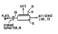
Fig. 1 is a circuit diagram of a dynamic one
device memory cell indicating the principal elements
thereof,
Fig. 2 is a sectional view taken through line
2-2 of Fig. 3 of two dynamic cells of the structure
of the present invention,
BU-9-85-032
lX83480
-6-
Fig. 3 is a plan view of two cells of the
present invention disposed on opposite sidewalls of
a trench,
Fig. 4 is a plan view of a 2x2 array of cells,
each cell being of the type illustrated in Figs. 2
and 3,
Figs. S and 6 are sectional views of the array
illustrated in Fig. 4 taken through lines 5-5 and
6-6, respectively, and
Figs. 7, 8, 9 and 10 are sectional views of the
cell illustrated in Figs. 2 and 3 taken during
~uccessive steps of the process of making the cells.
Best Mode for CarrYinq Out the Invention
Referring to the drawings in more detail, there
is shown in Fig. 1 a basic circuit diagram of a well
known one device dynamic memory cell 10 which
includes a field effect transistor 12 having a gate
14, a storage capacitor 16 having a conductive plate
18 and a storage node 20, and a bit/sense line 22.
A~ is known, to store a binary digit in the storage
capacitor 16, a high or low voltage is applied to
the bit/sense line 22 and the transistor 12 is
turned on to charge the storage node 20 if a high
voltage was applied to the bit/sense line 22,
indicating the presence of, say, a 1 digit, other-
wise the storage node 20 remains uncharged, indicat-
ing the presence of a stored 0 digit. To read
information from the storage capacitor 16, the
bit/sense line 22 is charged to a high voltage
and the transistor 12 is turned on. If the
bit/sense line 22 is discharged, a sense amplifier
~not shown) connected to the bit/sense line 22 will
BU-9-85-032
1~3480
-7-
indicate the presence of a 0 digit in the storage
capacitor 16. If the bit/sense line 22 remains
charged, the storage capacitor 16 is storing a 1
digit.
In accordance with the teachings of this
invention, a novel vertical structure of the memory
circuit of Fig. 1 is illustrated in Figs. 2 and 3,
wherein Fig. 3 is a plan view of the structure and
Fig. 2 is a sectional view taken through line 2-2 of
Fig. 3. As shown in Figs. 2 and 3, two dynamic
memory cells lOA and lOB are disposed on opposite
sidewalls within a trench 24 formed in a semiconduc-
tor substrate 26, preferably made of silicon and
having a P- conductivity. Cell lOA includes the
field effect transistor 12, the storage capacitor 16
and the bit/sense line 22, preferably made of metal
such as copper-doped aluminum, with transistor 12
and the capacitor 16 being located within the trench
24 on a first sidewall thereof and the bit/sense
line 22 being formed on the surface of the substrate
26 in contact with an N+ diffusion region 28 dis-
posed at the surface of the substrate 26, serving as
the drain of the transistor 12. The transistor 12
includes the gate 14, which is preferably made of
P-doped polysiliCon, tungsten silicide (WSi2) or
titanium silicide (TiSi2), or a combination of the
polysilicon and a silicide, or of copper-doped
aluminum, separated from the first sidewall of the
trench 24 by a thin insulating layer 30, preferably
a triple insulating layer made of silicon dioxide,
silicon nitride and silicon dioxide, or a dual layer
made of silicon dioxide and silicon nitride. The
storage capacitor 16 includes the storage node 20
made in the form of an N~ diffusion region disposed
along the first sidewall of the trench 24 and the
conductive plate 18, which may be made of P-doped
BU-9-85-032
1;~83480
--8--
polysilicon including boron, separated from the node
or N+ diffusion region 20 by an insulating layer 32,
preferably also a dual or triple insulating layer
made of silicon dioxide and silicon nitride.
A thick layer of insulation 34 is disposed
between the bottom of the trench 24 and the conduc-
tive plate 18, a layer of insulation 36 is prefer-
ably grown, to a thickness of about 1000 angstroms,
as silicon dioxide on the polysilcon plate 18 so as
to isolate the gate 14 from the polysilicon plate
18, and insulating material 38, preferably polyimide
or a reflowable glass, such as borophosphosilicate
glass, is disposed between the the silicon dioxide
layer 36 and the bit/sense line 22.
lS The second dynamic memory cell 108 is also
located within the trench 24 with its field effect
transistor 12' and storage capacitor 16' being
disposed on the second or opposite sidewall of the
trench 24, with the bit/sense line 22 being common
to both cells lOA and lOB. The second transistor
12' includes the gate 14', which is preferably made
of the same material as gate 14, separated from the
second sidewall of the trench 24 by the thin insulat-
ing layer 30. The storage capacitor 16' includes
the storage node 20' also made in the form of an N+
diffusion region disposed along the second sidewall
of the trench 24 within the semiconductor substrate
26 and the conductive plate 18 separated from the N+
diffusion region 20' by the insulating layer 32. An
N+ diffusion region 28', serving as the drain of the
field effect transistor 12', is connected to the
common bit/sense line 22.
Gates 14 and 14' are portions of first and
second word lines 40 and 40', respectively, which
. ~
BU-9-85-032
3480
extend in a vertical direction along the longitudinal
axis of the trench 24 and orthogonal to the direc-
tion of the bit/sense line 22, as indicated in Fig.
3 of the drawings.
It can be seen from Figs. 2 and 3 that two very
compact one device dynamic memory cells lOA and lOB
are provided on opposite sidewalls of a trench 24
isolated from each other, and from any adjacent
cells, by the thick insulation layer 34, wherein all
elements of the two cells lOA and lOB are located
within a trench 24 except for the bit/sense line 22.
The trench 24 may be made as deep and as wide as
necessary to provide a storage capacitor of desired
size and a transistor of desired switching charac-
teristics. In one arrangement of the structure ofthe present invention, the depth of the trench 24 is
preferably 7 microns, with a width of one micron,
and the width of the channel of the transistors 12
and 12' being one micron, with the length of the
channel being equal to one micron. The layer of
insulation 30 forming the gate insulating medium of
the transistors 12 and 12' has a thickness of about
18 nanometers, with the thickness of the silicon
dioxide layers each being 5 nanometers and the
thickness of the silicon nitride layer being 8
nanometers. The thickness of the dielectric layer
32 of the storage capacitor 16 is preferably 13
nanometers, e. g., 4 nanometers of silicon dioxide,
7 nanometers of silicon nitride and 2 nanometers of
silicon dioxide. The layers of insulation 30 and 32
may also be made of the same continuous materials
and having the same thicknesses. The thick layer of
insulation 34 preferably has a thickness of 200
nanometers. The N+ diffusion regions 20 and 20'
each extend into the substrate 26 about 150 nano-
meters from their respective sidewalls of the trench
BU-9-85-032
1~83480
--10--
24. With a spacing between adjacent cells of an
array of cells along the word line direction equal
to one micron or less and along the bit/sense line
direction, which is orthogonal to that of the word
line direction, equal to one micron or less, the
size of one cell at the surface of the semiconductor
substrate may be made equal to 2 square microns or
less, which is produced when the lithographic line
width is equal to one micron or less. Furthermore,
the capacitance of each of the storage capacitors 16
and 16' versus the capacitance of the bit/sense line
22, assuming 64 cells per bit/sense line, provides a
very desirable transfer ratio of at least 20%.
Fig. 4 is a plan view of an array of cells,
each cell being of the type illustrated in Figs. 2
and 3 of the drawings, wherein like reference
characters refer to similar elements, with two OEells
lOA and lOB aligned in the horizontal direction
along the first bit/sense line 22 and two cells lOC
and lOD aligned in the horizontal direction along a
second bit/sense line 22'. The cells lOA and lOC
are also aligned in the vertical direction along
word line 40 and the cells lOB and lOD are aligned
in the vertical direction along word line 40'. As
is known, each of the word lines 40 and 40' is
connected to word decoder and driver circuits 42 for
selective actuation and each of the bit/sense lines
22 and 22' may be connected to known bit line
decoder, precharge and sense amplifier circuits 44.
Fig. 5 is a sectional view of Fig. 4 taken
through line 5-5 thereof and Fig. 6 is a sectional
view of Fig. 4 taken through line 6-6 thereof to
more clearly show the details of the elements of the
cells lOA, lOB, lOC and lOD of the array.
BU-9-85-032
3348()
--11--
By referring to Figs. 4 and s, wherein Fig. 5
is a sectional view taken orthogonally through the
trench 24 in.an isolation region between storage
nodes of the cells, it can be readily seen that the
thick insulating layer 34 is formed along the
sidewalls and the bottom of the trench 24 and on the
upper surface of the semiconductor substrate 26.
The conductive plate 18 is disposed at the bottom of
the trench 24 on the thick insulating layer 34, and
the word lines 40 and 40~ are disposed above the
plate 18 on opposite sidewalls of the trench 24,
separated from the semiconductor substrate 26 by the
thick insulation layer 34 and from the conductive
plate 18 by the insulation layer 36. The polyimide
lS or BPSG 38 completes the filling of the trench 24.
By referring to Figs. 4 and 6 of the drawings,
wherein Fig. 6 is a sectional view taken parallel to
a sidewall of the trench 24 and through the storage
nodes 20' and the drain regions 28', it can be seen
that the first bit/sense line 22 contacts, in a
self-aligned manner, the drain region 28' of the
cell lOB with its storage node 20' spaced from the
drain region 28' by the length of the channel of
transistor 12', and the second bit/sense line 22'
contacts the drain region 28' of the cell lOD with
its storage node 20' spaced from the drain region
28' of the cell lOD by the length of the channel of
its transistor 12'.
As is known, to write into or read from a
random access memory array as shown in Fig. 4, word
line decoder and driver circuits 42 and bit line
decoder, precharge and sense amplifier circuits 44
of any known type may be used to select any one or
more of the cells lOA, lOB, lOC and lOD. Further-
more, it should be understood that the trench 24 may
.
BU-9-85-032
1283480
-12-
contain hundreds of memory cells along each of the
two sidewalls thereof to which the word lines 40 and
40' may be connected and that hundreds of similar
spaced apart trenches may be arranged parallel to
the trench 24 containing similar memory cells to
which the bit/sense lines 22 and 22' may be connected.
The trenches 24 may be spaced apart by one litho-
graphic line, i. e., by as short a distance as one
micron or less.
Any known process may be used to make the
memory cells of the present invention. In one
particular process, boron ions with an energy of
10 Mev are implanted through a major surface of the
semiconductor substrate 26 to produce a concentra-
tion of lE17 to a depth of about 7 micrometers. The
deep trenches 24 about 7 micrometers deep, in the
silicon substrate 26 shown in Figs 2, 3, 4 and 5 of
the drawings may be formed by known reactive ion
etching techniques, preferably with the use of any
known lithographicly defined silicon dioxide masking
layer. After the trenches 24 are formed, the thick
insulating layer 34 may be deposited within the
trenches 24 and on the surface of the semiconductor
substrate 26. The thick insulating layer 34 is
removed, preferably by any known multilayer or
multilevel photoresist ~MLR) process, including a
non-erodable layer, from selected segments of the
sidewalls of the trenches 24 where the field effect
transistors 12 and 12' and the storage capacitors 16
and 16' are to be formed, as well as along the upper
surface of the substrate 26 for the formation of the
drain regions 28 and 28' of the transistors 12 and
12' as indicated in Fig. 7 of the drawings. The
thick insulation layer 34 is retained at the bottom
of the trenches 24 by blocking the segment of the
thick insulation layer 34 at the bottom of the
BU-9-85-032
1;~8348()
-13-
trenches 34 with a layer of photoresist 46, left in
place by terminating the MLR reactive ion etch
photoresist etching before reaching the trench
bottom, as also indicated in Fig. 7 of the drawings.
S As can be seen in Fig. 8 of the drawings, in the
isolation regions between cells along the sidewalls
of the trenches, the layer of photoresist 46 prevents
the removal of the thick insulation layer 34 during
a wet etch process which removes the unwanted
segments of the thick insulation layer 34. If
desired, the thick insulation layer 34 may be a dual
layer made of grown silicon cioxide and deposited
silicon nitride.
After the thick insulation layer 34 has been
appropriately etched, a layer of doped silicon
dioxide 48, about 20 nanometers thick, is deposited
conformally along the sidewalls of the trenches 24.
Again with the use of a layer of photoresist (not
shown), portions of the doped insulation layer 48 at
the upper regions of the trenches 24 are removed, as
indicated in Fig. 9 at the cell region and in Fig.
10 at the isolation region of the drawings. More
specifically, a preferred processing sequence
includes coating the structure with a planarizing
photoresist which fills the trenches 24, reactively
ion etching the planarized photoresist to the
desired level in the trenches 24, and removing the
doped silicon dioxide 48 from the upper portion of
the trenches 24 using dilute buffered hydrogen
fluoride. With the layer 48 appropriately etched, by
using known drive-in techniques, the dopant, which
is preferably arsenic, in the doped insulation layer
48 is driven into the sidewalls of the trenches 24
to form the N~ diffusion regions or storage nodes 20
and 20', as also indicated in Fig. 9 of the drawings.
As can be seen in Fig. 10 of the drawings, since the
BU-9-85-032
~Z8348~
-14-
thick insulation layer 34 is retained on the sidewalls
of the trenches 24 between the cells, the arsenic is
blocked from entering into the semiconductor sub-
strate 26 at those locations. After drive-in, any
appropriate wet etchant, such as the dilute buffered
hydrogen fluoride, may be used to remove the remaining
segments of the doped insulation layer 48.
With the storage nodes 20 and 20' formed in the
sidewalls of the trenches 24, the gate dielectric
layer 30 and the storage capacitor dielectric layer
32 may be formed sLmultaneously by first growing a
layer of silicon dioxide and then depositing a layer
of silicon nitride, followed by oxidation of the
nitrides to form 2-4 nanometers of silicon dioxide
on top of the nitride. The conductive plate 18 is
formed by depositing doped polysilicon into the
trenches 24 and planarizing the polysilicon at the
surface of the substrate 26. After the polysilicon
is planarized, the polysilicon is removed from the
upper portion of the trenches 24 by appropriate
etching until the upper surface thereof is located
below the upper edge of the storage nodes 20 and
20', as indicated in Fig. 2 of the drawings. The
exposed surface of the polysilicon plate 18 is now
oxidized to form the layer of silicon dioxide 36,
which may be, e. g., 1000 angstroms thick. The
gates 14 and 14' of the transistors 12 and 12',
respectively, may then be formed by depositing
another layer of doped polysilicon over the struc-
ture and reictively ion etching the polysiliconuntil the gates 14 and 14' take on the shape
indicated in Fig. 2 of the drawings. If preferred,
the polysilicon layer may be followed by the deposi-
tion of a layer of tungsten silicide or titanium
silicide and then reactively ion etched to provide a
dual layered gate structure which is more conductive
BU-9-85-032
~83480
-15-
than a gate which is made of only doped polysilicon.
By using reactive ion etching techniques, the
silicon dioxide and silicon nitride layers 30, 32
can be removed from all horizontal surfaces, parti-
S cularly from the drain regions 28 and 28' at thesurface of the semiconductor substrate 26. The N+
drain regions 28 and 28' are formed by implanting
arsenic at S0 KEV and a dose of lE15 per centimeter
square into the exposed surface of the substrate 26.
, 10 If desired, copper-doped aluminum may also be used
to make the gates 14 and 14', but only after the N+
drain regions 28 and 28' have been formed. The
remaining portion of the trenches 24 is filled with
insulating material 38 such as polyimide or a
reflowable glass, e. g., borophosphosilicate glass,
and planarized at the major surface of the semicon-
ductor substrate 26. To form the bit/sense lines 22
and 22', a layer of, preferably, copper-doped
aluminum is deposited over the surface of the
structure and appropriately etched into parallel
lines, as more clearly indicated in Fig.4 of the
drawings.
It should be understood that the gate dielectric
layer 30 may differ from the capacitor dielectric
layer 32 as to composition or thickness, by forming
the gate dielectric layer 30 after forming the
conductive plate 18.
It can be readily seen in accordance with the
teachings of this invention that an improved memory
cell has been provided in a vertical structure
within a semiconductor substrate requiring a very
small cell substrate surface area, i.e., only two
lithography squares, not known in the prior.art, by
forming within a trench or groove the storage means,
3s the switching means and the word line of the cell,
BU-9-85-032
1~834~()
-16-
with the bit/sense line disposed on the surface of
the semiconductor substrate and arranged orthogonal
with respect to the the direction of the word line
or trench.
While the invention has been particularly shown
and described with reference to preferred embodi-
ments thereof, it will be understood by those
skilled in the art that various changes in form and
details may be made therein without departing from
the spirit and scope of the invention.
BU-9-85-032