Note: Descriptions are shown in the official language in which they were submitted.
3484
-- 1 --
METHOD AND APPARATUS FOR CONTROLLED REMOVAL
AND INSERTION OF CIRCUIT MODULES
~chnic~l_Ei~l~
The invention relates to electronic circuit
modules and particularly to a method and apparatus for
removal and insertion of circuit modules from and into
connectors forming part of an electronic circuit
arrangement.
2. ~escription of the Prior AL~
Electronic circuit modules such as circuit
boards and other component carriers are commonly connected
to other circuits by means of a bus and connectors in
which the circuit modules may be inserted. It is well
known that removal of a circuit module from a connector in
an active system may cause arcing at the connector and in
the prior art, switches are mounted on circuit boards to
remove electrical power from the board during removal and
insertion of the board from and into an associated
connector. Circuit boards usually have communication and
interaction with other circuits by means of a backplane
bus arrangement to which connectors are connected. The
abrupt disconnection or connection of power to a board so
connected to the bus tends to cause electrical transients
on the bus. Such a disturbance on the bus is likely to
cause error conditions to occur throughout the circuits
connected to the bus. It is therefore not uncommon to
shut down operations of a whole system when one board has
to be removed or inserted. A problem in prior art systems
is that such a procedure requires a reinitialization of
the complete interconnected system or subsystem and a
restoration of interrupted bus communications when the
power is restored. Clearly, such shutting down and
reinitializing is interruptive and time consuming. It is
,~ ~
1~34~4
-- 2 --
particularly disadvantageous in multiprocessor systems
wherein the several processors function independently and
the system operates normally with certain boards removed.
~mm~ ry~f_~hQ;C~z~n t i On
These and other problems of the prior art are
solved and an advance is made in accordance with this
invention in a system wherein circuit modules are
interconnected by a bus, by inhibiting the operation of
the bus during the period that a module is being inserted
or removed from a connector connected to the bus and
reactivating the bus after the module has been inserted or
removed. In the removal of a module f rom its associated
connector, a switch on the module is operated to provide
an inhibit signal via the associated connector to a
control circuit which inhibits operation of the bus. As
the module is removed from its associated connector, the
inhibit signal is deactivated causing the control circuit
to again enable the bus for the performance of normal bus
functions for the remaining modules of the system.
Similarly, when a module is to be inserted in an
associated connector, the switch on the module will be
positioned such that the inhibit signal is transmitted via
the associated connector to the control circuit. In
response, the control circuit inhibits operation of the
bus. Upon full insertion of the module in the associated
connector, the switch is operated to a second state in
which the inhibit signal to the control circuit is
deactivated. As a consequence, the control circuit again
enables the bus to perform normal operations.
Advantageously, this procedure causes at most a
transmission delay for other circuits attempting to
transmit over the bus during the idled periods but does
not in any way interfere with any other operation of any
of the circuitry connected to the bus. In one particular
embodiment of the invention, the control circuit in
response to the inhibit signal seizes control of the bus
and halts the clock signals which control the operation to
1~34~4
the bus, thus preventing any other circuits fro~ seizing or
transmitting data on the bus. When the inhibit signal is
deactivated, the clock pulses will be restarted and the bus will
again be available to all circuits connected to it.
Advantageously, this arrangement does not interfere with the
operation of any circuits other than those on the affected module
except for possible bus access delays and avoids the necessity of a
lengthy power down and reinitialization procedure.
In one particular embodiment the connectors in which
circuit boards are inserted are each equipped with a pair of extra
length pins at the top and at the bottom of the connector. The
longer pins are connected to the actuator operated switch and this
arrangement assures that contact is made with these pins before
other pins. Furthermore, in one embodiment the switch is a double
throw switch having one connection for sending a power unit
inhibiting signal to the power supply associated with the board and
an opto-isolator connected across the switch. An initial opening
of the switch on a fully inserted board does not affect operation
of the power supply unit since this switch is short circuited by
the opto-isolator. However, after the bus control clock pulses
have been appropriately inhibited, a signal is transmitted by the
control circuit to the opto-isolator, thereby opening the path and
causing the power supply unit to be shut down. When a board is
inserted in a connector, the opto-isolator control signal is set to
such a state that the opto-isolator will be in the open state when
the board is first inserted. Upon complete insertion of the board
and operation of the switch, the power control path will be closed
causing the power supply to provide power to the newly inserted
board.
In accordance with one aspect of the invention there is
provided in combination: a data transmission bus circuit; a
plurality of connectors connected to said bus circuit; clock
circuit means for providing bus access clock pulses to said
connectors; control circuit means connected to said clock circuit
means, to each of said connectors and to said data transmission bus
circuit for controlling access to said bus circuit; and a circuit
module removably inserted in one of said connectors comprising
1~34~4
3a
switch means having a predefined state for transmitting a control
signal via said one connector to said control circuit means when
operated to said predefined state in preparation for removal of
said module from said one connector; said control circuit means
responsive to inhibit said clock circuit means in the presence of
said control signal, thereby preventing access to said bus circuit
form any of said connectors and to enable said clock circuit means
in response to interruption of said control signal upon removal of
said board, thereby allowing access to said bus from said
connectors; whereby access to said bus is inhibited when said
switch means is operated to said predefined state in preparation
for removal of the module and access to the bus is allowed when the
board has been removed and the connection from the switch via said
one connector in the control circuit has been broken.
In accordance with another aspect of the invention there
is provided in an electrical circuit comprising a plurality of
circuit modules, a bus for interconnecting said plurality of
circuit modules, power supply means for supplying electrical power
to said modules, and circuit means for controlling access to said
bus, the method of powering down one of said circuit modules
comprising the steps of: a. transmitting a control signal from said
one module to said circuit means for controlling said circuit
means; b. in response to said control signal, seizing said bus by
said circuit means upon completion of a bus transaction by another
of said plurality of circuit modules; c. controlling said bus to
prevent the transmission of signals between said bus and any of
said plurality of circuit modules; and, d. thereafter,
disconnecting said one circuit module from said power supply means
under control of said circuit means.
Brief Description of the Drawing
The invention may be better understood from the following
detailed description of an illustrative embodiment of the
invention, taken together with the
~;34~4
-- 4 --
drawing in which:
FIG. 1 is a block diagram representation of a
lever actuated switch on a circuit board connected to a
bus and control circuitry for controlling the bus during
insertion and removal of the circuit board
FIG. 2 is a schematic representation of a
connector and a circuit board with a lever actuated
switch;
FIG. 3 is a state diagram of the control
circuitry of FIG. 1.
Detailed ~escription
FIG. 1 is a representation of a multiple
conductor bus 150 and a plurality of circuit boards 101
and 102, as well as control circuitry on circuit
board 103. The boards shown are modules representative of
a number of boards plugged into a backplane and connected
to the bus 150 on the backplane by means of circuit board
connectors as depicted in FIG. 2. The circuit boards
~ connected to the bus 150, will normally include the
2b clrcuitry shown on board 101 as well as nùmerous other
clrcult elements and other connectlons to the bus. The
board~ may, for example, be bus lnterface boards provldlng
an lnterface from processors or controllers to the bus.
The addltlonal connectlons and clrcuits on the boards are
not shown in the drawing,since they are not required for
an understanding of the lnventlon. The bus 150 is vlewed
as a multiple conductor bus which may be a standard bus
such as the well-known Multibus II or the S-100 bus
defined as an IEEE standard. Communlcatlon between the
clrcult boards connected to the bus takes place vla the~e
conductors which will include address lead~ in addition to
data and other control leads. The address leads ln this
particular illustrat~ve embodiment are identifled as
destination ID ~DID) leads 0 through 6. Slnce a number of
units communicate via this bu~, an arbitration scheme is
provided. This may be a well known arbitration scheme
such as, commonly used for example, with the Multibus II
* Trade Mark
484
or the S-100 bus. In this illustrative system, each
circuit board is provided with an arbiter circuit 107
which, by monitoring several bus leads, determines when it
is entitled to bus access. When a circuit has gained
access to the bus it will assert the HOLD lead, which is
one of the control leads of bus 150, to notify other
circuits that the bus is occupied.
The control board 103 is shown as a convenient
arrangement for housing bus control circuitry activated in
connection with the removal and insertion of one of the
circuit boards 101. This control circuitry will normally
be only a part of the circuitry on the board. A DC to DC
converter 105 supplies electrical power to circuit
board 101 in a standard fashion. A similar power supply
connection not shown in the drawing exists for board 103
and other circuit boards connected to the bus.
Shown as part of board 101 in FIG. 1 is a
double-pole, double-throw switch 113, having contacts 114
and 116. This switch is actuated to its open and closed
position by means of a latch 210 shown in FIG. 2. When
the board is fully inserted in its associated connector,
the latch 210 is in the closed position shown in broken
lines in FIG. 2. In this position switch contact 114 is
open and contact 116 is closed. In preparation for
removal of a board from its connector and prior to
insertion of the board into the connector, latch 210 is
operated to the open position, shown in solid lines in
FIG. 2. In the open state of the latch, contact 114 is
closed and contact 116 is open. The closing of the
contact 114 causes a connection to be established between
the ground lead 151 and the MTCHLD lead 153 of the
bus 150. This is equivalent to placing a logical 0 on the
MTCHLD lead. As wiil be discussed further in subsequent
paragraphs, the assertion of this lead is used to initiate
action of the circuitry on the control board 103.
4~4
In the closed state of the latch 210,
contact 116 provides a connection from ground lead 151 to
a control input of the DC to DC converter 105 via control
lead 115. The DC to DC converter is a standard power
supply circuit which is responsive to the state of control
lead 115 and ceases to provide power to the board 101 when
this ground connection via lead 115 is opened. A single
power supply may be provided for each of the boards 101
connected to the bus 150. Alternatively, a shared power
supply may be used which may be disconnected individually
from each of the boards. An opto-isolator 118 is
connected across switch contact 116. The opto-isolator is
a commercially available optical device which may be
electrically controlled to present either an open
electrical circuit or a closed electrical circuit. The
opto-isolator, as will be discussed in subsequent
paragraphs is controlled from the control board 103 and
provides a current path between the terminals of switch
contact 116 when it is opened by operation of the
latch 210 to the open position in anticipation of removal
of the board. A control signal from control board 103
opens the path through the opto-isolator at the
appropriate time.
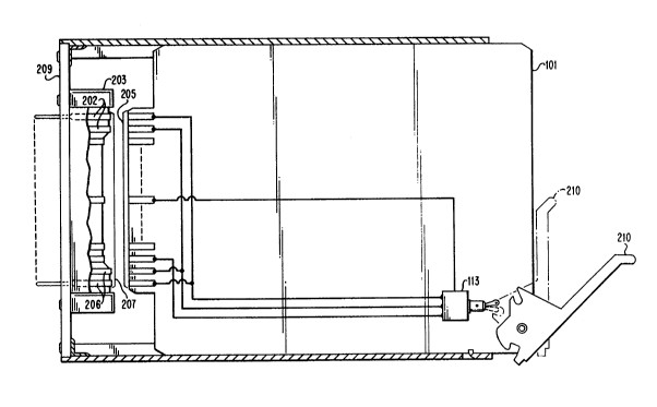
FIG. 2 shows a representation of the circuit
board 101 which may be pluggably engaged with a circuit
board connector 203 shown in a partial cutaway view. A
plurality of contacts 205 on board 101 are arranged to be
engaged with a number of connector pins 207 of the
connector 203. The connector 203 is fastened to a
backplane 209 and pins 207 extend through the backplane
and connections may be made to the pins in a standard
fashion by wire wrap or printed circuitry interconnections
on the backplane. The bus 150 (not shown in FIG. 2)
physically resides on the backplane 209. Circuit
board 101 is equipped with a latch 210 which is shown in
the open or actuated position in solid lines and in the
closed position in dotted lines. The latch operates
4~4
-- 7 --
toggle switch 113, depicted in circuit diagram form in
FIG. 1, to its normal on position when the latch is closed
and to its normal off position when the latch is opened.
The switch 113 is connected by so-called printed wiring
conductors to certain of the contacts 205 and via pins 207
to the backplane 209 when the board is inserted in the
connector 203. The switch 113 further includes the opto-
isolator 118 shown in FIG. 1. FIG. 2 shows that the
uppermost pair of pins 202 and the lowermost pair of
pins 206 of the set of pins 207 is longer, for example one
eighth of an inch longer, than other pins of the
connector. One pin of the upper pair 202 and one pin of
the lower pair 206 are connected to the ground lead 151
(FIG. 1) and the other pins of the two pairs are connected
to the MTCHLD lead 153 (FIG. 1). The corresponding
contacts on board 101 are connected in parallel, as shown
in FIG. 2, and on the backplane 209 as well. The purpose
of the longer pins is to assure that electrical contact is
made between these pins and the corresponding ones of the
contacts 105 before other pins. That assures a proper
sequence of events, as the board is removed or inserted,
as will be discussed later herein.
FIG. 3 is a state diagram representing the
functions of the state machine 120 of FIG. 1 which is part
of the control circuitry on board 103. The sequence of
- functions depicted in FIG. 3 are carried out in connection
with the insertion and removal of a circuit board 101.
State machine 120 consists of sequential logic circuitry
for performing the sequencing function defined by the
state diagram of FIG. 3. It may be readily implemented
using standard logic circuit building blocks. The state
machine 120 receives input signals from the MTCHLD
lead 153, timing circuits 125, 126, and 127, from AND
gate 121 and AND gate 122. It generates control signals
to clock ~ircuit 112, to HOLD lead 157 and to the power
down enable (PRDNEN) lead 155. A control register 123
contains a bit for selectively enabling the AND gate 122.
4~4
-- 8 --
The clock circuit 112 may be any of a number of well-known
clock circuits capable of generating bus clock pulses. In
this illustrative system, two pairs of clock pulses,
CLOCRl and CLOCK2, 90 degrees out of phase are provided on
bus 150 to enable various circuits connected to the bus to
communicate on the bus at the bus clock rate.
Specifically, these clock leads are used in access
circuitry (not shown) in each of the circuits connected to
the bus. Communications on the bus are inhibited under
control of the state machine 120 by inhibiting the CLOCXl
and CLOCR2 leads, thereby preventing access to the bus and
thus isolating the connected circuits from any transients
which may occur on the bus during insertion and removal of
a bus connected circuit board. This inhibiting of the
CLOCKl and CLOCR2 leads will not affect the operations of
other clock circuits tnot shown) on board 103, such as the
clock circuits which control operation of the state
machine 120. Neither does this inhibiting interfere with
other clocked operations on any other bus connected
circuit boards. This feature allows other circuits to
continue to perform functions which do not require bus
access and allows the antire system to resume operation
without reinitialization when the signals on the CLOCXl
and CLOCX2 leads are restored.
As mentioned above, operation of the latch 210
to the open position, which is indicated in solid lines in
FIG. 2, causes switch contact 114 to close and switch
contact 116 to open. If the circuit is fully inserted in
its associated connector, a logical 0 is asserted on the
MTCHLD lead 153 of the bus 150 via switch contact 114 when
the latch is opened. If, on the other hand, the board is
being inserted with the latch in the open poæition, the
signal is applied to the MTCHLD lead when the appropriate
contacts 205 make electrical contacts with either of the
two pairs of long pins 202 and 206 during the insertion
process.
~ 4 ~
The signal on the MTCHLD lead is propagated
through AND 122 if an appropriate enable bit is set in
control register 123. This enable bit is provided to
control the response of the state machine to the MTCHLD
signal. The state machine 120 which is initially in an
idle state represented by block 301 in FIG. 3, responds to
the signal from AND gate 122 by making a transition to
state 1 in block 303 as shown in FIG. 3. Upon entry into
this state, Tl timer 125, which is a 20 microsecond timer,
is initiated and the state machine remains in state 1
until the 20 microsecond period has lapsed. This is done
to avoid starting the process due to transient signals
which may appear on the MTCHLD lead. If the MTCHLD signal
is negated during this period, a return is made to the
idle state. Upon expiration of the 20 microseconds in
state 1, a transition is made to state 2 in block 305. In
this state, the HOLD lead 157 is asserted by the state
machine 120. This is done even though the HOLD lead may
already be asserted by another circuit on the bus, since
the assertion of the HOLD lead by the control circuitry
prevents other circuits from attempting to seize the bus
upon completion by any current user of the bus. The state
machine, however, will not take any action to inhibit the
bus until it has been relinquished by any current user.
To that end, the bus address leads DID0 through DID6 are
monitored by means of AND gate 121. In this illustrative
system, activity on the bus is indicated by a logical '0'
on one of the DID leads. Thus, AND gate 121 provides a
logical '1' output to the state machine on the lead
labeled FREE when the bus is free. Upon the concurrence
of the logical '1' on the FREE lead and an indication that
the MTCHLD lead is still activated, a transfer is made to
state 3, block 306 of FIG. 3. If the MTCHLD lead becomes
deactivated at any time while in state 1, 2 or 3 a return
is made to the idle state. A return is made from state 3
to state 2 if for any reason the FREE lead is negated.
Upon entry in state 3, the T2 timer 126, which is a 1
~34~Li
-- 10 --
microsecond timer, is activated. After 1 microsecond a
transition is made to state 4, block 307 of FIG. 3. The
l-microsecond delay is used to assure that the bus is
indeed free before inhibiting the bus.
In block 307 the bus is inhibited by means of a
stop-clock signal from the state machine 120 to the clock
circuit 112 on conductor 128. This signal results in a
deactivation of the clock pulses on the bus clock leads
CLOCRl and CLOCK2. This deactivation will prevent any
other circuits from responding to transients which may
occur on the bus since the bus access circuitry of any
circuits connected to the bus is dependent on these clock
signals. Subsequent to the generation of the stop-clock
signal, in a subsequent cycle of the state machine, a
transition is made in the state machine to state 5,
block 309, in which a power-down enable signal will be
applied to the PRDNEN lead 155. This signal is applied to
the opto-isolator 118 of board 101, and like opto-
isolators of all circuit boards connected to the bus,
causing each opto-isolator to present an open circuit.
During removal of a board, switch contact 116 will have
been opened by the opening of the latch 210 and thus,
application of the control signal to the associated opto-
isolator causes an open circuit at the switch. Other
boards for which the latches remain closed, will not be
affected by the opening of the opto-isolator devices. For
the board being removed, there is an interruption in the
path from the ground lead 151 to the associated DC to DC
converter power supply 105. This in turn shuts down the
power supply. At this point the board may be removed
without causing arcing or causing unforeseen electrical
transients in the circuitry. During insertion of a board,
the latch 210 and switch contact 116 are in the open
position. Likewise, the opto-isolator is in the open
position and thus, the signal on the PRDNEN lead will have
no effect on the opto-isolator of the board being
inserted.
~ 4~4
The progress from the idle state in block 301
through state block 309, takes less than 200 milliseconds.
Thus, the shutdown of power to a board to be removed takes
place after initial operation of the latch but before the
human operator will have had an opportunity to disengage
the circuit board from its connector. The state machine
remains in the power-down state 5 as long as the MTCHLD
lead remains asserted, that is, as long as there is a path
through the circuit board and switch contact 114. Both
the MTCHLD lead 153 and the GRD lead 151 are connected to
the board via the two pairs of extra long pins 202 and 206
of connector 203. Thus, during board removal, the signal
on the MTCHLD lead is negated only after all other
connector pins have been disconnected from the board.
When a board is being inserted, the latch 210 is closed as
part of the manual board insertion operation.
When that happens, switch contact 114 opens and
switch contact 116 closes. Consequently, the signal on
the MTCHLD lead is negated, and the power supply control
signal i8 asserted on conductor 115, causing the DC to DC
converter 105 to apply power to the newly inserted board
in a standard fashion. Negation of the MTCHLD signal
causes a transition to be made from state 5 to state 6,
block 311 in FIG. 3. A transition may be made back to
state 5 in case of spurious signals on the MTCHLD lead
resulting from the removal of the board. Upon entry into
state 6, a T3 timer 127, which is a 200 millisecond timer,
is initiated. This timer is used to assure that a clean
disconnect has been made in the case of removal of a
board, and to allow sufficient time for power to be
properly applied to the board in the case of board
insertion. Vpon the elapse of this time period a
transition is made to state 7, block 313 in FIG. 3, in
which the HOLD lead 157 of bus 150 is released.
Furthermore, the PRDNEN lead is negated in state 7 thereby
enabling the opto-isolators of all the boards. In a
subsequent cycle of the state machine, a transition is
~ 4 ~4
made to the idle state 301, in which the stop-clock signal
on conductor 128 is released allowing the clock
circuit 112 to again produce the bus clock pulses on leads
CLOCKl and CLOCK2. At this point the bus is available for
use by all of the circuits connected thereto. In the
meantime, however, none of the operations of the other
circuits has been interfered with other than those
resulting from a denial of access to the bus.
It is to be understood that the above-described
arrangement is merely an illustrative application of the
principles of the invention. Various changes and
modifications may be devised by those skilled in the art
without departing from the spirit and scope of the
invention.