Note: Descriptions are shown in the official language in which they were submitted.
DISTRIBUTED PUSH-PUl,L AMPLIFIER
1. Field of the Invention
The present invention relates to a linear electronic amplification system. More
particularly, the invention relates to a system for providing higher efficiency, lower
distortion, and higher power in a distributed amplifier, singly or several in combination.
Il. Back~round of the Invention
For many electronic amplifier applications, it is necessary that the amplifier assembly
10 have wide bandwidth as well as high output power and low signal distortion. For
example, in the field of radio-frequency transmission where low-level radio-frequency
signals are amplified by wide bandwidth linear amplifiers of the distributed type. The
amplified signals are then applied to antenna assemblies for aerial radiation. In these
applications, the output power available from the amplifier must be sufficient to assure
15 that the desired radiated field is achieved. Low distortion, moreover, is required to
assure that the spectral components of the input signal are unmodified in the
amplification process. But, typical amplifier configurations capable of providing the
required wide bandwidth and power, such as the distributed amplifier, also introduce
objectionable distortion.
A distributed amplifier is an amplifier system comprising a number of individualamplifying devices, such as vacuum tubes or solid-state devices. The input terminal of
each amplifying device is connected to an input line, and, correspondingly, the output
terminal of each amplifying device is connected to an output line. The input and output
lines of the distributed amplifying system are so designed as to be lumped-element
25 transmission lines utilizing the parasitic reactive elements, capacitance and inductance,
of the individual amplifying devices as part of the lumped parameters of these lines.
Lumped-element transmission lines are well known in the art and are described in, for
instance, U. S. Patent No. 2,018,320, entitled "RADIO FREQUENCY TRANSMISSION
LINE," to Roberts. Lumped-element transmission lines applied to amplifiers are also
30 described in the prior art in, for instance, U. S. Patent No. 2,930,986, entitled
"DISTRIBUTED AMPLIFIER," to Kobbe et al. In the distributed amplifier, the input
7~
signal to each successive amplifying device is delayed by the delay of the input line, and
the delay of the output line is designed to be identical to that of the input line. This
configuration results in each amplifying device delivering its output signal in phase with
that of the other amplifying devices thereby providing maximum output signal delivered
5 to the load. In effect, the collection of individual amplifying devices operate in parallel.
However, if the amplifying devices were simply connected in parallel, the parasitic
elements, most particularly the input and output capacitances respectively, would
combine in parallel severely reducing the system bandwidth below that available from
a single amplifying device. By including the amplifying devices in a distributed10 amplifier configuration, the effects of the parasitic elements of the amplifying devices
do not add, and the bandwidth of a single amplifying device is preserved in the complete
distributed amplifier system.
In the basic distributed amplifier of the prior art, the operating phase of eachamplifying device is the same with respect to the output, i. e., a positive-going signal at
15 the output terminal of the amplifier system is the result of a positive-going signal at each
amplifying device output. Typically, .he amplifying device produces an output signal
that is asymmetric about the quiescent operating point, for example, the positive output
signal component is somewhat lower in magnitude than the negative output signal
component. This asymmetry is common in Class A operation of amplifying devices such
20 as vacuum tubes, and is very distinct in operating classes of Class AB, Class B and Class
C where the amplifying devices do not amplify the input signal over the complete input
cycle. Such asymmetry results in distortion of the output signal in the basic distributed
amplifier of the prior art.
Distortion in distributed amplifier systems results from the inherent parallel
25 operation of the individual amplifying devices. Operation of a pair of amplifiers in a
push-pull configuration is well known in the art as a means of reducing signal distortion.
A push-pull distributed amplifier system is described in U. S. Patent No. 4,337,439,
- entitled "WIDE BAND AMPLIFIERS," to Sosin. The distributed amplifier system as
taught by Sosin is composed of two individual distributed amplifiers connected in a
30 standard push-pull configuration, i. e., two substantially similar amplifiers are
71~'~
interconnected at their input using a tapped transformer, and interconnected at their
output using a second tapped transformer. Each amplifier must drive the parallelcombination of the load and the output impedance of the companion amplifier. This
typical push-pull configuration results in significant loading of each amplifier by the
5 companion amplifier which reduces the power available for delivery to the load.
Additionally, the required tapped transformers contained in the prior art by Sosin cannot
be effectively fabricated in a manner providing wide-bandwidth performance and
therefore introduce significant losses and frequency limitations. The configuration of
the prior art by Sosin thus additionally results in severe bandwidth limitations over the
10 basic distributed amplifier configuration. Since wide-bandwidth performance and
maximum power delivered to the load are principle features of a distributed amplifier,
a configuration inherently reducing bandwidth and delivered power is undesirable.
The present invention is significantly different from push-pull distributed
amplifiers of the prior art as that taught by Sosin and referenced herein above. The
15 present invention eliminates the companion amplifier loading and allows the required
inverting means necessary for push-pull operation to be fabricated and installed in a
manner consistent with wide-bandwidth performance.
Another variation of a push-pull amplifier in the prior art is described in U. S.
Patent No. 3,571,742, entitled "PUSH-PULL DISTRIBUTED AMPLIFIER," to
20 Wengenroth. The amplifier as taught by Wengenroth is composed of several substantially
standard push-pull amplifiers interconnected to input and output lumped-element
transmission lines of a distributed amplifier configuration. The two individual
amplifying devices in the individual amplifier stages in the configuration by Wengenroth
are connected at their inputs by means of a center-tapped inductor. This center-tapped
25 inductor is effectively an auto-transformer, i. e., a signal is applied to one-half of the
total winding and signal is extracted from the total winding. The auto-transformer
action thus provides equal magnitude and opposed phase input signals to the two
- individual amplifying devices of each individual amplifier as is common in the art of a
standard push-pull amplifier. Similarly, the outputs of the two amplifying devices of
30 each individual amplifier in the configuration by Wengenroth are combined in a
71;~
center-tapped inductor, also effectively an auto-transformer. Thus, each individual
amplifier stage in the configuration by Wengenroth is a substantially standard push-pull
amplifier:two substantially similar amplifying clevices interconnected at their inputs
using a tapped transformer, and interconnected at their outputs using a second tapped
5 transformer. A disadvantage of this configuration by Wengenroth is that the parasitic
elements, particularly input and output capacitance, of the two individual amplifying
devices comprising each amplifying stage are effectively connected in parallel causing
a reduction in bandwidth over that available from a single amplifying device. Another
disadvantage of the configuration by Wengenroth is that the auto-transformer
lO configuration of the input and output tapped inductors results in an electrical
configuration of poor electrical symmetry due to the additional parasitic elements
introduced by the auto-transformer. Thus, the source impedance driving the two input
terminals of the two individual amplifying devices are not equal, and similarly the output
impedance presented to the two output terminals of those amplifying devices are not
15 equal. Such asymmetry results in poor performance over frequency and reduces the
wide-bandwidth capability of the distributed amplifier system. A further disadvantage
of the amplifying system by Wengenroth is that the required tapped inductors cannot be
fabricated in a manner providing wide-bandwidth performance. For example, the
tapped inductors cannot be fabricated with a well defined broadband characteristic
20 impedance, such as 50 ohms or lO0 ohms, since such impedance would present loading
in both the input and output lines of the overall distributed amplifier system. That
loading would make it impossible to properly effect lumped-element input and output
transmission lines of low-loss, wide-bandwidth performance as is necessary for operation
of the distributed amplifier configuration. Still another disadvantage of this
25 configuration is that input and output tapped inductors are needed for each amplifying
stage. The physical size of these tapped inductors and the required position in the circuit
introduce additional parasitic elements (capacitance and inductance) that severely limits
the bandwidth and the total number of stages that may effectively included in the
distributed amplifier system. The principle advantage of the distributed amplifier
30 configuration is the effective use of many individual amplifying stages to provide higher
output power than each single stage while
1~371~
preserving the bandwidth available from a single amplifying stage. Therefore, the
configuration taught by Wengenroth does not allow the principle value of the distributed
amplifier to be realized.
The present invention provides an improved push-pull distributed amplifier
5 system in which individual amplifying devices are arranged in two or more groups. The
amplifying devices within each group operate in phase and groups of amplifying devices
operate 180 degrees out-of-phase with means includea for signal inversions required for
accurate in-phase adding of the output signals of each group. The means utilized in the
present invention for providing the required signal inversions may be fabricated with
10 very well-defined, low-loss, broad-band characteristics accurately matching both the
characteristic impedance and bandwidth performance of the input and output
transmission lines of the distributed amplifier configuration. One such construction of
the signal inverting means is that of a transformer wound with high-quality transmission
line of the impedance required to match the signal line to which it is to be applied.
The present invention is substantially different from distributed amplifiers of the
prior art as taught by Wengenroth and referenced herein above. By Wengenroth, a
plurality of substantially standard push-pull amplifiers are utilized as the individual
amplifying elements of a distributed amplifier configuration. Thus, by Wengenroth,
push-pull operation is provided in each of the individual amplifying devices of a
20 distributed amplifier configuration. In contrast, in the present invention configured with
more than one distributed amplifier, a plurality of individual distributed amplifiers are
combined by the substance of the invention to effect push-pull operation.
The present invention may also be applied to a single distributed amplifier. A
configuration of a single distributed amplifier with only two amplifying devices and
25 further configured according to the present invention may be compared to the individual
amplifying stage by Wengenroth. The individual stage by Wengenroth is electrically a
generally standard push-pull configuration suffering the disadvantages as previously
reviewed herein above. In contrast, the present invention configured with a single
distributed amplifier of only two individual amplifying devices fully retains the
30 electrical properties of the basic distributed amplifier configuration. Therefore, the
present invention effectively incorporates the parasitic elements of both the amplifying
devices and the signal inverting devices in very well-defined and properly terminated
transmission line structures which preserve the very broad bandwidth performance of
the distributed amplifier and in addition provides push-pull operation. Thus, the present
5 invention over Wengenroth, applied to a distributed amplifier with as few as two
amplifying devices, retains all of the advantages of the distributed amplifier
configuration while providing the added advantages of push-pull operation.
This improved configuration provides push-pull operation in a distributed
amplifier configuration without compromise of output power and bandwidth inherently
10 introduced by configurations of the prior art. Further, the number of amplifying
devices that may be effectively employed and the frequency performance of the basic
distributed amplifier is not compromised by use of this improved configuration. This
allows the full benefit of the distributed amplifier configuration to be realized. The
phase-opposed operation of the various amplifying devices with accurate in-phase15 addition of their output signals at the output terminal of a distributed amplifier
configuration as embodied herein is a novel push-pull configuration which provides
lower distortion, higher output power, and thus higher efficiency. Moreover, because
of the unique push-pull configuration of the present invention, some of the power
previously lost due to loading by the companion amplifier, as taught in the prior art, is
20 made available to the load. The present invention thus provides as much as a factor of
two improvement in the output power available from a distributed amplifier as taught
in the prior art. By providing higher available output power,the present invention
provides lower distortion for any specific output power. It is well known that distortion
increases when an amplifier is driven to its maximum output capabilities. Since the
25 amplifier of the present invention, for any specific delivered output power, operates at
lower power level with respect to its maximum capabilities than an amplifier of the
prior art composed of a similar number of amplifying devices, the present invention will
provide lower distortion. Further, for any specific desired maximum output power, the
electrical size of the amplifiers of the present invention may be reduced by a factor of
30 as much as two over the electrical size of the amplifiers required in the prior art. The
71;~
input quiescent operating power of the present invention is therefore reduced over the
prior art for an amplifier configuration capable of a specific maximum output power.
The reduced amplifier quiescent operating power of the present invention therefore
provides increased efficiency. The present invention also provides reduced cost over the
5 prior art for an amplifier of specific maximum output power capability because the cost
and the electrical size of the amplifier are directly related.
SUMMARY OF THE INVENTION
Accordingly, it is an object of the invention to provide a push-pull distributed10 amplifier system which corrects for asymmetric output signal strengths.
Another object of the invention is to diminish power losses resulting from driving
parallel combinations of load and output impedance occurring in previous push-pull
distributed amplifier systems.
Another object of the present invention is to further reduce the power losses and
15 frequency limitations associated with the required combining elements of typical
push-pull distributed amplifier systems.
Another object of the present invention is to provide push-pull operation in a
single distributed amplifier.
Another object of the present invention is to provide push-pull combining of two20 or more distributed amplifiers.
Further objects of the present invention are to provide improved distortion
performance, higher efficiency, and higher output power by means of a novel push-pull
distributed amplifier arrangement.
Additional objects and advantages of the present invention will be set forth in part
25 from the description that follows and, in part, will be obvious from the description or
learned by practice of the invention. The objects and advantages of the invention may
be realized and obtained by the methods and apparatus particularly pointed out in the
appended claims.
The present invention achieves the objects set forth above by means of a novel
30 push-pull arrangement of the individual amplifying means of a distributed amplifier.
1;C~;~71;~
Specifically, ~o achieve lhe objects and in accordance with the purposes of the
invention, as broadly described herein, the invention provides a push- pull distributed
amplifier comprising: a distributed amplifier incorporating two or more amplifying
means; a signal inverting means interconnected into the input line between at least one
5 pair of adjacent amplifying means providing an input stimulus to one or more
amplifying means that is phase-opposed to that input; a signal inverting means
interconnected into the output line between at least one pair of adjacent amplifying
means providing in-phase combining of the in-phase and phase-opposed components in
the output circuit; ancl signal delay means, as required, in the input and output circuits
10 to provide required signal delay in both the input and output circuits. The present
invention may be applied with any operating class including Class A, Class AB, Class B,
and Class C and with all class of operation provides improved performance over that
provided by the prior art.
The accompanying drawings, which are incorporated in and constitute a part of
15 the specification, illustrate a presently preferred embodiment of the invention and,
together with the description, serve to explain the principles of the invention.
BRIEF DESCRIPTION OF THE DRAWINGS
Figure I is a schematic diagram showing a push-pull distributed amplifier system
20 according to the present invention.
Figure 2 is a schematic diagram showing a variation of the push-pull distributed
amplifier system of the present invention utilizing two independent input lines.
Figure 3 is a schematic diagram showing a variation of the push-pull distributed
amplifier system of the present invention utilizing two independent distributed
25 amplifiers.
Figure 4 is a schematic diagram showing a variation of the push-pull distributed
amplifier system of the present invention utilizing two independent distributed
- amplifiers and with independent input lines.
Figure 5 is a schematic diagram showing a variation of the push-pull distributed
30 amplifier system of the present invention utilizing multiple independent distributed
371;~
amplifiers each with independent input lines.
Figure 6 is a schematic diagram showing a variation of the push-pull distributedamplifier system of the present invention utilizing multiple independent distributed
amplifiers with two composite input lines.
Figure 7 is a schematic diagram showing a variation of the push-pull distributedamplifier system of the present invention utilizing multiple independent distributed
amplifiers with cross-coupled inputs.
DESCRIPTION OF THE PREFERRED EMBODIMENT
Reference will now be made in detail to a presently preferred embodiment of the
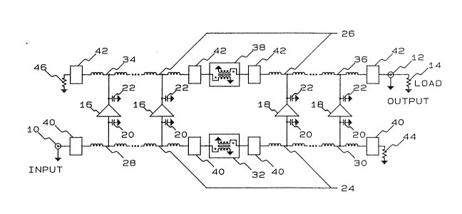
invention, an example of which is illustrated in Figure I of the included drawings. The
purpose of the amplifier of the invention is to amplify an electrical signal applied at the
amplifier input 10 and to deliver the amplified signal to the output terminal 12 and in
turn to a load 14 connected thereto. The load 14 may be any desired entity to which it
15 is desired to deliver signal power. The impedance of load 14 may be resistive, complex,
or totally imaginary. Examples of typical loads include, but are not limited to, an
antenna for aerial radiation, coupling devices for magnetic resonance imaging, and the
induction coils of an induction heating system. The basic amplifier system is of the
distributed type and comprised of a plurality of amplifying devices 16 and 18. Each of
20 the amplifying devices 16 and 18 may be an individual device, example types of which
are common in the art include a vacuum tube, or a solid-state device such as a
Field-Effect Transistor or Bipolar Transistor. Further, each amplifying device 16 and
18 may be comprised of a plurality of components such that each amplifying device 16
and 18 individually comprises a substantially complete amplifier. For example, several
25 vacuum tubes may be configured together in a circuit to form a generally conventional
multi-stage vacuum-tube amplifier, and then in turn applied as the individual
amplifying device 16 and 18 in the present invention. Also, each of the amplifying
devices 16 and 18 is unique and independent with respect to all other amplifying devices
16 and 18. Amplifying devices 16 and 18 may all be of an identical type, or each of a
30 different type, or a combination of several identical types and several different types.
71;~
At least one amplifying device 16 and at least one amplifying device 18 must be included
in the amplifier system of the present invention.
The invention may be applied both to low-power applications and to very
high-power applications. For example, the present invention may be applied using a
5 number of small-signal Field-Effect Transistors to provide increased output power over
that of a single Field-Effect Transistor while preserving wide-bandwidth performance.
Similarly, the invention may be applied using a number of high-power vacuum tubes
also providing higher output power over that of a single vacuum tube while preserving
wide-bandwidth performance. The invention may be applied equally effectively in
10 applications requiring milliwatts of delivered power and those requiring many kilowatts
of delivered power. Further, the invention may be applied with any operating class of
the individual amplifying devices 16 and 18. For example, the individual amplifying
devices may be operated in, but not limited to, Class A, Class AB, Class B, and Class C.
The bandwidth performance is determined primarily by the specific characteristics, such
15 as cutoff frequency, of the individual amplifying devices 16 an 18. Bandwidths in
excess of several hundred megahertz are provided with suitable amplifying devices 16
and 18, example types of which are a broad bandwidth Field-Effect Transistor or broad
bandwidth vacuum tube.
The capacitor 20 is the parasitic input capacitance of each amplifying device 16and 18. The capacitor 22is the parasitic output capacitance of each amplifying device
16 and 18. Whereas the amplifying devices 16 and 18 need not be identical, the input
parasitic capacitances 20 need not be identical and similarly the output parasitic
capacitances 22 need not be identical. An input transmission line 24 and an output
transmission line 26 are constructed incorporating the parasitic components 20 and 22
25 of the amplifying devices 16 and 18 in lumped-element transmission-line configurations
as is common in the art of distributed amplifiers. Such a lumped-element transmission
line is well known in the art and comprises a combination of individual "lumped"- components, such as the output capacitance of amplifying devices 16 and 18, included
in an electronic circuit configuration providing performance similar to a "distributed"
30 element transmission line, such as a coaxial cable, for specific design bandwidths. The
71;~
operation of the lumped-element transmission line is well known in the art and a further
detailed description of operation of the basic lumped-element transmission line will not
be herein repeated. The input line 24 is comprised of two transmission-line segments
28 and 30 interconnected by signal inverting transformer 32. The output line 26 is
5 comprised of two transmission-line segments 34 and 36 interconnected by signalinverting transformer 38. Matching networks 40 in the input line 24 and matchingnetworks 42 in the output line 26 provide impedance matching at the ends of the
transmission-line segments 28, 30, 34 and 36 as is common in the art of lumped-element
transmission line construction. The matching networks 40 and 42 include inductive,
10 capacitive, and resistive components that provide broad-band impedance matching at the
ends of lumped-element transmission lines. Whereas the amplifying devices 16 and 18
need not be identical, the matching networks 40 need not be identical and similarly the
matching networks 42 need not be identical. The signal inverting transformers 32 and
38 are so constructed as to provide the signal delay and bandwidth required. A
15 transmission-line transformer comprised of a length of transmission line, such as coaxial
cable or parallel wire transmission line, formed about a core with each conductor
comprising one winding is one such suitable construction of the signal invertingtransformers 32 and 38 providing broad-band performance. Since the signal inverting
transformers 32 and 38 may be manufactured and installed with very well defined and
20 matched impedance characteristics and with very low- loss, broad-band performance,
the addition of the signal inverting transformers 32 and 38 to the input and output
transmission lines 24 and 26 respectively will not reduce the bandwidth or available
output power of the basic distributed amplifier. Alternately, in applications where very
wide-bandwidth performance is not required, a conventional transformer comprised of
25 primary and secondary windings formed about a core may be used as the signal inverting
transformers 32 and 38. The distributed amplifier is so termed because the amplifying
devices are distributed along the input and output transmission lines 24 and 26
respectively. Since the operating principles of distributed amplifiers are well known in
the art, a further detailed description of the operation of the basic distributed amplifier
30 will not be herein repeated. As referenced herein, a distributed amplifier is understood
71;~
to be an amplifier comprised of a plurality of amplifying devices each with an input
connected to an input line and an output connected to an output line and further where
the input and output lines are constructed utilizing the parasitic elements of the
amplifying devices, matching elements, delay elements, terminating elements, and5 connecting elements providing the broad bandwidth transmission-line configuration for
the input and output lines required for proper operation of a distributed amplifier.
The signal inverting transformer 32 may be interconnected in the input line 24
between any pair of adjacent amplifying devices 16 and 18. Similarly, signal inverting
transformer 38 may be interconnected in the output line 26 between any pair of adjacent
10 amplifying devices 16 and 18. The signal inverting transformers 32 and 38 would
generally be interconnected between the same pair of amplifying devices 16 and 18, but
may be interconnected between uniquely different amplifying devices 16 and 18
providing performance needed in applications that will become apparent by practice of
the invention. Positioning of the signal inverting transformers 32 and 38 between
15 different amplifying devices 16 and 18 provides a practical means of producing a desired
amount of selective distortion of the amplified signal. One such application where
selective distortion would be useful would be in the amplification of an input signal
containing some asymmetry. The signal inverting transformer 32 may be positioned in
the input line 24 and the signal inverting transformer 38 may be positioned in the output
20 line 26 in a manner that produces a controlled asymmetry in the gain characteristic of
an amplifier system of the present invention. That controlled asymmetry may be
introduced in such a manner that it compensates for the asymmetry of the input signal
thereby minimizing distortion in the output signal delivered to the load 14. Since a large
number of amplifying devices 16 and 18 may be included in the present invention, and
25 since one or more signal inverting transformers 32 and one or more signal inverting
transformers 38 may also be included, the present invention provides accurate control
of such selective distortion. When signal inverting transformers 32 and 38 are
interconnected between the same pair of amplifying-devices 16 and 18, the number of
amplifying devices 16 may be equal to or different from the number of amplifying30 devices 18. Balanced performance where positive input signal components and negative
7~:~
input signal components are amplified substantially equally is obtained when signal
inverting transformers 32 and 38 are interconnected between the same pair of amplifying
devices 16 and 18 and the number of amplifying devices 16 equals the number of
amplifying devices 18.
An input signal applied at input terminal 1() travels through input line segment 28
successively delivering input signal in turn to each amplifying device 16 connected to
input line segment 28 as is common in the art of distributed amplifiers. The input signal
is inverted by signal inverting transformer 32. The inclusion of signal inverting
transformer 32 in the input line 24 is novel to the art of distributed amplifiers. The
IO inverted input signal is applied to input line segment 30 where the inverted input signal
is successively delivered in turn to each amplifying device 18 connected to the input line
segment 30. The input signal is finally delivered to input line termination 44 as is
common in the art of distributed amplifiers to prevent detrimental signal reflections in
the input line 24. Since the input transmission line 24 is so designed as to operate as a
transmission line, a terminating resistance 44 properly terminates the input transmission
line 24 providing broad-bandwidth performance. For example, a typical impedance for
the input line 24 would be 50 ohms, and the matched terminating resistance 44 would
then be 50 ohms. A value of terminating impedance may also be chosen that mismatches
the line to which it is applied to provide specific performance, for example,peaking of
the gain at specific frequencies.
The output signals of amplifying devices 16 connected to output line segment 34
sum together in phase to form a single combined signal in the output line segment 34.
A portion of the combined signal in the output line segment 34 is applied to signal
inverting transformer 38. That signal portion is inverted by signal inverting transformer
38 and is applied to output line segment 36 and travels through output line segment 36
to the output terminal 12 and the load 14 attached thereto. Output line segment 36 acts
as a simple transmission line for the signal components from output line segment 34.
The inclusion of signal inverting transformer 38 in the output line 26 is novel in the art
of distributed amplifiers. The output line 26 is reverse terminated by reverse
termination 46 as is common in the art of distributed amplifiers to prevent detrimental
1;C~;~7~ ~
14
signal reflections from portions of the combined output signal in the output line 26 that
are applied to thc output line reverse termination 46. The termination performance of
termination resistor 46 to output line 26 is similar to that provided by termination 44 to
input line 24 as described herein above. A portion of the combined signal of amplifying
5 devices 16 delivered to line segment 34 is communicated to output line reverse
termination 46.
The output signals of amplifying devices 18 connected to output line segment 36
sum together in phase to form a single combinecl signal in the output line segment 36.
A portion of the combined signal in the output line segment 36 is applied to the output
10 connector 12 and load 14 connected thereto. A portion of the combined signal in output
line segment 36 is communicated to the output line reverse termination 46 through signal
inverting transformer 38 and output line segment 34. Signal inverting transformer 38
and output line segment 34 act as a simple transmission line for signal components from
output line segment 36 communicated to the reverse termination 46.
The input signal inverting action of signal inverting transformer 32 in the input
line 24 causes the output signal component of amplifying devices 18 delivered to line
segment 36 to be inverted with respect to the output signal component of amplifying
devices 16 delivered to output line segment 34. Therefore, when the signal of output
line segment 34 is inverted by signal inverting transformer 38 in the output line 26, the
20 two components of output signal delivered to output terminal 12 partly from output line
segment 36 and partly from output line segment 34 inverted by signal inverting
transformer 38, combine in phase delivering a maximum combined output signal to the
load 14.
Since the input signal applied to the amplifying devices 18 is inverted with respect
25 to the input signal applied to amplifying devices 16, the amplifying devices 18 operate
phase-opposed to amplifying devices 16. By means of example, when amplifying devices
18 are being driven so as to source current to output line segment 36, amplifying devices
16 are being driven so as to sink current from line segment 34. Thus, positive output
drive is delivered to the load 14 in part from amplifying devices 18 being driven so as
30 to deliver positive drive to output line segment 36, and in part from amplifying devices
71~
16 being driven so as to deliver negative drive to output line segment 34. Since signal
inverting transformer 38 provides the phase-opposed signals in output line segments 34
and 36 to combine in phase at the output terminal 12, the load 14 attached to the output
terminal 12 is driven in a push- pull manner.
There are many variations and combinations that may be applied to the present
invention, and the invention is intended to encompass all such modifications andvariations as fall within the scope of the appended claims. Several of such variations are
described herein below. Since the present invention allows the use of many individual
amplifying devices 16 and 18, modifications of the connections of the amplifying devices
16 and 18 to the input line 24 and output line 26 may be made to optimize performance
in specific applications. For example, the embodiment of Figure 1 is shown with the
inputs of all amplifying devices 16 connected to input line segment 28 and inputs of all
amplifying devices 18 connected to input line segment 30. Alternately, the input of one
or more amplifying devices 16 may be connected instead to input line segment 30. Similarly, the input of one or more amplifying devices 18 may be connected instead to
input line segment 28. In a similar manner, the outputs of one or more amplifying
devices 16 and 18 may be cross-coupled to output line segments 34 and 36. Such cross-
coupling of the inputs and outputs of one or more amplifying devices 16 and 18 will
provide a desired amount of selective distortion of the amplified signal as referenced
herein above.
For simplicity, the embodiment of Figure I is shown with a single signal inverting
transformer 32 in the input line 24 and a single signal inverting transformer 38 in the
output line 26. Alternately, with reference to Figure 1, substantially similar operation
may be obtained with multiple signal inverting transformers 32 included in the input line
24 and interconnected between various amplifying devices 16 and 18. Multiple signal
inverting transformers 38 may also be included in output line 26 and interconnected
between various amplifying devices 16 and 18. The electrical placement of and the
number of signal inverting transformers 32 would normally be equal to the electrical
placement of and the number of signal inverting transformers 38, but the placement and
number of signal inverting transformers 32 and 38 may be made unequal to provide
71:~
performance needed in applications that will become apparent by practice of the
invention, such as correction of asymmetry of an input signal as referenced herein above.
Since the signal inverting transformers 32 and 38 may be manufactured with
well-defined impedance characteristics and low-loss broad-band performance, the use
5 of multiple signal inversion transformers will not adversely compromise the wide
bandwidth performance of the basic distributed amplifier. However, since the signal
inverting transformers 32 and 38 will exhibit some finite loss, the use of several signal
inverting transformers will reduce the output power available to the load from that
available with a single signal inverting transformer 32 and single signal inverting
10 transforme, 38.
It is apparent to one skilled in the art that the embodiment of Figure I may be
altered so as to include several independent input lines. The number of input lines that
may be included is equal to the total number of amplifying devices 16 and 18. Each
input line would require an input signal. The required input signals may be provided
15 by several different means. For example, a suitable preamplifier system with multiple
outputs of the required phase and signal inversion may be used to provide the needed
multiple input signals. Alternately, the required number of input signals may beprovided from a single input signal by means of a suitable signal divider with input
signal inverting transformers and input signal delay devices included providing the
20 required signal inversion and signal delay. An embodiment according to the invention
is shown in Figure 2 of the included drawings comprising two independent input lines.
With reference to Figure 2, input signals are applied to two input terminals 50 and 52.
These two input signals would normally be identical but may made different to provide
performance needed in applications that will become apparent by practice of the
25 invention. Input signal applied to input terminal 50 is communicated through signal
delay 54, an example type of which is a suitable length of coaxial cable, to input line
segment 28 and delivered to each amplifying device 16 in turn. Line segment 28 is
forward terminated by forward termination 56 to form a complete and independent input
line feeding amplifying devices 16. Input signal applied to input terminal 52 is30 communicated through signal inverting transformer 32 and signal delay 58 to line
;37~
17
segment 30 and is delivered to each amplifying device IB in turn. Input line segment
30 is forward terminated by termination resistor 44 to form a second complete and
independent input line feeding amplifying devices 18. Signal delay 54 and 58 allow
compensation of inherent signal delays to provide proper in-phase summing of theoutput signal components at output terminal 12 and load 14 connected thereto. Input
signal inverting transformer 32 provides signal inversion of the input signal applied to
amplifying devices 18 to provide the push-pull operation of amplifying devices 16 and
18 as previously described herein above. Output signal inverting transformer 38 provides
the in-phase combining of the output signals at output terminal 12 from output line
segments 34 and 36 as previously described herein above. The basic operation of a
distributed amplifier with multiple input lines is well known in the art. The
improvement provided by the present invention is that the present invention provides
push-pull operation of a distributed amplifier with multiple input lines. The push-pull
operation results in improved distortion performance, higher efficiency, and higher
output power over that provided by a distributed amplifier of the prior art with multiple
input lines. The performance of the embodiment of the amplifier shown in Figure 2
with identical input signals is substantially similar to that of the embodiment of the
amplifier shown in Figure I and previously described herein above.
For simplicity, the embodiment of Figure 2 is shown with a single signal inverting
transformer 38 in output line 26. Alternately, multiple signal inverting transformers 38
may be included in the output line 26 interconnected between various amplifying devices
16 and 18. Additionally, embodiments of the present invention comprising multiple
input lines may include one or more signal inverting transformers 32 in one or more of
the multiple inputs.
The embodiment of Figure 2 utilizes signal inverting transformer 32 and signal
delays 54 and 58 as integral elements of the amplifier system. With this configuration,
each of the required individual input signals would normally be similar in phase, delay
and amplitude, although the various input signals may be made different to provide
performance in applications that will become apparent by practice of the invention.
Equal multiple input signals may be provided from a single source by means of a simple
37~:~
18
parallel connection of all of the inputs. Alternately, the multiple input signals and
necessary relative signal inversion and signal delay required with multiple inputs may
be provided by various other means as referenced herein above. An example of another
means for providing the required signal inversion and signal delay for an embodiment
S comprising two input lines, as that of Figure 2, is a preamplifier with two outputs of
opposed phase and specific signal delay. Such a preamplifier may be utilized to supply
the input signals to embodiments substantially similar to that of Figures 2 but with the
signal inverting transformer 32 and signal delay 54 and 58 deleted.
It is further apparent to one skilled in the art that the embodiment shown in
Figure I may be comprised of several independent distributed amplifiers. A
configuration according to the invention comprised of two independent substantially
similar distributed amplifiers is shown in Figure 3. With reference to Figure 3, amplifier
60 is a distributed amplifier but with a connection means 62, an example type of which
is a coaxial connector, added and the input line termination normally connected at the
point of connection means 62 deleted, and amplifier 60 being otherwise unmodified.
Amplifier 64 is a distributed amplifier but with a connection means 66 added and the
output line reverse termination normally connected at the point of connection means 66
deleted, and amplifier 64 being otherwise unmodified.
Output signal inverting transformer 38 is interconnected between the output
terminal 68 of amplifier 60 and connection means 66 of amplifier 64. The combined
assemblage comprised of the output line 70, signal inverting transformer 38 and output
line 72 form a composite output line substantially similar to, with reference to Figure
1, that formed by output line segment 34, signal inverting transformer 38 and output line
segment 36 previously described herein above. A composite line as referenced herein
is understood to be a substantially complete lumped-element transmission line comprised
of two are more individual lumped-element transmission lines, with one or more
terminating means deleted, connected together so as to form one continuous,
- substantially complete lumped-element transmission line.
With reference to Figure 3, input line signal inverting transformer 32 is
interconnected between input terminal 74 of amplifier 64 and connection means 62 of
37~
19
amplifier 60. The combined assemblage comprised of input line 76, signal inverting
transformer 32 and input line 78 form a composite input line substantially similar to,
with reference to Figure 1, that formed by input line segment 28, signal inverting
transformer 32 and input line segment 30 previously described herein above.
The electrical configuration of the amplifier shown in the embodiment of Figure
3 is therefore substantially similar to the embodiment shown in Figure I although the
physical configurations differ. The electrical configurations being similar, the operation
of the amplifier of embodiment of Figure 3 is identical to that previously described
herein above for the embodiment of Figure 1.
For simplicity, the embodiment of Figure 3 is shown with only two independent
distributed amplifiers. Alternately, more than two independent distributed amplifiers
may be incorporated and with one or more signal inverting transformers 32 and one or
more signal inverting transformers 38 included.
It further follows that multiple distributed amplifiers may be incorporated withindependent input signals. Figure 4 of the included drawings shows a configuration
according to the invention comprising two independent distributed amplifiers 60 and 64
and with independent inputs. The electrical performance of the configuration shown in
Figure 4 is identical to that previously discussed herein above with reference to Figure
2.
The embodiment of Figure 4 utilizes signal inverting transformer 32 and signal
delays 54 and 58 as integral elements of the amplifier system. Alternately, the multiple
input signals and necessary relative signal inversion and signal delay required with
multiple inputs may be provided by various other means as referenced herein above.
Since the present invention allows the use of several individual distributed amplifiers,
various different interconnections of the individual distributed amplifiers may be made
to optimize performance in applications that will become apparent by practice of the
invention. One such application is selective distortion as referenced herein above.
- Figure S of the included drawings shows a distributed amplifier system according to the
present invention comprised of several individual distributed amplifiers with
independent input lines for each individual distributed amplifier. Distributed amplifier
71;~
80 is a substantially standard distributed amplifier as referenced herein above.
Amplifiers 64 are distributed ampiifiers but with connection means 66 added and the
output reverse termination normally connected at the point of connection means 66
deleted and distributed amplifiers 64 being otherwise unmodified as referenced herein
5 above. The output lines of the individual dlistributed amplifiers 64 and 80 are
interconnected so as to form a single composite output line as referenced herein above.
Output signal inverting transformer 38 is interconnected in the composite output line
between two adjacent individual distributed amplifiers 64 and 80. For simplicity, Figure
S is shown with only one signal inverting transformer 38, but alternately more than one
10 signal inverting transformer 38 may be interconnected between additional adjacent
distributed amplifiers 64 and 80. When a single inverting transformer 38 is used, it may
be placed between any pair of adjacent individual distributed amplifiers 64 and 80.
Input signal inverting transformers 32 and signal delays 54 and 58 are included in the
embodiment of Figure 5 to provide the required input signal inversion and delay
15 required for proper operation of the amplifier system. The multiple input.signals may
be supplied from a single source by connecting all of the individual inputs together in
parallel as previously referenced herein. Alternately, the required input signal inversion
and delay may be provided by other means, such as a preamplifier with suitable multiple
outputs, with signal inverting transformers 32 and signal delays 54 and 58 deleted as
20 referenced herein above. The operation of the embodiment of Figure 5 is substantially
similar to that of Figure 4 and previously referenced herein.
Further, when the present invention is configured with multiple individual
distributed amplifiers, the input lines may be interconnected to form one or more
composite input lines. An embodiment of the present invention comprising several
25 individual distributed amplifiers and two composite input lines is shown in Figure 6.
With reference to Figure 6, distributed amplifier 60 is a distributed amplifier but
modified by the addition of connection means 62 and deletion of input line termination
- as previously referenced herein. Distributed amplifiers 64 are distributed amplifiers but
modified by the addition of connection means 66 and deletion of output line reverse
30 terminations as previously referenced herein. Distributed amplifier 82 is a distributed
71;~
amplifier but with connection means 62 added and the input line termination normally
connected at the point of connection of connection means 62 deleted, and connection
means 66 added and output line reverse termination normally connected at the point of
connection of connection means 66 also deleted. The output lines of the individual
distributed amplifiers 60, 64, and 82 are interconnected to form a single composite
output line as referenced herein above. The input lines of the individual distributed
amplifiers are interconnected to form two composite input lines 84 and 86. Input signal
inverting transformer 32 and delays 54 and 58 are included in the embodiment of Figure
6 to provide the required input signal inversion and delay required for proper operation
of the amplifier system as previously referenced herein. Alternately, any of the means
previously referenced herein of providing multiple input signals may also be used. The
operation of the embodiment of Figure 6 is substantially similar to that of Figure 4 and
previously referenced herein. For simplicity, a single output signal inverting transformer
38 is shown in the embodiment of Figure 6. When a single inverting transformer 38 is
used, it may be placed between any pair of adjacent individual distributed amplifiers 60,
64, and 82. Alternately, more than one signal inverting transformer 38 may be
interconnected between additional adjacent distributed amplifiers 60, 64, and 82.
Further, when the present invention is configured with multiple individual
distributed amplifiers, the individual amplifiers may be interconnected in a cross-
coupled manner. An embodiment of the present invention comprising several individual
distributed amplifiers and further comprising a cross-coupled input connection is shown
in Figure 7. With reference to Figure 7, individual distributed amplifiers 60, 64 and 82
are substantially standard distributed amplifiers but modified as referenced herein above.
The output lines of the individual distributed amplifiers are interconnected so as to form
a single composite output line as previously referenced herein. The input lines of the
individual distributed amplifiers are interconnected so as to form two independent
composite input lines 88 and 90. Each composite input line 88 and 90 interconnects
several individual distributed amplifiers on one side of inverting transformer 38 and at
least one individual distributed amplifier on the other side of inverting transformer 38.
As previously referenced herein, such cross-coupling provides a means of accurate
7~
22
control of the distortion characteristics of the amplifier system of the present invention
in applications that will become apparent by practice of the invention. When a single
signal inverting transformer 38 is incorporated, it may be placed interconnected between
any pair of adjacent individual distributed amplifiers 60, 64, and 82. Further, more than
5 one signal inverting transformer 38 may be included, and similarly more than two
independent composite input lines may be used. The required multiple input signals
required may be provided by various means as previously referenced herein. The
operation of the embodiment of Figure 7 is substantially similar to that of Figure 4
connected with cross-coupling as referenced herein above.
It will be apparent to those skilled in the art that modifications and variations can
be made to the push-pull amplifier of the invention. The invention in its broader
aspects is therefore not limited to the specific details, representative methods and
apparatus and illustrative examples shown and described herein above. Thus, it is
intended that all manner contained in the foregoing description or shown in the
15 accompanying drawings shall be interpreted as illustrative and not in a limiting sense,
and the invention is intended to encompass all such modifications and variations as fall
within the scope of the appended claims.