Note: Descriptions are shown in the official language in which they were submitted.
~ L8~;
Semiconductor Laser Treatment Unit
Technical Field
The semiconduotor laser -treatment unit of this
invention consists of a laser radiation devics and a
control box which houses a control mechanism used to
control the laser radiation device via a cable. The
said laser radiation de~ice is provided at its tip
with a cap which has a pair of touch sensors in the
vicinity of the emission aperture. I-t also is
provided internally with multiple semiconductor
lasers, and lenses for focusing to a single point
individual laser ~eams radiated in parallel from
these multiple semiconductor lasers, thus formin~ an
optical laser beam used in medical treatment.
Background to the Invention
Previously known semiconductor lassr treatment
devices hav0 been described in, for example, Japanese
Patent Publication (Ibku-kai) Sho 58-86178, 58-89278, and 59-
105445. However, this prior art had the following
defects whi~h needed improvement.
The first problem involved the means of
re~ulating the degree of convergence of the laser
beams emltted from the multiple semiconductor
lasers. In other words, the luminous output of the
: - ' ' - , ;
- :. . , ' ' . ' . , ' . '' ':
~%~I~L186
semiconductor lasers used today is r~stricked To
obtain the intensity o~ beam output required for usc
in medical treatment, multiple semiconductor lasers
have to be oombined, and the laser be~ms from thern
fooused at a partioular point. To achieve this,
laser beams are emi-tted ~rorn multiple semiconductor
lasers, and the output ~eams are aligned in parallel
by the corresponding first lenses, and are made to
fall on the second lens at right angles and at a
specified place on its circumference. Howeverl
because the quality of the laser beam variesJ and
because the laser beam emission position~ ie the
part emitting the radiated beam, may be positioned
slightly higher or lowerJ or further to the ront or
rearJ and the angle o~` laser beam emission variesJ
it is difficult to obtain the desired angle of
incidence of the laser beams without adjusting the
relative positions of the semiconductor laserJ first
lens and second lens. Various adjustments are then
requiredJ such as the positioning of the
semiconductor lasers and the corresponding first
lenses at the specified circumference in relation to
the se~ond lensJ within a precision of several tens
to several micronsJ then aligning the emission
points oP the semioonduotor laser b~ams with the
- :: . , ~ . . .
: .
' ', ' ' ,'' ' ~ ~ :
~L2~4~36
foouses o~ the first lens so that the laser beams
are emitted in parallel at the required dcgree by
the ~irst lens, and at the same time makin~ the
optical axis of the parallel beams radiated ~rom ~he
first lens roughly parallel with the lens axiC3 o~
the first lens ~in other words, the radlation angle
of the beam emitted from ~he ~irst lens - the an~le
Made by the beam axis of the emitted light and the
axis o~ the first lens - is approximately zero~. In
addition when the laser emission point of the said
semiconductor lasers cannot be properly adjusted
with the focuses of the first lenses, and the
optical axis of the parallel beams is slightly
inclined towards the lens axis of the first lenses,
these inclined parallel beams must be made to strike
the second lens at right angles and in a specified
position. BeGause these adiustments have to be made
to within several microns precision, previously
known semiconductor laser treatment devices required
extremely sophisticated techniques, and have the
disadvantage that the semiconductor laser treatment
device is difficult to assemble initiallY, and all
subsequent adiustments during maintenance,
inspection, and replacement of the semiconductor
lasers requlre the device to be returned to the
:
_
:: :
, ~ .
:
i.,. - . .
' ., ' . ~ ' ' ; -
. .
- .- :
'
86
manufacturer for specialist handlin~.
The second disadvanta~e of prior art i~ that
durin~ a power check of the laser beam, there must
be enough space to place a separate power check
uni~ alongside the ~emiconductor laser trea~ment
device. Where no space is available, a separate
table must be provided alongside the semiconductor
laser treatment device, involving some
inconvenience. This method has another disadvantage
in that the results of meter reading will vary
somewhat since the operator is required to make the
final judgement on whether the semiconductor laser
treatment unit is usable or not from the movement of
the meter which con~erts the laser beam to an
eleotric signal.
The third disadvantage is that because the laser
radiation device is operated by hand to radiate
beams using a power chec~ photo-sensor, the operator
radiating the laser beam estimates the central point
of the photo-sensor by eye, leading to laser beams
radiated diagonallY .to the photo-sensor or at
different distances from the photo-sensor. This
causes diPferences in the receiving of~ the laser
beams and thus to variations in the measurements,
giving rise to inconsistencies in the results of
- 4 -
:
'
- ,
. .
,
~28~1186
power cheGks.
Fourthly, to the applicant's knowled~e, prior art
usin~ touch sensors indicate the operation of th0
touch sensor by simultaneously soundin~ a bu~zer or
displaying a larnp whioh shows "In use", EY~n ~hen
the touch sensor is simply in contact with the
patient~s skin and laser beams are not actually
being ernitted, both patients and operators may think
that laser beams are being emitted, thus posing a
problem during treatment.
The fifth problem with prior art is because the
time display which indicates the laser beam emission
time operates by counting backwards from a preset
time to zero, where treatment extends past the
initial preset time and the device is re-operated~
there is no way of calGulating the total emission
time aside from noting the previous emission time on
a piece of paper and addin~ it to the new time.
The ~sixth disadvantage of the prior art is that
because the touch sensor is fixed, some patients
feel an unpleasant sensation when it is pressed on
the treatment area.
Disclosure of the Inven-tion
To solve the problems described above, this
invention consistin~ of a laser radiation device and
-- 5 --
.~ :
.
~L28~:~8~
a control box housing a control mechanism which
controls the laser radiation device via a cable, i~
provided with a cap which has a pair of kouch
sensors in -the vicinity o the laser beam emission
aperture; it also has in~ide it, mul~iple
semiconductor lasers and lenses ~or ~orrnin~ a laser
- beam used for medical treatment by focusing to a
single point the laser beams emitted in parallel
from these multiple semiconductor lasers. The
invention has the following benefits.
The first invention ~the invention described in
item 1 of the Scope of the Claim) is characterized
having a series of first lenses, each
correspondin~ to a semiconductor laser, designed fo,r
making the laser beams emitted from each o ~he
semiconductor las~ers parallel, and a second lens
which collects these multiple parallel beams and
focuses them,to a single point to obtain a treatment
laser beam. Each of these semiconductor lasers is
supported in its own laser holder, these laser holders
fitting closely into multiple insertion holes provided
at specified places on the ciroumference of the body
of the laser radiation de~ice, and corresponding
approximately to the position of inoidence of~ the
laser beams on the seoond lens. Each of these flrst
6 ~ ' '
: : :
~: :
., . . ~, , ~ ,
,
'. ' ' , ~ ~
' ~ ` ~. . . ' ''. - ' `
~2841~3~
lenses is held individually by a lens holder
provided with a suppor-t hole having an inside
diarneter approxirnately equal to the outside diameter
of the first le~s, in a ~lanner such that the
position o~ the first lens oan ~e adiu~ted ~orwards
or backwards within these support hole; this lens holder is
respectively mollnted at the tip of the laser holder
using a screw which passes throu~h the screw hole
constructed in the lens holder and screws into a
female screw at the end of the laser holder. The
s,~id laser holder and a lens holder to~ether form a
subassembly which is attached by fittin~ the laser
holder into the insertion holes in the body of the device.
The position of ~he first lens can be adjusted both ~orwards
and backwards in the support hole, and the position of the lens
holder can be adjusted both horizontally and vertically in
relation to the laser holder by using the n~n~w clearance
provided between the screw and the screw hole. This
permits the semiconductor~1aser and the first lens
to be positioned at several tens or several microns
precision at the circumferences in relation to the
second lensJ simply by fitting the laser holder
tightly into the insertion holes, thus attachin~ it
to the bodY. Secondly, various adiustrnents can be
m,qde in the subassembIy be~ore it is at~ached ~o
-: .
12~ 86
the body of the device; thess include the alignment
of the semiconductor laser emission point and the
focus of ~he first lenses,ie the parallelism of ~he
laser beams from the irst lens and the angle o~
emission o~ beam~ ~rom ~he ~irst lens to be ~dju~ed
by adjusting the mourlt position o~ the lens holder
in relation to the laser holder by altering the
forward/backward position at which the first lens is
held in its support hole and the clearance between
the screw and the screw hole. Thus the laser beams
emitted from the the multiple semiconductor lasers
can be made to converge at the required foc~l point
~or medlcal ~reatment. The replacement of the
semiconductor lasers inYolves simply the replacement
of a pre-adjusted subassemblY body, and ~so oan now
be performed easily and quickly by anyone~ without
special skill ~eing required.
.
~ The second invention (item 2 in the Scope of the
,
Claim~ is characterized bY ~eing provided ~ith a
series of first lenses, each corresponding to a
semiconductor laser and used for making the laser
beams emitted by the semioonductor lasers parallel,
these multiple~laser beams being focused to a sln~le
point by a second lens;whloh oollects ~the beams,~
thus making a laser beam for use in medical
8 - ~
:
: , . ..
.
: .~ . '' -'.;: . ' . ~: ,
~L284:186
treatment; al; the same time, each oP the
serniconductor lasers is h~3ld by individual la~er
holders, these laser holders fitted tightly into
multiple insertion holes provided at specifierl
places on the oirournferenoe whioh oorrsspond ~o the
positions at which the laser beams ~all on the
second lens. Further each of the first lenses is
supported in a lens holder comprising a
rotational body provided with a support hols with an
internal diameter which is approximately equal to
the external diameter of the first lens, and a base
with a curved sur-face hole in which the rotational
body is ~ixed so that it can rotates in all
directions, ~ making the lens self-adjustable
forwards and backwards within the hole. The lens
holder is mounted at the end o~ the laser holder by
a screw which passes through a screw hole in its
base and scre~s into a female screw hole at the end
of the laser holder. The said laser holder and the
lens holder form a subassembly whioh is fixed to the
body when the laser holder is inserted in the
insertion holes; in this subassembly the first lens
oan be adiusted in its support hole and mounted
position of the lens holder can be adjusted
horizontall~ and vertioally in relat~on to the laser
~ 9 ~
". ,, -
,
.
- : . . , . -.
:
128~181~
holder using the narrow clearance between the screw
and the screw hole. Further, by rotating the
rotational body in relation to the base, ~hs beam~
errlitted from the first lens can be made to fall at
right angle~ to the ~eoond len~, and ~hè ~n~le o~
the lens axis of the first len~ can be adjusted in
relation to the lens axis of the second lens. A~ a
result, slanted laser beams ie those beams for which
the first lens was not sufficiently ali~ned with the
semiconductor laser emission point so that the light
beam axis is slightly inclined towards the lens
axisJ can be adjusted so that the laser beams fall
at right angles to the second lens and at a
specified position, simply by lnclinin~ the lens
axis of the first lens whlch is supported by the
rotational body by rotating it ~in relation to the
base. .
In the third invention, the said control
mechanism is constructed of a first control
mechanism and a second control mechanism. The first
control mechanism is characterized by being provided
:
with a radiation control circuit which controls the
emission of the laser beams, a f1xed current clrcuit
which stabilizes the slgnals from the sa1d radiatlon
control circuit, semiconductor lasers which emit
- 10 -
-- ~ ......... . ......... ..
' "~- ~ . .
.: . . : . ~ ,
~2B4~86
laser beams on a signal rom the set current
circuit, an addi-tion circuit which adds the ert~ission
states o the sa;d semiconductor lasers and a touch
switch which goes on when touohed against the humarl
body; the sscond oon~rol mechanism is charaoteriz~d
by having an input processing circuit, a tirne
display circuit, a power check circuit and
radiation laser bea~n check circuit; the input
processing circuit being provided respectivelY with
a first memory circuit which records the on/off
status of the manual switch which starts the output
of laser beams via the radiation control circuit, a
second memory circuit which similarlY records the
on/off status of the stop switch which stops the
laser beam output via the radiation control circuit,
a first AND circuit which is connected to the first
and second memory circuits and calculates the
logical produot of both the manual and stop
switches, a second AND circuit which calculates the
logical product of the first and second memorY
circuits and the touch switch circuit, and an OR
circuit which calculates the logical sum of the
first and second AND circuits; the time display
circuit is provided with a radiation time displa~
lamp which dlsplays the accumulated laser beam
. .
, , ~ .
-, ~
8~a18~E;
emission time calcula~ed by an addition formula
using signals frorn the input processin~ oircui~
givin~ ~he on state of khe rnanual switoh and ~he on
status of -the touoh swi~ch; the time c~lcul~t,ion
cirouit having a radiation time set oircuit which
records a preset time ~nd a preset counter which
adds the laser beam emission time until the preset
time is reached, and halts the emission of laser
beams when ~he laser beam emission time and the
preset counter acoumulated time are equal; the power
check cirouit is provided respectively with a photo-
sensor which receives the laser beams ~rom the
semiconductor laser and converts the optical
intensity of laser beams to an electric signal, a
comparator which acoepts the optical intensity
converted to the said electric signal as a "received
li~ht value" and compares it against a preset
standard value for laser beams; and a radiation
laser beam check circuit which issues a warnin~ of
reduced laser beam output when the result of the
comparison with the signal from the addition circuit
is lower than the standard value. This thus permits
the output intensity of laser beams emltted from the
first control circuit to be checked by the second
control circuit; by radiating a focused laser beam
- 12 -
~' ,
- ' ' ' ..
~Z84~18~
on the photo-sensor which i5 incorporated in ths
power check control circuit, the comparator can
compare the output of the fooused laser beams
received by this photo-sensor with a preset standard
value ~y the cornparator, the result o~ the
comparison bein~ displa~ed selectively in the
control box as a positive or a negative value, thus
providing a fast, easy and accurate power check.
In the fourth invention (Claim (4) in the Scope
of the Claim), a concave housing is formed in the
control bo~, the housing used for a power check and
also approximatelY corresponding to the shape o~ the
cap of the laser radiation device, and further
characterized by being provided on the bottom
surface of the concave housin~ with a photo-sensor
for receiving laser beams, set in a posltion which,
while the laser radiation device is housed,
corresponds to the emission aperture, and is at
right angles to the direction of laser beam
emission. Thus because the concave housing is` made
to correspond approximately to the shape of the cap,
the interior surfaces of the concave housing act as
guides and the laser radiation device is inserted
through its own weight ~shown in lower part of Fig.
9) and cannot be inserted in an incorrect position;
~28~i36
thus -the laser radiation device ~in particular the
cap) is correctly positioned for stora~'e in the
housing regardless of who has been using it In this
posi-tion th0 laser beams are emi-tted on~o -the photo-
sensor, ~hus enablin~ a oheok o~ whether s~u~fî~ent
power is avallable for treatment to be carried out
simply and acourately.
In the fifth invention (described in item (5) in
the Scope of the Claim), the laser radiation device
is oharacterized by having a luminous body in the
cap which li~hts up when it detects some laser beams
emitted from the laser radiation device; the control
box also is provided with a self-illiminating laser
mark which displays laser beam emissions directly
when they are deteoted from the semioonductor la~er,
it also has a time display which uses an addition
formula to calculate the accumulated emission time.
Thus, the cap itself appears to be luminous through
the lighting up o~ the luminous bodY in the laser
radiation device when some laser beams are detected
during laser beam emission, permitting the operator
to tsll that laser beams are being emltted without
releasing his eyes from the treatmen~ area; other
people in the vicinity can also tell that laser
beams are being emi~ted because the laser mark on
- 14 -
' ~ ' ' '
- - ' ~' ' '~
~28~86 27~66-~
~he control box lights up when laser beams are detected from the
laser radiation device. Also since the time dlsplay gives a
display of the accumulated laser beam emission time, the total
radiation time can now be conveniently assessed at a ~lance ev~n
if the time has been reset because of insufficient lnitial
treatment time.
In the sixth invention (item (6) in the Sope of the
Claim), the laser radiation device is characterized by being
provided with touch sensors which are protrudable and retrac~able
:~ 10 in relation to the treatment area. Therefore when pressed against
the treatment area, the touch sensors retract into the cap and
thus do not give the patient nn unpleasant sensation.
According to a seventh aspect of the invention there is
provided a laser radiation device in a semiconductor laser
treatment unit comprising a body being provided internally with
multiple semlconductor lasers and a series of lenses whlch are
used for making the laser beams emitted froD the multiple
semiconductor lasers parallel, and making them converge to a
single point to form a laser beam for medical treatment; each of
the said lenses is constructed to correspond respectively with the
said semiconductor lasers, with Dultiple first lanses used to make
the laser beams issued from the multlple semiconduc~or lasers
parallel, and a second lens which focuses these multiple parallel
laser beams to a sinyle point to form a laser beam used for
treatment; a sub~assembly is formed by the fltting of lens holders
having each one flrst Iens on a 2ront of laser holder having each
:
1 5
:. :
.
., , . ~ :
~Z84186 27G66-3
one semiconduc~or; furkher the multiple insertion hole,s that has a
cross-sectional shape fitted tightly to an outer~circurnferential
shape of the laser holder are opened in the body to correspond
respectively number of the suba~sembly at a ~pecified
circumference on the body, the aircumference approxiwately
corresponding to the po~i-tion o~ lncidence of the la~er beam on
the second lens; and each subassembly is positioned detachably by
the insertion into the insertion hole.
Brief Description of the Drawings
Fig. 1 is an outline side view including a partial cross-
section of the laser radiation device.
Fig. 2 is an outline side view which includes a partial
cross-section of the body only.
Fig. 3 is an outline side view of the body viewed from the
direction of the arrow III in Fig. 2. Fig. 4 is an outline
perspective view of the overall relation between the laser holder,
the lens holder, the screws and the cylindrical lenses used as
"first
15a
. .
.
~28~
lenses".
Figs. 5(a~ through S(d) are descriptive drawin~r
showing alignments of khe semiconductor lasers, the
cylindrical lsnses and the second lensJ the
adiustment relati~n~hip be~,ween the ~emiconduotor
laser bearn ernission point and -their conver~ence on
the cylindrical lens, and the relationship between
the laser beams.
Fig. 6 is an outline perspective view showing the
the lens holder assembly.
Fig. 7 is a circuit diagram showing the probe
circuits incorporated in the control mechanism and
the control circuits.
~ ig. 8 is an overall perspective view of the
semiconductor laser treatment unit.
Fig. 9 is an overall cross-sectional view of the
control box from the direction of the arrow line IX-
IX in ~ig. 8.
Preferred Embodiments of the Invention
The section which follows describes, with
reference to the attached drawings, a series of
embodiments of this invention. The embodiments will
be described as Ernbodiment A,B,C,~, where A is the
first invention, B is the second invention, C is the
third invention, and D corresponds to the fourth,
- 16 -
8~8~;
fifth and sixth inventions re~pectively In this
description, the words "front" and "tip" indic~te
the direction of laser beam emission, while "baok"
indicates the opposite dirsc-tion. Therecre, the
arrow Z in Fig, 4 indicates a Porwards/~aokward~
direction, while -the X and Y direetion~ arrowe~
indicate left/right~ (horizontal) and up/down
~vertical~ directions. Further in the following
descriptions of the embodiments, the comrnon or
similar parts have been given the same code, and any
duplicate description has been omitted.
Embodiment A
The laser radiation device l of this
semiconductor laser treatment unlt is formed from an
outer cover comprisiny a body 2/ a cap 3 which i~
fixed to the front of this body 2, and a cover 4
wh1ch covers the back of the body 2; a clip 5 is
attached~to the bottom part of the body.
The inside of this cylindrical body 2 is provided
with a flange 6, whioh has insertion holes 9 arrayed
at three approximately equal intervals on the
circumference 0 and accurately matching the posi~ion
of incidenee of the laser beam 8 on the seoond lens
7 ldescribed below) on this flange 6. The
cylindrical laser holder 12 1nto whlch the
- 17 -
. ..
.
semiconductor laser 10 is internall~ fixed by a
laser press--fit ring 11, fits closely into these
three insertion holes 9. The tip of this laser
holder 12 has a female sorew hole 13, arld the lerl~
holder 16 i5 rn~llrlted u~ing ths screw 1~ whioh screws
into this female screw hole 13, throu~h -the sorew
hole 15 whioh has a narrow clearanoe in relation to
screw 14. The lens holder 16 and -the laser holder 12
make up a subassernbly 17, with a cylindrical lens 19
being supported as the "first lens" in the support
holes 18 of the lens holder 16. Fur-ther, the front
of the ~lan~e 6 has a stepped part 20 with a flat
convex lens 7 supported as the "second lens" on this
stepped part 20 by a press-fit ring 21. This
semiconduGtor laser treatment unit has therefore, a
semiconductor laser 10, and two linearly arranged
lenses, a cylindrical lens 19 as the "first lens"
and a flat Gonvex lens 7 as the "seoond lens".
The cap 3 has a coned external shapeJ with an
internal passage 22 for laser beams 8.
The inte~rated Gircuits 24 for controlling the
semiconductor lasers 10 are screwed into and held on
the flange 23 at the end of the laser holder 12J
using spacers not shown.
In relation to the emission and focusing of the
:.
- 18 -
.
~28~186
laser beams 8 hy the semiconductor laser ~reatment
unit, the laser beams 8 emitted from thc
semiconductor lasers 10 are first made parallel ~y
the cylindrical lens 19, and then are refr~c~d and
focussed by flat oonvex lens 7 so that they converge
at a point a little past the tip 25 of the oap 3,
thus forming a laser beam used in medical treatrnent.
The optical laser bearns 8 can be focused in this
semiconductor laser treatment unit as follows.
First, before moun-ting the subassembl~ 17 on the
body 2, the parallelism of the optioal beams
radiated from the cylindrical lens 19 can be
adjusted by adjusting the position o~ the
cylindrical lens 19 forwards or backwards in its
holder hole, in the direction of the arrow Z, and
adjusting the emission point P and the focus F of
the cylin~rical lens 19 in the direction of the
arrow Z. Then the mounted position of the lens
holder 16 in relation to the laser holder 16 can be
adjusted by adjusting in the directions of the
arrows X and Yl the clearance between the screws 14
used to mount the lens holder and the screw hole 15,
and the adjusting the emission point P of the
semiconductor laser 10 and the focus point F of th
cylindrical lens 19, in the direction of the arrows
:
-- 19 --
X and Y~ 90 tha-t the radiation angle ie the angle
formed between the optioal axis S of the radiated
beam3 and the lens axis L of the oylindrioal lens
19, is approxirnately zero. Next by inserting the
laser holder 12 in the emission aperture 9 provided
precisely on the oircumference OJ the adjusted
subassembly 17 is attach~d to the body 2 and the
semiconductor laser 10 and the cylindrical lens 19
can be positioned in relation to the flat convex
lens 7 with between several tens and several microns
accurac~.
In other words, this semiconductor laser
treatment unit, firstly enables a semiconductor
laser 10 and a cylindrical lens 19 to be positioned
in relation to a flat convex lens 7 with an accurac~
within the range of several tens of microns to
several micronsJ by simply attaching subassembly 17
to body 2 by fitting laser holder 12 closely into
insertion holes 9. Secondly, prior to mounting the
subassembly 17 on the body 2, the emission point P
of the semiconductor laser 10 and the focal polnt F
o~ the oylindrical lens 13 can be aligned :by
adjusting the parallel emission of the optioal beams
8 using the cylindrical lens 19, :and also adjusting
the angIe of emission of the beams re~racted from
::
- 20 -
~ . ~ , ,: , -
. : ~ . . .
. .
- ' ~
128~
the cylindrical lens 19, by changing the
forwards/backwa~ds position of the cylindrical lens
19 in its support hole and adjustin~ the moun-ted
position of the lens holder 16 on ths l~er holder
12 usin~ the narrow clearance between screw 14 and
the screw hole 15. This perrnits the laser beams 8
emitted from the multiple semiconductor lasers 10 to
be easily focused to the required point of
convergence to produce a laser beam ~or use in
medical treatment. Replacement of the semicond~ctor
lasers 10 involves a simple replacement of the
subassembly, and can be easily and quickly carried
out by anyone without special skills.
Ernbodiment B
The lens holder 26 of the laser radiation device
1 in this semiconductor laser treatment unit is
constructed of a base 27 having screw holes 15, and
a rotational part 29 mounted so that it rotates
freely in all directions, in a curved sur~ace hole
28 provided in the base 27. The cylindrical lens l9
is supported in a support hole 18 in the same way as
in Embodiment A described above, with the addition
of the rotational part 29.
Therefore) in this semiconductor laser treatment
unit, when the em~ssion point P of the
- 21 -
.
~L28~36
semiconductor laser 10 and the focal point F of the
cylindrical len.s 19 oannot be suffioientl~ n~d
and because the optical axis S is leaning ~lightl~
towards the lens axis L, some adius-tment is required
to make the inolined optical beam fall at right
angles and at a specified position on the flat
convex lens 7; this adjustment is now easil~
performed by rotating -the rotational part 29 in the
direction of the arrow ~ towards the base 27, and
inclining the lens axis L of the cylindrioal lens 19
which i5 supported in the lens support hole 18 in
the rotational part 29 towards the lens axis L of
the flat convex lens 7. This iMpro~es the
converg~nce of the laser beams 8 in conjunction with
the first and second actions described for the first
invention above.
In the above explanation of the Embodiments A and
B the adjustment of the cylindrical '`first lens" 19
was described in relation to the directions X,Y,Z
and ~. It is of course possible that no adjustment
is required at all, depending on the quality of the
"semiconductor laser'`. The descriPtion above assumed
that cylindrical lens 19 was to be used as the
'`first lens", but other types of lenses such as a
"flat convex lens".or a '`non-spherical lens" can
~. ,
,:
.~
~2~34~6
also be used; in short, any lens which can be used
to make a laser beam emitted from a semiconductor
laser parallel is suitable. Therefore the ~bove
description could apply e~ually well t~ a "flat
convex lens" or a "non-spherioal lens".
Embodiment C
This semiconductor laser treatment unit has a
control mechanisrn which is provided with a first
control circuit 30 and a second control cirouit 35.
The first control circuit 30 consists of a
radiation control circuit 31, a fixed current
control circuit 32, a semiconductor laser 10, an
addition circuit 34 and a touch switch circuit 37.
The radiation control circuit 31 i5 a circui~ used
to control the emission of laser beams 8 through
operation signals from the second control circuit
35; it thus transmits a stable electric current to
the serniconductor laser 10 via the fixed current
circuit 32. The addition circuit 34 is a circui-t
whic~ adds the electric signals of the "light beams`'
emitted from each o~ the semiconductor lasers 10.
For example, when one of the semiconductor lasers 10
i5 not operating, the calculated electric signal is
lower than the result obtained when all the
serrliconductor lasers are operating. In addition to
- 23 -
128~B6
the "radiation system" for the lassr beaMs 8
comprising the fixed current circuit 32 and the
semiconductor lasers 10~ the first con-trol circuit
is also provided with a separate touch switch
oircuit 37 not shown in the drawin~, whioh ~wi~ohes
ON when i-t touchcs the human body.
The second control circuit 35 is constructed o~
an input processing circuit 38, a time display
circuit 39, a time calculation circuit 40, a power
check circuit 41, a radiation laser beam check
circuit 42 and an alarm circuit 43.
The input processing circuit 38 comprises
primarily a manual switch 44J a first memory
circuit 45, a stop switch 46J a second memory
circuit 47J a first AND circuit 48J a second AND
circuit 43 and an OR circuit 50. The flrst memory
circuit 45 records the ON/QFF status of the manual
switch 44 which~starts the output of laser beams 8
from the said second oontrol circuit; it lS
connected to~the first AND circuit 49 and the second
AND circilit 49. The second memory circuit 47 records
the ON~OFF status of the stop switch 46 which stops
the output o~ the laser beams 8; it is connected to
the first and second AND oircuit9 48~ 49
respectively. Further, the second AND ~clrcuit 49 LS
- 24 - ~ :
: ,
. ~ . . ~ , ..
,
-
~z~
connected 90 that it rsceives si~nals froM kh~ touch
switch circuit ~r~ The first AND circuit 48
calculates the logical product of an on stat~ o th~
m~nual switoh 44 and an o~ state of the ~top switch
46; while the seoond AND cirouit 4~ caloulatss the
logical product of an o~f state of the manu~1 swi-tch
44, an o~f state of the stop switch 46, and an on
state of the touch switch circuit 37. The above
states are transmitted to the OR circuit 50 as
output from the first AND circuit 48 and the second
AND circuit 49 respectivel~J and their lo~ical sum
is calculated. In the second AND circuit, if the
manual switch 44 is on, the on~off state of the
touch switch circuit 3'7 is disregarded. In other
words, whatever its state, and only in this case, if
the manual switch 44 is onl the s-top switch 46 is
off and the touch switch circuit 37 is on, or when
the manual swit,ch 44 is on and the stop switch 46 is
off, a signal indicating emission of laser beams 8
from the input processin~ circuit 38 is transmitted
to the said radiation control circuit 31 and others.
The time display control circuit 39 consists of
an oscillation circuit 51, a total counter circuit
~ and a radiation time display lamp 53. This
circuit uses a calculation formula in the total
- 25 -
.. .. .
-.
~Z8~86
counter circuit 52 to accumulate time in units set
by the oscillation circuit 51 onl~ during radiation
o~ laser beams 8 via signals ~rom the said input
processin~ circuit 38 to switch on the manual swi~ch
44 or switoh on the touoh ~witch cirouit 37. I~
therl displays the total time using a radiation -time
display lamp 53. The total time accurnulated by the
said total counter circuit 52 ie the acoumulated
time of laser beam 8 emission, is initialized onlY
when the total counter circuit 52 is reset.
The time calculation circuit 40 eonsists of a
radiation time set circuit 54 which records a pre-
set time or radiation with laser beams 8, and a
pre-set counter 55 which calculates the radiation
time for laser beams 8 until the set radiation time
in the radiation time set counter 54 is reaohed. In
this time calculation circuit 22, the radiation time
calculated in pre-set counter 55 is compared with
radiation set time, and radiation of laser beams 8
is stopped when the times match.
The power check circuit 41 comprises a "light
receiving element" photo-sensor 56, an amplifier 57~
a comparator 58 and a display part 59. The laser
beam 8 radiated from the said ~emiconductor laser 10
is received by the photo-sensor 56 the stren~th of
- ~6 -
-
,
- . -
~,
- .. :
~28~
the laser beam 8 is assessed as its "intensity"/
converted to an electric signal as a "received light
value", which is khen amplified. In the oomparator
S8, the said "received light value" is comparsd with
a "standard value", a value which in~ioat~ tho
minitnutn volume of laser beams 8 nece~sary for
treatment. The result of the comparison determines
whether the unit can be used or not: if it can be
used, "OK`' is displayed in display part 5g; if not,
"LOW" is displayed in the connected display part 59,
thus permitting the user to determine at a glance
whether the semiconductor laser treatmen-t unit is
suitable for use or not. The incorporation of the
power check circuit ~1 in the second oontrol circuit
35 is an important feature of ~his invention.
The ~rad;iation laser beam check circuit 42 i5
connected~ to the said addition circuit 34 and
comprises~ ~ a comparator 58 which compares the
signals from the addition circui~ 34, and a reduced
output display circuit 61. The comparator 58
contains a preset '`standard vaIue" for the amount of
lase,r beam radiation necessary for treatment, and
continually compares the electric signaIs which
indicates the intensity :of laser beams~8~ in the
those emissions:transtnitted via the a~dition circuit
7~
:
`
,
~4~L8~
34. When the result of the comparison is lower than
the "standard value", ie the output of laser beams 8
being emitted has fallen, this ~act is displa~od ~y
the output reduction displ~y circui-t 61J indicatir~
that the volume of output laser beams 8 has been
reduced to abnormally low levels. Lamps visible to
the eye, or an audible buzzer maY be used for this
output reduction display circuit 61.
The alarm circuit 34 consists of an alarm
generation circuit 62, an amplifier 63 and a speaker
64. When an error is detected in the laser beam 8 or
in any of the aforementioned circuits, that abnormal
signal is received and the alarm generatlon circuit
62 generates an abnormal signal such as lighting up
a lamp and ~ives an alarm via the amplifier 63
through the speaker.
The following describes the use of the
semiconductor laser treatment unit for a `'power
check`'.
When both the manual switch 44 and the stop
switch 46 are on (the touch switch circuit 37 may be
either on or off), a si~nal indicating that emission
of laser beams 8 is possible is transmitted to the
first control circuit 30 from the input proces~sing
circuit 38 via the second AND circuit 49 and the OR
- 28 ~
, , :
'. ~
. . .
~28~6
circuit 50. The first control oircuit 30 cause~
laser beams 8 to be errlitted frorn the seMiconductor
laser 10 through a 5 i~nal transmitted ~ro~tl the
radiation control circui-t 31 to the fixed current
circuit 32. When laser beams 8 are emittcd to ~he
power check circuit 41 incorporated in the second
control circuit 35, the photo-sensor 56 recei~es the
laser bearn 8 and converts the intensity of the laser
beam 8 to an electric signal and then perform~ a
simple "power check`' ~y comparing this received
li~ht value with a preset standard value for laser
beams 8. Because the result of the power check, ie
the result of the comparison of the received light
value and a standard value for laser beams 8, is
displayed as "OK" or "LOW"in the display part 59, it
is easier to tell at a glance whether the unit is
usable or not than with the previous method which
used the oscillation of a meter (not shown~.
Em~odiment D
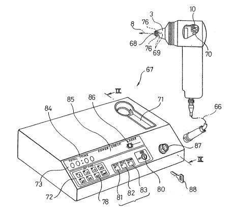
This serniconduct.or laser treatment unit, is
constructed prirnarily of a laser radiation device 1
and a control box 67 connected to the laser
radiation device via a cable 66. An ernission
aperture 68 through which the laser beams 8 are
radiated from the semiconductor laser 10 to the
- 29 -
~289~
outside is provided in cap 3~ and in the vicinity of
the said emission aperture 68 are constructed t,ouch
sensors 69 for de~ecting the treatment area. Th~
touch sensors 69 are a pair of pins which oan detect
that they are in oonta-~t with human bod~ and
separate their ~uides when pressed against the
human skin (treatment area~ (not shown~, permitting
the radiation of laser beams 8 through the guides.
The touch sensors 69 are movable backwards and
forwards using known means such as win~s 76, and
when they are pressed against treatment area and
held there) the touch sensors 69 retract into ~he
inside of the cap 3. This is also one of this
inventionJs ~reat benefits.
Further, a luminous body 70 is provided inside
the laser radiation device 1, this luminous bod~ 70
radiating by sensin~ part of the laser beam 8 from
the semiconductor laser 10. This light hits the cap
3 and is dispersed , causing it to appear from the
outside as if the cap 3 itself is luminescent. This
is used as a clear sign of current "laser emission".
Also beoause the luminous body 70 radiat,es light
when it detects some laser beams 8 from
semiconductor laser 10, it gives an indication of
actual "laser emission". This is another of this
- 30 -
,
12B4~L~6
invention7s lmportant features.
The control box 67 is constructed o-f a conoave
housing 71 used both for holding the laser radia~ion
device 1 and for the power oheok, an oper~iorl panel
72 and a displa~ panel part 73.
The concave housin~ 71 is constructed in the
upper part of the control box 67 as shown in the
cross section drawing Fig. 9, and is also designed
for the power checks. It presents a shape which
almost conforms to the one side o~ the cap 3 of the
laser radiation device. In other words, a oap guide
hole 74 is constructed in the housing in the shape
of the tapering cap 3, and further a photo-sensor56
for receivin~ laser beams is fixed on the bottom
surface part 7.5 correspondin~ to the emission
aperture 68, in a direction at right angles to the
emission direction of laser beams 8. ~hile the laser
radiation device 1 is still housed in this concave
housing 71 before being used for treatment, a power
check can be performed to indicate whether or not
the laser beams 8 have sufficient power for the
treatmen-t. In other wordsJ when laser beams 8 are
emitted from the laser radiation device 1 housed in
the concave part 71, the laser beams 8 hit the
photo-sensor 56 at the bot-tom 75 of the housing, are
,,". ~ :
. ~
~LZ~ 36
converted to an electric signal whioh is
elec-trically checked a~ainst a prese-t ~alue, ancl the
result of the oheok ~either high or low~ i5
indica-ted by the display p~nel 73 a~ either "OK" or
"LO~ uring the power checks, by operating the
switches on the operation panel 72, it is possible
to switch over to use of the touch sensor function
ie the function which permits the emission of laser
beams 8 between the pair of touoh sensors 69 which
are touching the human body ~treatment area~.
The operation panel 72 is Gonstructed of a set
timer 78, operation buttons 79 amd a key switch 80.
The set timer 78 can be used to set the emission
time for laser beams 8 to a value between 5 and 90
seconds, or can be set to continuous use, ie no time
se-t. The operation buttons comprises a reset
button 81, a stop/start button 82 and a manual
button 83. By pressing the reset button 81 twice in
succession, the accumulated emission time o~ laser
beams 8 is totally cleared by an accumulation
circuit ~not shown in the drawing), so that the
accumulated e~ission time of laser beams a can be
re-accumulated from zero.
The stop/start button 82 is a switch which is
used in an emergency to stop the emission cf laser
- . : ,
' ' ', , ~ .
beams 8 bein~ emitted throu~h the touch sen~or
function. When it is pressed the emission o-f laser
heams 8 i5 stopped and a lamp (not shown~ lights up,
The manual bu-tton 8~ is used to start the laser ~eam
OUtptlt check in the "power ohec~". When th~ m~nual
button 83 is pressed, both the said stop/start
button 82 and the manual button 83 light up; if the
stop/start button 82 i5 again pressed at that pointJ
laser beams 8 are emitted and a "power check" is
performed whether the touch sensor funotion is
operating or not (at this point the s~op/start
button will go off). Then if the stop/start button
82 is pressed again~ the emission of laser beams 8
is stopped and the stop/start button 82 lights ups.
The key switch 80 is the power connection
/disconnection switch for the entire semiconductor
laser treatment unit.
The display panel 70 is constructed of~ a time
display 84, a power check displaY 85 and a laser
rnark 86. The time display 84 shows an accumula-ted
display of the accumulated laser beam emission time~
calculated using an addition formula up to a maxirnum
number of 99 minutes 59 seconds. The provision of a
time display 85 which can display the acGumulated
time calculated using an addition formula is one of
1%8~
the features of this invention. The power check
display 85 disPlaYs the characters "OK'` or '`LOW" ~s
a result of the said power check. The laser mark 8
li~hts up while the laser beams 8 are being emitted,
and i5 Ug8d a~s one of the m~thods oP `'warnin~" the
operator and -the surrounding people that laser beams
are being emitted; the abilitY of this invention to
detect the laser beams 8 emitted from the
semiconduc-tor laser 10 and to displa~ laser beam
emission directly is one of its important features.
If a problem occurs durin~ emission of laser beams
8, the characters "CHECK" start blinking in the said
power check display 85, indicating to the operator
that a "power check" is re~uired. 87 is a receptacle
for connection of the cable 66 and 88 is a keY.
The following describes the usage of the
semiconductor laser treatment unit.
Po~er check:
When the laser radiation device 1 is housed in
the concave housing 71, it can be positioned to the
central part of the photo-sensor 56, without
slantin~ the devlce, b~ moving it downwards ~bottom
part of Fig. 9~ with the taPered cap 3 following the
cap ~uide hole 74. This photo-sensor 56 is set, at
the bottom of the concave housing 71 at right angles
- 34 -
''
, .
~Z8~86
to the direction of emission of the laser beams 8,
Therefore, regardless of who has been handling the
laser radiation devioe, it will be stored with tho
emission hole 68 pressed by its own weight and at
ri~ht angle9 a~ainst the pho~o-sensor .~6. So when
the manual button 83 and the stop/start button 82
are pressedJ the laser beams 8 are emitted from the
emission aperture 68 onto the photo-sensor 56,
permitting a "Power check" of whether sufficient
power can be output for treatment. Thus, compared to
previous methods of checking power by applying laser
beams to a hand-held power check photo-sensor 56,
with problems such as the emission aperture 68 being
diagonally positioned, or at different distances, in
relation to the photo-sensor 56, it is now possible
to carry out an accurate and consistent power check.
Also, because the result of the i'power check" is
displayed in characters '`OK" or "LOW" on the Power
check display 85, the usability of the de~ice can be
assessed at a glance.
Radiation of the treatment area by laser beams:
The laser radiation device 1 is taken out uf the
concave housing 71 and plàced a~ainst the treatment
area ~not shown~. At this point the
projectable/retractable touch sensors ~9 are
- 35 -
:
.
~2~6
retracted into the interior of the cap 3, but the
touch sensor function ie the function which permi-ts
the emission of laser beams 8 through the pair o~
touch sensors 69 which are touohing the ph~icn~J s
skin, still operate~, la~er bsaMa 8 can still be
emitted without the touch sensors 69 protrudin~
through the front of the cap 3 to cause any
unpleasant sensation to the patient.
Further , because the luminous body 70 within the
laser radiation device 1, and the laser mark 86 in
the control box 67J immediately light up when they
detect some laser beams 8 from the semiconductor
laser 10, there is an actual indication of "laser
emission", t,hrough a technique which is much safer
than that used in pre~ious art in which the touch
sensor function posted a warning using a lamp or a
buzzer. Further, because the cap 3 itsslf shines
throu~h the action of the luminous body 70, without
removing his eYeS from the treatment area being
treated to look at the laser mark 861 the operator
can identify the emission of laser beams through the
lighted cap, thus improving concentration and safety
during operation.
Also since the accumulated emission time is
calculated by counting the duration of emission of
- 36 -
- ~ .
~az~
laser bearns 8 using an addition formula and is
displayed in the time display 84, the accumulated
emission time can be seen at a glance even when the
time has b~en rese-t because o~ insuf~icien-t emission
for trea~.en-t. This ~ea~ure makes op~ation rnor~
convenient.
Use in IndustrY
This series of inventions has a number of
significant benefits as described above. The
semiconductor laser treatment unit of the first
invention permits the semiconductor laser and the
first lens to be positioned on its circumference in
alignment with the second lens to an accuracy of
several tens to several microns; with the
semiconductor laser and the first lenses so
positioned, it permits the semiconductor laser
emission point and the focus of the first lenses to
be easily aligned, ie the parallel angles of the
laser beams issued from the first lenses, and the
angle of emission of the beams from the first lenses
to be adjusted; and the laser beams emitted from the
multiple semiconductor lasers to be focused to the
degree of convergence required for medical
treatment. Further, because the semiconductor lasers
are replaced by replacing an entire pre--adjusted
- 37 -
.
- .
,, , . . - : .
. .
subassembly) this rePlacement can be performed b~
anyone and no special skills are required.
In the setnioonduotor laser treatment unit o~ the
seoond invention, in addi-tion to tho bene-fits
described above, even when the ssmiconduotor laser
emission point and the focal point o~ the first lens
cannot be suficiently adjusted, and the optical
axis is slightly inclined towards the lens axis, the
inclined beam can be easily Made to hit the seGond
lens at ri~ht angles and at a specified position. In
conjunction with the above benefits, this results in
even better focusing of the laser beams.
In the se~iconductor laser treatment unit of the
third invention, the incorporation of a power check
circuit in the control circuit permits a Power check
to be carried out simply before the start of
treatment, thus avoidln~ the inconvenience of having
a power check unit which is separate from the
semiconductor laser treatment unit. Also, the
usability of the semiconductor laser treatment unit
is displaYed on a display, and can be assessed at a
glance.
The serrliconductor laser treatment unit Df the
fourth invention provides or the laser radiation
devica a concave housin~ with a shape which
- 38 -
.
corresponds to the shape of the cap o~ ~he laser
radiation device, thus permitting -the device to be
stored in an appropriate Position At the bottom of
the concave housing there is a photo~enæor
positioned at ri~ht-angles to ~he direction of laser
beam ernission; this means that regardless of who has
been using it, the laser radiation device is always
pressed into the housing at right angles and by its
own weight, and cannot be placed on a slant or in
the wrong position (distance) in relation to the
photo-sensor. The receiving of laser beams by khe
photo-sensor is therefore uniform and thus enables
an accurate and reproduoible power oheok to be
oarried out. Also because the laser radiation device
is housed in a concave housing, it is protected from
damage and can be managed as one unit in its control
bo~.
.
In the semiconductor laser treatment unit of the
fifth inventlon, because the cap of the
semiconduotor laser itself becomes luminous through
the action of the luminous body whioh emits light
when some laser beams being emitted from the
semiconductor laser are detec~ed, it is possible to
recognize the emission of laser beams without
removin~ one's eYes from t,he treatment area to look
,
- : ,: . .-
- : .,: . .
'- ': ' , .' , ' , :
ï~8~i
at the control box. In addition to the op~rator,
surrounding people can also reoo~nize -that laser
beams are being emitted because a lamp on the
control box lights up. Thereore becau~s people in
t,he vioinitv of the device (the operator and other~
are irnrnediately warned that laser bearns are being
emitted, the safety of the device during actual
laser beam emission is improved. Further, because
the accumulated emission time can be determined at a
glance from the display of a running co~nt of the
laser baam emission time, the total emission time
can be determined easily even if the emission time
is reset because of insufficient treatment time.
In the semiconductor laser~ treatment unit of the
sixth invention, the touch sensors retract into the
cap~ thus avoiding any unpleasant sensation to the
patient even lf the device is pressed a~ainst the
~reatment ar-a.
.
.
.
:
.