Note: Descriptions are shown in the official language in which they were submitted.
12~4'~1~
DISPLAY DEVICE
The present invention relates to a display device, and
particularly but not solely to a liquid crystal display.
It is generally known that the subjection of ferro-electric
liquld crystal displays to long-term electrical potential can
cause degradation of the liquid crystal material (e.g. by ion
migration from the glass substrate) and hence result in
significant deterioration of operation of the display and
reduction in lifetime. Thus, conventionally the data drive is
a bL-polar pulse in phase or in anti-pbase with the bi-polar row
seleCt drive. The leading pulse of a bi-polar signal serves as
an electric potential compensator while the succeeding pulse
swltches the pixel to the desired state.
G.B. Patent specification Publication No.2079509 describes
an arrangement which attempts to cancel the electrical potential
by inverting both the drive voltage and the common electrode
voltage in alternate frames. However oomplete cancellation
throughout the display would occur only if the two frames were
identical, and therefore there can be haphazard patterns of
potential in existence for indeterminate time lengths, causing
random deterioration of the liquid crystal material.
The present invention provides a display device comprising:
means to receive signals representing a plurality of
pictures for display;
a lattice of pixels;
means to address each pixel a number of times for each
picture-signal, the addressing means including means to apply an
.~ ~
~4~
: 2
uni-polar signal to the pixel in accordance with a portion of a
picture-signal appropriate to that pixel
means to determine any net electrical potential value
resultant from the addressing of a pixel for one picture;
means to apply a correction signal to a pixel in accordance
with the output from the determining means.
In this way, the device can operate with a uni-polar pulse
which reduces the time for addressing by one half as compared to
that with a bi-polar pulse, while ensuring that there is no
detrimental effect due to electrical potential. This can be
achieved by ensuring that any potential caused by the uni-polar
pulses are cancelled at the end of each set of addresses
corresponding to a picture-signal for one pixel.
Preferably, the addressing means comprises means to apply
an uni-polar signal to a pixel only when there is a change in
the state of the pixel, and the determining means comprises
means to count the number of changes in state for a pixel during
its addres~ing for one picture-signal. As an electrical
potential is only produced when a change in state of the pixel
occurs, monitoring of the number of changes of state gives an
indication of the net potential existing.
Purthermore, if a pixel is addressed N times during a
picture-signal, where N is the number of bits in each grey level
byte, the difference between the number of l-to-0 changes and
the number of 0-to-1 changes can only be 1 or 0, and the net
electrical potential only +1, -1 or 0 units.
Preferably, the correction means applies, in use, a
correction signal in respect of one address prior to the
initiation of the subsequent address for the next picture.
Preferably, the display device comprises means to store the
output of the determining means appropriate to each of a number
of pixels, and means to pass the stored information to the
correction means to apply a correction signal, advantageously
intermediate that address and the subsequent address.
The present invention also provides a method of operating a
display device having a lattice of pixels the method comprising:
1~4~1~
. ~
: 3
addressing each pixel a number of times for each
picture-signal, includlng applying uni-polar signal to the pixel
in accordance with a portion of a picture-signal appropriate to
that pixel~
determining any net electrical potential value resultant
from the addressing of a pixel for one pictureS
to applying a correction signal to a pixel in accordance
with the output from the determining stage.
Preferably, the method comprises applying an uni-polar
signal to a pixel only when there is a change in the state of
the pixel, and counting the number of changes in state for a
pixel during its addressing for one picture-signal.
Preferably, the method comprises applying a correction
signal in respect of one address prior to the initiation of the
subsequent address for the next picture.
Preferably, the method comprises storing the output of the
determining stage appropriate to each of a number of pixels, and
passing the stored information to the correction stage to apply
a correction signal, advantageously intermediate that address
and the subseguent address.
Preferably, a pixel comprises one or more liquid crystal
cells.
The present invention is applicable to colour displays and
to monochrome displays.
The present invention also embodies eguipment for the
generation, and/or transmission, and/or reception, and/or
processing, of signals suited and/or designed for a display
device as herein defined.
In order that the invention may more readily be understood,
a description is now given, by way of example only, reference
being made to the accompanying drawings, in which:-
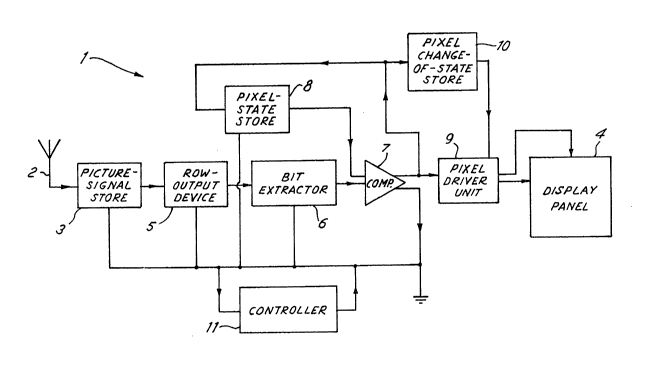
Figure l is a block circuit diagram of a liquid crystaldisplay embodying the present invention;
Figure 2 is a representation of the addressing waveforms
for use in the display of Figure l and
Figure 3 is a representation of the signal input to the
display of Figure 1.
1~4~1~
: 4
In Figure 1, the liquid crystal display unit, generally
designated as 1, has a video signal receiver 2 and a store 3
with a capacity to hold an adeguate amount of the video signals
to enable the display of a complete image, i.e. one picture of
the video signal. The format of the video signal is such as to
provide time-modulation grey-scale addressing of the pixels in a
display panel 4 consisting of a lattice of 600 rows ~ach of 50
bi-stable surface-stabilised ferroelectric liquid crystal
pixel-elements; for one picture, the video signal has four data
bits for each pixel. In this addressing scheme, the lattice is
scanned four times each picture, the setting for each pixel
being in accordance with the appropriate bit, and the time
duration of the pixel in that setting being dependent on the
significence of that bit.
There are four row-output devices (only one, 5, being
shown), each of which enables the video information for a row of
pixels to be taken out of picture store 3: each row-output
device 5 has a bit extractor 6 to separate out one bit of the
information for each pixel of the respective row. The
extractors of the different row-output devices are arranged to
operate on bits of differing significence.
Consider now how the display device 1 operates in relation
to the data bits in one picture signal for a single pixel of
panel 4. Assuming that the least-significent data bit is
already on displa at the relevant pixel in panel 4, then in the
next scan extractor 6 passes the next least significant bit to a
comparator 7 whose other input is connected to a pixel-state
store 8. Accordingly, the new bit-value is compared with the
existing state of the pixel, and comparator 7 passes on an
instructing signal to pixel driver unit 9 only if the state of
the pixel requires changing; in such an eventuality, the driver
unit 9 issues an appropriate monopulse select voltage of the
format shown in Figure 2. Comparator 7 also passes such an
instructing signal not only to pixel-state store 8 in order to
update its record of the display state of the respective pixel,
but also to a store 10 which records the number of changes of
state for each pixel during one picture-signal.
84~1~
s
If comparator 7 determines that this next bit corresponds
to the present state of the pixel, the comparator 7 does not
output an instructing signal to driver unit 9, but only sends a
signal to controller 11 to lndicate the equivalence result of
the comparison test.
This sequence of events is repeated for each of the
remaining bits corresponding to that pixel in the same
picture-signal; thus, once the most-significent bit has been
processed and is being displayed on the panel 4, the
change-of-state store 10 has the net number of changes which the
pixel has undergone in that picture. As the difference between
the number of l-to-0 changes and the number of 0-to-1 changes
can only be 1 or 0 and the net electrical potential on that
pixel only +1,-1 or 0 units, then the value held in store 10 for
that pixel corresponds to the net electrical potential.
Accordingly, controller 11 causes store 10 to output the value
appropriate to that pixel and pass it to driver unit 9 to
produce a compensating pulse (whether positive, negative or
zero) necessary to ensure that there is no net electrical
potential over the entire picture interval. The display
produced by the compensating pulse is cleared immediately the
first data of the next picture is input to the pixel (see Figure
3), and therefore it remains for a period of time which has an
insignificant detrimental effect on the image. ~igure 3
illustrates the position of the compensating pulse C in relation
to adjacent picture-signals wherein, for each display line,
blocks 1,2,3,4 relate to addressing for the least-significent
bit upwards in relation to the first picture-signal, and blocks
lA, 2A, 3A, 4A relate to addressing for the least-significent
bit upwards in relation to the next picture-signal.
In display unit 1, the available switching pulse time is
increased by a factor of 1.6 over conventional arrangements. In
addition, since the capacitance of non-selected lines is not
charged when the data on selected rows remains unchanged (this
being approximately 50% of the time) and the frequency of the
charging a.c. is almost halved, the total po~er requirement will
be reduced by about a factor of 4.
1'~84;~1~
.,
: 6
While the invention has been specifically described in
relation to liguid crystal displays, it is applicable to any
form of display in which it iB desired to avoid the long-term
build-up of electrical potential.