Note: Descriptions are shown in the official language in which they were submitted.
12l~4:~5
BACKGROUND OF THE INVENTION
Field of the Invention
The present invention relates to a game software
service system. More specifically, the present invention
relates to a novel game software service system wherein a
game can be played by arbitrarily selecting any one of a
plurality of game programs which are stored in memory
cartridges respectively.
Description of the Prior Art
No game software service system capable of
selectively utilizing any one of a plurality of game
programs without interchanging the cartridge has not been
put in use so far.
However, the simplest idea of realizing such a
system would be to use that like a so-called juke-box type
system wherein, a game cartridge is selected by an arm
moving in response to an operation of the operator, and the
selected game cartridge is inserted into a predetermined
connector. However, loading and unloading of the game
cartridge by such an arm not only complicates greatly the
configuration, but also increases troubles caused by
repetition of loading and unloading of the game cartridge.
A second possible idea is to load a plurality of
game cartridges in a fixed fashion in corresponding
connectors or slots respectively, in such a system, a slot
would be enabled selectively by a mechanical switch, for
example, a rotary switch or a push switch.
However, the configuration as described above has
such problems that the configuration for switching over the
slots (connectors) having a large number of pins
corresponding to pins of the game cartridge not only
becomes very complicated, but also whether or not the game
cartridge is loaded in the slot or whether or not the game
cartridge is authentic even if it is loaded cannot be made
confirmed.
-
84;~5
SUMMARY OF THE INVENTION
Therefore, the principal object of the presentinvention is to provide a novel game softwarè service
system capable of selection of a plurality of game programs
without interchange of storage mediums.
To be brief, a game software service system in
accordance with the present invention is used by connecting
to a monitor so as to display images for games on the
monitor, and comprises a housing, processing means
installed in the housing for controlling displaying images
for games and the whole system, a plurality of storage
media for games which store different kinds of programs for
games respectively and whereto an address space of the
processing means is commonly allocated, first operating
means for playing the game by operation of the player,
second operating means for selecting anyone of a plurality
of storage media for games by operation of the player, and
enabling means installed in the housing for enabling an
access from the processing means to any one of a plurality
of storage media for games which are commonly connected to
an address bus and a data bus of the processing means in
accordance with a selection by the first operating means,
wherein the processing means executes one program of the
storage medium for game enabled by the enabling means to
display the images for game on the monitor, and changes the
state of display in accordance with an operation of the
second operating means.
When a controller is operated to select the game
software, a menu showing respective game programs of the
storage media loaded in the slots is displayed on the
screen of the monitor connected thereto. When a game
software displayed in that menu is selected by the second
operating means such as a controller, the game by that
selected game software is made playable by the enabling
means.
, :
1284;~;~5
In accordance with the present invention, quite a
novel game software service system which can utilize-
selectively an arbitrary one of a plurality of game
programs is obtainable.
Also, in the present invention, the game software
can be selected in an electronic manner by operating, for
example, a controller used for the game, and therefore not
only the configuration is simplified greatly in comparison
with the case of utilizing a mechanical switch or the like,
but also chances of troubles are reduced to a large extent
because of using no mechanical movable parts or contacts.
Furthermore, a plurality of storage media storing
different kinds of game programs are allocated to the same
address space as viewed from the processing means (CPU or
PPU) and any one of them is enabled selectively, and
therefore an arbitrary one can be selected from among a
large number of game programs without expanding the address
space accessible by the processing means.
In one embodiment, when coins are put in, timer
means is operated and a time count is started, and a game
image is displayed on the screen of the monitor. When the
residual time determined according to the amount of money
of the coins put in becomes short, the level of luminance
of the game image on the screen of the monitor is varied by
varying means, and the screen blinks. This variation in
the level of luminance, that is, blinking notices the
player in advance that the playing time allowed by the put-
in coins will soon expire.
In accordance with this embodiment, a previous
notice of the game end can be made to the player by
variation in the luminance (blinking) on the screen of the
monitor by the varying means. Accordingly, the deficiency
that the gaming machine is stopped suddenly despite that
the game is under playing can be avoided unlike the
conventional coin-operated video gaming machine.
~284~5
Then, when the player puts in additional coins or
puts in coins again, the variation in the level of the
luminance on the screen by the varying means is stopped.
Then, the player can further continue to play the game
according to the number of coins or amount of money put in
again.
These objects and other objects, features, aspects
and advantages of the present invention will become more
apparent from the following detailed description of the
embodiments of the present invention when taken in
conjunction with accompanying drawings.
BRIEF DESCRIPTION OF THE DRAWINGS
Figure 1 is a front appearance view showing one
embodiment in accordance with the present invention;
Figure 2 is a rear appearance view of the
embodiment;
Figure 3, 3A, 3B, 3C and 3D are block diagrams
showing a configuration of the embodiment;
Figure 4A, Figure 4B, Figure 5 and Figure 6 are
flow charts showing operations of the embodiment;
Figure 7 is a block diagram showing portions
operated by coins of the embodiment in accordance with the
present invention;
Figures 8A through 8F are waveform graphs of
signals at respective parts showing operations of Figure 7
embodiment;
Figure 9 is a waveform graph schematically showing
variation in the level of luminance by a level shifter.
Figures through 10F are waveform graphs of signals
at respective parts showing operations of Figure 7
embodiment in a different case;
Figure ll is a block diagram showing one example
of a coin box; and
Figure 12 is a block diagram showing another
example of the coin box.
, 1, ,s
,' ` .
`:
.. .
'`` '~ .
1;~84~5
DESCRIPTION OF THE PREFERRED EM~ODIMENTS
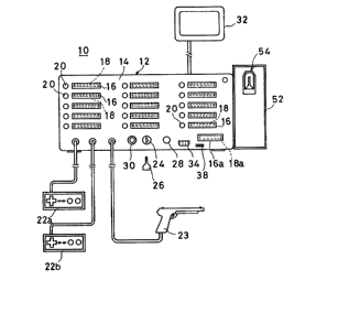
Figure 1 is an appearance view showing one
embodiment in accordance with the present invention. A
game software service system 10 comprises a cubic main unit
S 12, and a front panel 14 is formed in the front portion of
the main unit 12. A plurality of (15 in this embodiment)
slots 16 are formed in the front panel 14, and although not
illustrated a multi-pin connector connected to pins of a
game cartridge 18 is installed in the inner part of each of
these slots 16.
Accordingly, these slots 16 can load the game
cartridges 18 in an attachable/detachable manner by the
multi-pin connectors. Then, in the vicinity of each slot
a light emitting diode (LED) 20 is installed, which is for
displaying that the game cartridge 18 is loaded in the slot
16, or whether or not the loaded game cartridge 18 is being
utilized.
Controllers 22a and 22b which play the game and
are utilized to select the game cartridge 18 loaded in each
slot 16 and also a light gun 23 for playing shooting game
are connected to the front panel 14.
Further a key switch 24 for selecting whether the
game is to be abled or to be disabled is installed on the
front panel 14, and the key switch 24 is made operable by
2S inserting a key 26.~ Accordingly, in the case where such a
game software service system 10 is installed, for example,
in the guest room of a hotel or the like, the key 26 will
be lent out to the user at the front of the hotel in
exchange for the charge for utilization.
Also, on the front panel 14, a reset switch 28 and
a TV/game change-over switch 30 are installed in the
:~ vicinity of the key switch 24. The reset switch 28 is used
to reset the game when the user plays the game. The
TV/game change-over switch 30 is a switch for change-over
between reception of normal television broad casting by a
;B .
~ ,, .
"~ ..
... . .. . .
1284~;~5
TV receiver 32 utilized as a monitor and display of the
game images or CATV images utilizing the TV receiver 32.
Further an expansion connector 34 is installed on
the front panel 14, and the expansion connector 34 has
functions equivalent to those of the expansion connector of
the existing Family Computer (trademark) or Nintendo
Entertainment System (trademark) manufactured and sold by
the applicant of the present invention, being utilized, for
example, for connecting a joy stick controller.
Another slot 16a is installed in the main unit 12,
and a monitor memory pack 18a having a system program is
stored in the slot 16a. The memory pack 18a may be of the
same shape as those of the game cartridges 18 loaded in the
other slots 16, and performs control of the whole system,
for example, controls displays of the demonstration image,
the menu image or the like, selection of the game software,
connection to the CATV line, and charging money put in the
coin box.
A dip switch 38 is further installed in the main
unit 12. The dip switch 38 is constituted as eight bits,
and can be utilized for changing over the money charging
system, setting unit time of timer according to the unit
amount of money of coins to be put in, and so on.
As shown in Figure 2, a power supply unit 42 is
installed on a rear panel 40 of the game software service
system 10, and the power supply unit 42 is constituted so
a5 to be attachable to and detachable from the rear panel
40 and thus the main unit 12.
In the power supply unit 42, an AC input connector
42a for connecting an AC power supply and an AC output
connector 42b for supplying other equipment, for example,
the TV receiver 32 for monitoring (Figure 1) with power are
installed. Furthermore, an expansion I/O connector 43 is
installed on the rear panel 40. The expansion I/O
connector 43 is utilized as an input/output port when a
~, MODEM or the like is connected.
~ 1
', ;`"
,. . . .
- .
:
,.
...
1284~5
On the rear panel 40, further an output terminal
44 which can be connected to a video input terminal (not
illustrated~ of the monitor or the TV receiver 32 and an
audio output terminal 46 which can be connected to an audio
input terminal (not illustrated) of the TV receiver 32 are
installed. In the case where such a TV receiver 32 does
not have those video input terminal and audio input
terminal, a RF output terminal 48 is connected to an
antenna terminal thereof (not illustrated). Further, on
the rear panel 40, an antenna input terminal 50 for
connecting an antenna cable to the system 10 is installed.
F-connector plugs are utilized for these terminals 48 and
50, respectively.
Reverting to Figure 1, a coin box 52 which is one
of money charging systems is installed in this system 10,
and a coin inlet 54 for putting in coins is formed on the
coin box 52. Accordingly, the system of this embodiment
can be constituted also as a coin-timer controlling system
capable of playing the game for the time according to the
amount of money of the coins put in the coin box 52.
Figure 3 is a block diagram showing a
configuration of this embodiment. In reference to Figure
3A, the game software service system 10 comprises a
microprocessor or CPU 60. For this CPU 60, for example,
the integrated circuit "2A03" manufactured by Nintendo can
be utilized. A PPU (Picture Processing Unit) 62 is
connected to the CPU 60, and for this PPU 62, like the
Family Computer (trademark) or Nintendo Enter~ainment
System (trademark), the integrated circuit "2C02"
manufactured by Nintendo can be utilized. Details of the
CPU 60 and the PPU 62 are shown in U.S. Application Ser.
No. 14,150, now U.S. Patent No. 4,824,106. A clock of, for
example, 21.48 MHz is given to the CPU 60 and the PPU 62
from a common oscillator 64.
An eight-bit data bus 68 is connected to the data
port of the CPU 60 through a two-way buffer 66, and a 16-
~tl
, ~
lX84~ZS
bit bus 72 is connected to the address port through a one-
way buffer 70. Likewise, the data port of the PPU 62 is
connected to an eight-bit data bus 76 through a two-way
buffer 74, and the address port is connected to a six-bit
S address bus 80 through a one-way buffer 78. Furthermore,
an address latching circuit 79 is installed in the data
port of the PPU 62, and the address latching circuit 79
latches address data outputted in a time shared manner from
the data port of the PPU 62, giving the same to the one-way
buffer 78 as 14-bit address data along with six bits from
the address port of the PPU 62. The address data from the
CPU 60 outputted through the address bus 72 is given to an
address decoder 82. This system is constituted by the so-
called memory map system, and accordingly, the address
decoder 82 decodes a five-bit address from the CPU 60,
outputting required chip enable signals CEO - CE8,
respectively. Also, a system clock ~2 from the CPU 60 is
given to the address decoder 82, being given also to
another address decoder 84. Likewise, the address decoder
84 also outputs required chip enable signals CE9 - CEll
from four-bit address data.
In reference to Figure 3A and Figure 3B, a working
RAM 86 is installed in association with the CPU 60, and a
video RAM 88 is installed in association with the PPU 62.
The workinq RAM 86 is enabled by the chip enable signal CEl
from the address decoder 82, and is given the address data
from the CPU 60 through the address bus 72, also being
given the data from the CPU 60 through the data bus 68. To
the:video RAM 88, the data from the PPU 62 is given through
the data bus 76 of the PPU 62, and also the address data
from the PPU 62 is given through the address bus 80. The
most significant bit of the address bus 80 of the PPU 62 is
given as a chip enable signal of the video RAM 88 through
an inverter 90. This means that the video RAM 88 is
enabled when the most significant bit of the address bus 80
is "1".
.~ :?
, ' ': ^ .
':~
: ' .. ' : ' -
.: - '"
.:
. ~ : ,
1284~X5
In reference to Figure 3A and Figure 3B, the
controllers 22a and 22b connected to the main unit 12 are
both connected to a controller switch-over circuit 94
through I/0 interfaces 92a and 92b. The controller switch-
over circuit 94 is a circuit for switching to either of thecontrollers 22a and 22b to use it as a main controller, and
in the embodiment, the controller 22a or 22b used to select
the game cartridge 18 is set as such a main controller. In
addition, the I/O interfaces 92a and 92b for the
controllers 22a and 22b are enabled by chip enable signals
from a decoder built in the CPU 60, respectively. Also,
the controller switch-over circuit 94 is enabled by the
chip enable signal CE4 from the address decoder 82. Then,
operation signals or data from the controllers 22a and 22b
are stored in the working RAM 86 through the controller
switch-over circuit 94 and a reset controlling circuit 96
via a data bus 100, being utilizing for game control.
The reset switch 28 installed on the front panel
14 is connected to a reset controlling circuit 96. The
reset controlling circuit 96 is connected to the controller
switch-over circuit 94. When the key switch 24 is turned
on, when reset switches (not illustrated) of the
controllers 22a and 22b are depressed, or when a
presettable timer 98 expires, the reset controlling circuit
96 outputs a reset signal to the CPU 60 in response to any
signal thereof. Specifically, the reset controlling
circuit 96 includes a circuit for selecting any one of
various reset signals from the reset switch 28, the
controller switch-over circuit 94 and the presettable timer
98 as described later and a flag for deciding the reset
signal having come and storing it, and is enabled by the
chip enable signal CE3 from the address decoder 82.
The presettable timer 98 is utilized as a timer
for presetting the time during when the game can be played
according to the amount of money of the coins put in the
coin box 52, and for this purpose, the presettable timer 98
B
lZ84~5
is connected to a coin selector interface 102 connected to
the working RAM 86 and the coin box 52 by the eight-bit
data bus 100. The coin selector interface 102 gives the
kinds of the coins put in through the coin inlet 54 (Figure
1) and the total number of each kind of coins to the
working RAM 86 through the data bus 100.
The CPU 60 outputs an audio signal such as
necessary effect sound responding to the progress of the
game, and the audio signal is given to an AV-RF controller
104. A video signal from the PPU 62 is further given-to
the AV RF controller 104, and the AV RF controller 104
turns on or off the audio signal and the video signal given
in such a manner, giving them to a RF modulator 106. The
RF modulator 106 outputs composed of audio signal and video
signal from the AV-RF controller 104, for example, as a
television signal of the NTSC standard, that is, an RF
signal. However, the audio signal and the video signal can
be outputted separately as respective base band signals
from the RF modulator 106. The video signal from the RF
modulator 106 is outputted from the above-described video
output terminal 44 as shown in Figure 2, and the audio
signal is outputted from the audio output terminal 46.
Likewise, the RF signal from the RF modulator 106, that is,
the television signal is outputted from the RF output
terminal 48.
As shown in Figure 1, a plurality of slots 16 (16
810tS including a built-in slot 16a) are installed, and the
game cartridge 18 is loaded in each of the slots 16. A
plurality of game cartridges 18 and one monitor memory pack
18a loaded in such a manner constitutes one block by a
predetermined number (four in this embodiment), and in this
embodiment, since 16 slots 16 (16a) are formed, four blocks
BLK0 - BLK320 are formed. Each of the blocks BLK0 - BLK3
is composed of four banks BK0 - BK3, respectively. In
Figure 3C, only the block BLK0 is illustrated in detail on
behalf of other blocks since they are constituted in the
.D' ~.
.
. . .
:..-:
. ~ ..... ' .
'. ''
.. : .,: ,
.
1284~5
same manner. However, it is pointed out in advance that
the blocks BLKl - BLK3 are; constituted also in the same
manner.
The respective banks BK0 - BK3 of each of the
blocks BLK0 - BLK3 are connected in parallel so as to be
located in an overlapped manner in the same address space
when viewed from the CPU 60 and the PPU 62, but only the
bank (game cartridge 18) corresponding to one game software
selected by the menu mode is enabled selectively.
The program memory pack 18a loaded in one slot 16a
included in the block BLK0 is allocated as the bank BK0,
and the game cartridges 18 loaded in three slots 16 are
allocated as the banks BKl - BK3, and each of the game
cartridges, that is, the banks BKl - BK3 includes a program
memory and a character memory. The blocks BLK0 - BLK3 are
selected by a demultiplexer 108 for selecting the block,
and the program memory is selected by a demultiplexer llo
and the character memory is selected by a demultiplexer
112, respectively.
To be detailed, an eight-bit data is given to an
output port 114 from the CPU 60 through the data bus 68,
and the output port 114 outputs a four-bit data
representing the blocks BLK0 - BLK3 and the banks BK0 - BK3
in accordance with the eight-bit data. The demultiplexers
25 108-112 decode the four-bit data given from the output port
114 in such a manner, outputting signals for selecting any
one of the blocks BLK0 - BLK3 and any one of the banks BK0
- BK3. For example, the banks BK0 - BK3 of the block BLK0
are enabled by select signals from the demultiplexers 110
30 and 112.
A signal from the demultiplexer 108 for specifying
the block is given to a bus buffer 116 associated with the
respective blocks. The bus buffer 116 includes a two-way
buffer 118 for the proqram memory, a one-way buffer 120 for
address for the program memory, a two-way buffer 122 for
the character memory and a one-way buffer 124 for address
.
:
~ ... .
~. , .' ~ -' ~
. .
- -
.... : -
.. . . . ...
.~ .
1284~Z5
for the character memory. out of the four-bit select
- signal from the demultiplexer 108, two bits are given to
the bus buffer 116, and one bit thereof enables the two-way
buffer 118 and the other bit enables the two-way buffer
122, respectively.
In addition, the two-way buffer 118 for the
program memory is connected to the data bus 68 of the CPU
60, and the two-way buffer 122 for the character memory is
connected to the data bus of the PPU 62. Likewise, the
one-way buffers 120 and 124 for address are connected to
the address bus 72 of the CPU 60 and the address bus 80 of
the PPU 62, respectively.
An expansion box interface 126 is connected to the
expansion multi-pin connector 34 as shown in Figure 1, and
in this embodiment, a CATV interface 128 is installed to
enable coupling with a CATV system. The expansion box
interface 126 and the CATV interface 128 are enabled by the
chip enable signals CE10 and CEll from the address decoder
; 84, respectively.
Also, an expansion I/0 port 130 is connected to an
I/0 connector 42c installed on the rear panel 40, and the
expansion I/0 port 130 is enabled by the chip enable signal
CE8 from the address decoder 82.
Next, description is made on operation of this
embodiment based on Figure 4A through Figure 6 in reference
to Figure 1 through Figure 3.
~ Flow charts as shown in Figure 4A and Figure 4B
start every time a reset signal is given to the CPU 60 from
the reset controlling circuit 96. This means that the
reset controlling circuit 96 gives a reset signal to the
CPU 60 in response to turn-on of the key switch 24 (Figure
I) by the key 26, operation of the reset switch (not
illustrated) of the controller 22a or 22b, turn-on of the
~ reset switch 28 of the main unit, or reception of a time-
up signal from the presettable timer 98. Responsively, inthe first step Sl, the CPU 60 outputs a signal to the
.^ . .
,
.
... .. . . . . .
- ,~
-
1284~5
13
address decoder 82 and sets the chip enable signal CEl from
the address decoder 82 to "o", thereby disabling the reset
controlling circuit 96.
Accordingly, at this point, the reset signal from
the reset controlling circuit 96 is inhibited.
In the next step S3, the CPU 60 and the PPU 62 are
initialized. This means that registers, ports and so on
associated with the CPU 60 and PPU 62 are set to the
cleared state from the unfixed state.
In the next step S5, the CPU 60 determines the
kind of the triggered reset signal. The reset signals from
the controllers 22a and 22b, the reset switch 28 and the
presettable timer 98 are decided as the "Hot" reset, and
the reset signal by turning on the key switch 24 is decided
as the "Cold" reset. To decide the kind of signal in the
step S5, the reset controlling circuit 96 has only to
output a reset signal and a flag representing the kind of
that reset signal in accordance with the kind of the signal
by which the reset controlling circuit 96 is triggered.
When the "Cold" reset, that is, the reset by turn-
on of the key switch 24 is detected in the step S5r the CPU
60 disables the presettable timer 98 through the address
decoder 84 in the following step S7. This means that in
the step S7, the CPU 60 inhibits the reset from the
presettable timer 98.
Thereafter, in the step S9, the CPU 60 gives a
signal to the address decoder 82, sets the chip enable
signal CEl to "1", and enables the working RAM 86, and also
outputs "0" to the data bus 86 through the two-way buffer
66 to clear a predetermined area "OOOOH-lFFFH" of the
working RAM 86. Also, in the next step Sll, the CPU 60
initializes the associated registers and input/output
ports.
In the step S13, the PPU 62 enables the video RAM
88 by giving data to the address bus 80 through the one-way
`:
. . .
. ~ .
lZ84225
buffer 78, and clears the video RAM 88 by outputting "0" to
the data bus 76 through the two-way buffer 74.
In the step S15, the CPU 60 initializes each
memory. Then, in the step S17, the CPU 60 enables an area
that is part of the working RAM 86 and stores the control
codes, that is, an S-RAM control area. Specifically, the
CPU 60 sets the enable signal CEl to "1" through the
address decoder 82 and enables the working RAM 86, and also
outputs the address for that area to the address bus 72
through the one-way buffer 70. Thereby, the S-RAM control
area of the working RAM 86 is enabled.
In the following step Sl9, the CPU 60 transfers
the program stored in the monitor memory pack 18a (Figure
1), that is, the program of the bank BKO to another address
space. This means that since the banks BKO - BK15 as shown
in Figure 3 are all allocated to the same address space,
the control program cannot be left intact together with the
game cartridge 18 in the same address space, and therefore
the monitor memory pack 18a of the bank BKO is transmitted
to the S-RAM control area of the working RAM 86 enabled
previously.
In the step S21, the CPU 60 checks "Check-Sum"
according to the program transferred to the S-RAM control
area. This means that all data of the game cartridges of
the banks BKl BK15 are totalled and the totalled result is
checked, and thereby decision is made on whether the game
cartridges allocated to these banks BKl - BK15 are loaded
or removed or whether the game cartridges are authentic or
un~ust.
Specifically, the CPU 60 enables the output port
114 by setting the chip enable signal CE5 to "1" through
the address decoder 82, and also it selects sequentially
the game cartridges 18 loaded in the respective slots 16,
that is, the banks BKl - BK15 by sequentially setting
~35 numeric values from "0001" to "OFFF" through the two-way
buffer 66 and the data bus 68. Then, the program data and
~., .
.,
,.. .
,, , ,' ' : ' - -
.
1284~5
the character data from these banks BKl - BK15 are stored
in the working RAM 86 through the two-way buffer 118 and
the data bus 68, and the CPU 60 adds all data of the game
cartridges 18, that is, the banks BKl - BK15 by accessing
to that area of the working RAM 86. In this embodiment, by
executing the step S21, decision can be made on whether or
not a proper game cartridge is loaded in each of the slots
16 and the like.
Also, in the step S23, the game title of the game
cartridge 18 loaded in each slot is checked by "Check-Sum"
in the step S21. This means that if the game cartridge is
registered in advance, the title of the usable game is
known by the result of this "Check-Sum", and in the case of
a non-registered game cartridge, the title of the game can
be decided by checking the specific code in that game
cartridge.
Thereafter, in the step S25, the CPU 60 sets an
"Hot" start flag formed in a predetermined area of the
working RAM 86, entering an attraction mode. The
attraction mode is a mode wherein information on the hotel
is displayed and demonstration of the game contents set in
this system is performed in a repeated manner using the TV
receiver 32 (Figure 1).
On the other hand, if decision is made to be "Hot"
reset in the previous step S5, the steps S29 and S31 are
executed, and thereby the predetermined area of the working
RAM 86 is cleared and the video RAM 88 is cleared likewise
the previous steps S9 and S13.
In the step S33, the CPU 60 decides on whether the
"Hot" reset has come from the reset switch 28 on the front
panel 14 or from the presettable timer 98, or whether from
~ the controller 22a or 22b by checking the flag inputted
: from the reset controlling circuit 96. Then, if
determination is made to be the reset signal coming from
the reset switch 28 on the front panel 14, processing
proceeds intact to the attraction mode as shown in the
, ;,
~'~'' .
: .
1;;~84~5
16
previous step S27. This means that the CPU 60 selects the
bank BK0 of the block BLK0 and executes the program of the
monitor memory pack 18a without fail when it is given a
reset signal in a hardware fashion from the reset switch 28
or the presettable timer 98, and selects any one of banks
other than the bank BK0 of the block BLK0 and executes the
program of the corresponding cartridge 18 when the kind of
game software is selected by the controller 22a or 22b in
the menu mode as described later, and restarts execution of
the program with the leading address of the game cartridge
18 selected previously when the reset switch of the
controller 22a or 22b is operated.
When decision is made not to be the reset signal
from the reset switch 28 on the front panel 14, in the next
step S35, the CPU 60 checks the state or mode of the
controller 22a or 22b. This means that the controller 22a
or 22b is sometimes depressed during execution of the
normal game, and is utilized also to select the game
cartridge 18 loaded in each slot 16, and therefore in this
step S35, the CPU 60 decides the mode where in the
controller 22a or 22b has been operated, and determines the
corresponding program to be executed.
In the step S35, when decision is made that the
controllers 22a and 22b have been depressed in the reset
mode, in the next step S37, processing proceeds to the menu
mode for selecting the game cartridge.
In reverse, if the controller 22a or 22b has been
operated during play of the normal game, in the step S39,
the CPU 60 decides whether it has been operated during
demonstration of the game or during play of the game. This
can be decided easily by checking the flag set in the
working RAM 86. Then, where the reset signal from the
presettable timer 98 has been given during demonstration of
the game, processing proceeds to the previous step S27 and
the attraction mode is executed. Furthermore, where the
reset signal from the presettable timer 98 has been given
.
,
1284~5
during play of the game, in the next step S43, expiration
of the presettable timer 98 is displayed, and processing
proceeds to the step S27.
In reference to Figure 5, in the first step S101
of the attraction mode, the CPU 60 displays the attraction
mode. This means that in the step S101, information on the
hotel where this system is installed or the like is
displayed on the screen of the monitor or TV receiver 32.
This is executed by cooperation of the CPU 60 and the PPU
62. Specifically, like the Family Computer (trademark) or
Nintendo Entertainment System (trademark), based on the
data from the monitor memory pack 18a (Figure 1), the audio
signal is outputted from the CPU 60 and the video signal is
outputted from the PPU 62. These two signals are given to
the RF modulator 106 through the AV RF controller 104.
Then, the signal from the RF modulator 106 is given to the
monitor, that is, television receiver 32, and thereby such
a display of information can be performed.
Then, in the next step S103, the CPU 60 gives a
black screen display command signal to the PPU 62 to turn
off the screen of the monitor 32.
In the next step S105, likewise the step S15 in
Figure 4A, the CPU 60 enables the S-RAM control area of the
working RAM 86.
Then, in the next step S107, the CPU 60 checks the
next bank number, that is, the current game number by the
data from the game cartridge 18 given from the data bus 68.
In the next step S109, likewise the step S17 in Figure 4A,
the program of the monitor memory pack 18a is transferred
to the S-RAM control area of the working RAM 86.
Thereafter, in the steps Slll, S113, S115 and
S117, the CPU 60 sets respective flags or data in the S-RAM
control area. To be detailed, in the step Slll, the CPU 60
sets the next bank number checked in the previous step S107
in the SRM control area. In the step S113, the CPU 60
gives data to the S-RAM control area, and sets the
. .
1~84~5
18
controllers 22a and 22b to the reset mode in the reset
controlling circuit 96. In the step S115, the CPU 60 sets
the flag showing that the game is being demonstrated, that
is, the game demonstration flag in a predetermined region
of the S-RAM control area. Then, in the step S117, the CPU
60 presets time data in the presettable timer 98 according
to the amount of money of the coins put in the coin box 52,
and thereafter processing enters the demonstration mode of
the game. This means that processing enters the
demonstration mode of the game. This means that processing
jumps to the reset area of the game cartridge of the bank
number set in the previous step Slll in the state that
reset is applied by the program, and the game by that game
cartridge is started.
In reference to Figure 6, description is made on
the menu display mode. In the first step S201 of this
mode, a menu is displayed on the screen of the monitor 32
by cooperation of the CPU 60 and the PPU 62, and likewise
the previous step S107 (Figure 5), the next bank number,
that is, the current game number is checked.
The steps S203, S205 and S207 are the same as the
steps S103, S105 and S109 in Figure 5 respectively, and
here the duplicate description is omitted.
Thereafter, in the step S209, likewise the
previous step Sll, the number of the cartridge to be set
next, that is, the bank number is set in the S-RAM control
area of the working RAM 86. In the step S211, the CPU 60
sets the controllers 22a and 22b to the control mode, that
is, the program mode. In the step S213, the CPU 60 sets
the flag showing that the game is being played, that is,
the game play flag in a predetermined area of the working
RAM 86. Thereafter, in the step S215, a signal is given to
the reset controlling circuit 96, and the CPU 60 allows an
input of reset from the reset switch 28 on the front panel
14. Then, time of a length according to the amount of
money of the coins put in the coin box 52 is preset in the
~3
lX~4~Xs
19
presettable timer 98, and processing proceeds to the game
play mode.
- In addition, systems of charging money in this
system conceivably include three systems; a CATV system, a
key system and a coin system. In the CATV system the CPU
60 gives a signal to the address decoder 80, and enables
the CATV interface 128 by setting the chip enable signal
CEll to "1". Then, a CATV network installed in the hotel
or the like is coupled with this system 10. Then, the game
mode is set by operating the TV/game change-over switch 30.
Next, the monitor, that is, TV receiver 32 is set to a
proper unoccupied channel. In this state, a game
demonstration image or an operation procedure image is
displayed by the attraction mode as shown in the previous
Figure S. By operating an arbitrary key of the controller
22a or 22b, the first mode is performed, and by operating
a select button (not illustrated) installed in the
controller 22a or 22b in that state, the game cartridge
loaded in the slot 16, that is, the game program allocated
to any one of the banks BKl BKlS is selected. Then, the
start button of the controller 22a or 22b is depressed to
start the game. Money has only to be charged at this
point. Thereafter, on ending the game, setting is made to
the TV reception mode by operating the TV/game change-over
switch 30.
In the key system, the key 26 is lent out to the
user at the front of the hotel where this system 10 is
installed. In this case, a certain amount of money has
only to be charged at this point. Thereafter, change-over
is made to the game mode by operating the TV/game change-
over switch 30, and the monitor, that is, TV receiver 32 is
set to a proper unoccupied channel. Then, the
demonstration or the operation procedure is displayed, and
by inserting the key 26 lent out from the front into the
key switch 24 and turning it in that state, the game is
made playable. Then, likewise the previous CATV system, by
. , ' ~. .
.
lZ84~5
utilizing the controllers 22a and 22b, selection and start
of the game are performed, and after the game has ended,
the TV reception mode is set by operating the TV/game
change-over switch 30.
In the coin system, change-over is made to the
game mode by operating the TV/game change-over switch 30,
and the TV receiver 32 is set to an unoccupied channel. In
this state, the user puts in a certain amount of coins
through the coin inlet 54 of the coin box 52. Then, a game
time is set in the presettable timer 98 according to the
data of the amount of money from the coin selector
interface 102 connected to the coin box 52. Then, the game
cartridge is selected and the game is started by the
controller 22a or 22b. Then, when the time of a lenqth
according to the amount of money of the coins put in
elapses, the game is brought to an end by a time-up signal
from the presettable timer 98. Thereafter, setting is made
to the TV reception mode using the TV/game change-over
switch 30. In the case where the coin mode as described
above is utilized, it is considered also that the coin box
52 is constituted so as to be used in common as a coin
timer of the existing TV receiver provided in the room
of the hotel.
Furthermore, a remote control function can be
constituted also using this system. For example, by using
the CATV interface 128, calculation of charged money can be
performed in the working area of the CPU 60 or the power
supply of the system including the TV receiver 32 as a
monitor can be turned on or off through the CATV line of
the hotel or the like.
Also, by using the AC power line, for example
exchange of arbitrary game software data can be also
performed between the front and the room.
Record data of utilization of this system are
reserved in the working RAM 86 of this system, and are made
c~
.
1~84~5
accessible from the front, and thereby the amount of money
of the coins put in can be made sure.
In addition, in the above-described embodiment, to
facilitate exchange of the game software, the memory
cartridge 18 is loaded from the outside of the main unit
12, but it may be loaded in an attachable/detachable manner
in the main unit 12. Also, the menu is selected by the
controller 22a or 22b, but another select switch may be
installed.
Figure 7 is a block diagram showing portions
operated by coins which can be utilized for the above-
described embodiment.
As described above, the ~P 60 and the PPU 62
receive data from the respective ROMs of the game cartridge
18 connected selectively by the selector 116, perform
proper data processing, and give the audio signal and the
video signal to the interface 104, respectively.
The interface 104 includes a level shifter 136-for
shifting up or shifting down the signal level, preferably
the luminance level of the video signal in particular out
of the video signal and the audio signal to be given. The
level shifter 136 operates in response to an output from an
AND gate 138. A "near end" signal and a clock ~4 from the
coin box 52 are given to two inputs of AND gate 138.
2S AccordingIy, the level shifter 136 changes the luminance
level of the video signal to be given in response to the
period or the clock ~4 when the "near end" signal is given.
Then, the video signal and the audio signal
passing through the level shifter 136 are outputted from a
buffer circuit 140 through the video output terminal 44 and
the audio output terminal 46. Also, a signal is given to
the RF modulator 106 from the buffer circuit 140, and the
RF modulator 106 modulates the video signal and the audio
signal to be given into a high frequency signal or RF
signal such as a television signal of the NTSC standard.
The RF signal is outputted from the RF output terminal 48.
.
,.
;
.. . .
lX84~5
The ~P 60 gives a signal for directing any one to be
enabled of the game cartridge 18 to the above-described
selector 116, and gives a command signal for selecting the
repetition frequency of the reference clock used for time
counting in the coin box 52, that is, for selecting any one
of clocks ~ 3 having different frequencies to the coin
box 52. The coin box 52 outputs the above-described "near
end" signal and the clock ~4, and also outputs a timer-on
signal, giving them to the reset circuit 96.
10 ~ A monostable multivibrator 132 which is triggered
by the above-described timer-on signal given from the coin
box 52 is installed in the reset circuit 96. The
monostable multivibrator 132 is triggered, for example, by
the trailing edge of the timer-on signal to be given, being
a monostable multivibrator of so-called edge triggering
type. In the reset circuit 96, a reset signal generating
circuit 134 is~further installed which receives an output
of *he monostable multivibrator 132 and an operation signal
from the reset switch 28 (Figure 2) on the-front panel 14.
The reset signal generating circuit I34 outputs a reset
signal in response to an operation of the reset switch 28,
receives an output signal from the monostable multivibrator
132, generates a reset signal, and holds it. The reset
signal from the reset circuit 96, that is, the reset signal
generating circuit 134 is given to the reset input of the
P 60.
In addition, the controllers 22a and 22b are
connected to the ~P 60 through the controller I/0 92.
Then, the ~P 60 gives a select signal to the selector 116
in response to an operation of either of the controller 22a
and 22b, and the game can be played by operating the
contro}lers 22a and 22b.
Figure 11 shows a further detailed circuit
configuration of the coin box 52. A clock generator 142 is
installed in the coin box 52, and from the clock generator
142, for example, four kindslof clocks ~2, ~3 and ~4 having
,, :``,,
~ - . ' . ,
. . ., , ,..................... :
,
1284~XS
23
different repetition frequencies respectively are
outputted. Then, the clocks ~ 3 are given to a clock
selecting circuit 144, and as described above, the clock ~4
is given as one input of the AND gate 138 (Figure 7)
included in the interface 104. The clock selecting circuit
144 selects any one of the three clocks ~ 3 to be given
based on the si~nal from the ~P 60. Selection of the clock
in such a clock selecting circuit 144 can be changed by the
~P 60 in accordance with the selected game cartridge. This
means that in this video gaming machine, any one of three
kinds of clocks is used according to the kind of game
(degree of difficulty) to be played, and thereby three
kinds of unit times of timer can be selected.
The selected clock from the clock selecting
circuit 144 is given to a count input of a counter 148
through a two-input AND gate 146. The counter 148 is
constituted, for example, as a 10-bit counter, and can
count "0-1023". A carrier signal or count-up signal
(outputted when 1024 is counted) from the counter 148 is
inverted and given as another input of the above-described
AND gate 146. The same count-up output of the counter 148
is inverted by an inverter 150, being outputted as the
above-described timer-on signal. The coins (not
illustrated) put in through the coin inlet 54 are detected
by a coin detecting circuit 152, and a coin detection
signal from the coin detecting circuit 152 is given as a
reset signal of the above-described counter 148. A
comparator 154 is installed, and the most significant four
bits of the counted value of the counter 148 are given as
one of comparison inputs A of the comparator 154. A set
data from a data setter 156 including the afore-mentioned
- dip switch 34 (Figure 2) is given as the other comparison
input B of the comparator 154. The data set by the data
setter 156 is any one of values 0-1023 counted by the
3S counter 148, and data equivalent to a time a little shorter
than the timer time of play allowed by the unit amount of
~"
....
-..
- - -
128~X25
money of the coins put-in is set. Accordingly, a signal
from the comparator 154 is outputted as the "near end"
signal for notifying in advance that the game is brought to
an end after a lapse of the time according to the amount
S of money of the coins put in at that time.
Next, description is made on operation in such a
circuit configuration.
When a certain amount of money, for example, one
100-yen coin is put in through the coin inlet 54 of the
coin box 52, this is detected by the coin detecting circuit
152, and a coin detection signal as shown in Figure 8A is
outputted from the coin detecting circuit 152. In response
to the coin detection signal, the counter 148 is reset, and
accordingly, the count-up signal of the counter 148 becomes
the low level at that point. Accordingly, the timer-on
signal being the output of the inverter 150 rises to the
high level at that point as shown in Figure 8B. In
response to the rise of the timer-on signal, the ~P 60 is
enabled, and starts processing of game information along
w~th the PPU 62, and thereby the player can play the game
on the screen of the TV receiver 32 as previously
described.
on the other hand, attending on a selection of the
kind of game by the player, in response to a signal
outputted from the ~P 60, any one of the clocks ~ 3
given from the clock generator 142 is selected by the clock
selecting circuit 144, being given to the AND gate 146. At
this time, the carrier signal or count-up signal of the
counter 148 is the low levelJ and accordingly, a clock from
the clock selecting circuit 144 is given to the counter 148
starts to count.
In due time, the counted value of the counter 148
becomes larger than the data set by the data setter 156.
Then, as shown in Figure 8C, the "near end" signal of the
high level is outputted from the comparator 154 at that
point. For example, assuming that a "15-minute" play can
~,
-
.
.
~284~;~5
be performed by one "100-yen" coin, this "near end" signal
is outputted one minute before a lapse of 15 minutes, that
is, when 14 minutes have passed. However, it is needless
to say that such a specific time can be set arbitrarily and
differs greatly depending on the place and conditions of
installation of this video gaming machine.
As shown in Figure 7, the ~near end~ signal from
the coin box 52 is given to the input of the AND gate 138
included in the interface 104 along with the clock ~4 as
lo shown in Figure 8D. Accordingly, from the AND gate 138, as
shown in Figure 8E, a signal equivalent to the clock ~4 is
outputted while the "near end" signal is the high level,
and the signal is given to the level shifter 136 as a blink
signal. Accordingly, as shown in Figure 9, this level
shifter 136 shifts the luminance level of the video signal
to be given. This means that the level shifter 136 keeps
the luminance level of the normal game image signal when
the blink signal to be given is the low level, and reduces
the luminance level when the blink signal is the high
level, outputting the video signal wherein the luminance
level varies in synchronism with the blink signal, that is,
the clock ~4. This video signal is given to the buffer
circuit 140. Accordingly, on the screen of the TV receiver
32, so-called blinking is produced that the luminance of
display varies little by little in response to the change
in the luminance level. Consequently, the player can know
that the rest of the gaming time allowed by the coins put
in is short by watching the screen of the TV receiver 32.
Then, if the player does not put in additional
coins again, the counter counts "1024", and the count-up
siqnal becomes the high level. Accordingly, the timer-on
signal falls as shown in Figure 8B, and the monostable
multivibrator 132 included in the reset circuit 96 is
triggered. Accordingly, a pulse is outputted from the
monostable multivibrator 132, being given to the reset
signal generating circuit 134. Accordingly, as shown in
,
.
lZ84;~5
26
Figure 8F, from the reset signal generating circuit 134, a
reset signal is given to the ~P 60 simultaneously with a
count-up of the counter 148. Thereby, the ~P 60 is reset
and thereafter the game playing cannot be continued.
S In the case where the player puts in additional
coins in the coin box 52 through the coin inlet 54 when
such a blink signal is outputted and blinking is performed
on the screen of the TV receiver 32, as shown in Figure
lOA, the coin detection signal is obtained again from the
coin detecting circuit 152. Consequently, the count-up
signal of the counter 148 is forced to become the low level
again at that point, and the timer-on signal from the
inverter 150 keeps the high level intact. Accordingly, the
monostable multivibrator 132 included in the reset circuit
96 is not triggered, and the reset signal of the ~P 60 is
not outputted from the reset circuit 96.
On the other hand, when an additional coin put-in
signal is obtained, the counter 148 is reset again, and
accordingly, the count-up signal is set to the low level.
Accordingly, the clock given from the clock selecting
circuit 144 continues to be given to the counter 148 intact
through the AND gate 146. Since the counter 148 has been
reset by the previous additional coin put-in detection
; signal from the coin detecting circuit 152, it starts to
count again from "0", continuing the operation described
previously in reference to Figure 8A through Figure 8F.
Then, after blinking has been produced, if no coin is put
in, the ~P 60 is reset intact, and the game playing after
that cannot be continued.
When additional coins put in are detected by the
coin detecting circuit 152, as shown in Figure lOC, the
"near end" signal falls to the low level at that point.
Consequently, thereafter the clock ~4 is not given to the
level shifter 136 from the AND gate 138 (Figure 7), and the
shifting operation of the luminance level by the level
shifter 136 is stopped. This means that in response to an
B
`.
.;
.
" ~84~5
additional put-in of coils, blinking on the screen of the
TV receiver 32 is stopped.
In the above-described embodiment in Figure 11,
even if coins are put in continuously before game playing
is started, they are not counted, and therefore virtually
continuous put-in is not accepted. Then, another
embodiment as shown in Figure 12 is proposed. In the
embodiment in Figure 12, the continuous put-in of coins
before starting playing the game is accepted.
In Figure 12, portions the same as or similar to
those in Figure 11 are designated by the same or similar
reference symbols, and thereby the duplicate description is
omitted.
In the embodiment in Figure 12, the two-input AND
gate 146 (Figure 11) receiving the clock from the-clock
selecting circuit 144 is changed to a three-input AND gate
146'. Then, the output signal from the coin detecting
circuit 152 is given as one of inputs of an OR gate 158.
To the other input of the OR gate 158, the count-up signal
from the counter 148 is given, and the output of the OR
gate 158 is given as a count input of an up-down (U/D)
counter 160. As an U/D input for directing either of
count-up and count-down in the U/D counter 160, a count-up
signal of the counter 148 is given intact. Then, the U/D
counter 160 counts down according to a signal or pulse from
the OR gate 158 when the U/D input to be given is the high
level. In reverse, the U/D counter 160 is put in the
count-up mode when the U/D input is the low level. The U/D
counter 160 is constituted, for example, as a four-bit
counter, and all four-bit outputs from the U/D counter 160
are given to a four-input OR gate 162. Accordingly, the
; high level signal is outputted from the OR gate 162 only
when the counted value of the U/D counter 160 is not "o".
An output of the OR gate 162 is given as a residual input
of the above-described AND gate 146'. Accordingly, the
counter 148 can receive the clock from the clock selecting
~^ ~
~ 1. .
. . .
' ' ~
1284~5
28
circuit 144 as a count input thereof through the AND gate
146' when the residual number of coins put-in is other than
"O" .
The four-bit outputs of the U/D counter 160 are
also given as respective inputs of a four-input AND gate
164. This means that only the least significant bit of the
U/D counter 160 is kept intact and the most significant
three bits are inverted, becoming respective inputs of the
AND gate 164. Accordingly, a high level signal is
outputted from the AND gate 164 only when the counted value
of the U/D counter 160 is "1".
Then, an output of the AND gate 164 is given as an
input of a two-input AND gate 166 along with the above-
described inverter 150. An output of the AND gate 166 is
given as the enable signal CE of the comparator 154.
Accordingly, the comparator 154 is enabled only when the
timer-on signal is the high level and the counted value of
the U/D counter 160 is "1", that is, only when the residual
number of coins put in becomes 1.
Description is made on the operation in the case
wh-re coins are put in continuously. When coins are put
in, one pulse is outputted from the coin detecting circuit
152 every time a coin is put in. The coin detecting signal
from the coin detecting circuit 152 is given to the count
input of the U/D counter 160 through the OR gate 158. At
this time, the counter 148 is reset by the coin put-in
signal, and therefore the count-up signal thereof is the
low level, and a low-level signal is given to the U/D input
of the U/D counter 160, and accordingly, the U/D counter
160 is put in the count-up mode. Consequently, when one
coin detection signal is given, the U/D counter 160 is
; incremented by "1", and resultingly the U/D counter 160
counts the number of the coins put in through the coin
inlet 54.
When the U/D counter 160 counts the number of the
coins put in, the output of the OR gate ~62 becomes the
'
.~ ~
1284~5
high level at this point, and thereby the AND gate 146' is
enabled, and the clock from the clock selecting circuit 144
is given as a count input of the counter 148. Thereby, the
counter 148 starts to count. When the U/D counter 160
counts "2" or more, the output of the AND gate 164 is low,
and accordingly at this time the comparator 154 is disabled
by the output of the AND gate 166. This means that even if
the timer-on signal from the inverter 150 is the high
level, the counted value of the U/D counter 160 becomes "2"
or more and the output of the AND gate 164 becomes the low
level, and therefore, the output of the AND gate 166
becomes the low level and the comparator 154 is not
enabled.~
on the other hand, since the counted value of the
U/D counter 160 is not "O", thereafter a high level signal
is outputted from the OR gate 162. Accordingly, the clock
from the clock selecting circuit 144 is given to the count
input of the counter 148 through the AND gate 146'. Then,
when a time equivalent to one coin put in elapses, that is,
when the counter 148 counts "1024", the counter 148~outputs
a count-up signal of the high level, and thereby the U/D
counter 160 is put in the count-down mode, and in response
to that signal, the U/D counter 160 counts "-1". This
means that the U/D counter 160 is decremented by "1" from
the number of the coins put in counted initially every time
the time equivalent to one coin elapses.
~ When the residual number of coins becomes "1", the
four-bit inputs to the AND gate 164 given from the U/D
counter 160 become all "1", and accordingly the comparator
154 is enabled at that point.
Thereafter, attending on the progress of count by
the counter 148, operations like ones as described early in
Figure 8A through Figure 8F or Fiqure lOA through Figure
lOF are performed. Thus, the player can enjoy the game for
a time according to the number of the coins put in before
starting playing the game. This means that the U/D counter
.:~
1284~25
160 counts the number of coins continuously put in
initially, and when the counted value is counted down to
~ , the comparator 154 is enabled for the first time at
that point, and therefore till then the "near end" signal
is not outputted even if the counted value of the counter
148 exceeds the value set by the data setter 156. For that
reason, during that period of time, no blinking is produced
on the screen of the TV receiver 32, and the player can
enjoy the game.
Although the present invention has been described
and illustrated in detail, it is clearly understood that
the same is by way of illustration and example only and is
not to be taken by way of limitation, the spirit and scope
of the pre8ent invention being limited only by the terms of
the appended claims.
,
~, .
~,
:, :
;; ,
::
: :
,
:
~B
. . ,
.
. ... - . .