Note: Descriptions are shown in the official language in which they were submitted.
3~
HIGH ORDER DIGITAL PHASE-LOCKED LOOP SYSTEM
BACRGROUND OF THE INVENTION
1. Field of the Invention
The present invention relates to phase-locked
loop systems and more particularly to digital
phase-locked loop systems. Phase-locked loops are
employed to generate a clock signal which is frequency
and/or phase referenced to an external input signal,
Phase-locked loop systems are used in many fields of
communications, and are also employed in computer
applications for data synchroniæation from peripheral
sources. The present invention is particularly directed
to the use of phase-locked loops for data separation in
disk drive systems when reading data informatio~ which
is interspersed with clock information.
:
- -- 2 --
BRIEF DESCRIPTION OF THE DRA~INGS
~ he invention will be described with reference to
the accompanying drawings, wherein:
FIG~RE 1 is a block diagram of a typical disk
drive/CPU system
FIGURES 2A-D are waveforms illustrating MFM
encoded signals;
FIGURES 3A-E are waveforms illustrating MFM
decoding;
FIGURE 4 is a block diagram of a phase-locked
loop (~LL) system to recover the clock and generate the
window or data separation;
FIGURE 5 is a block diagram of a PLL circuit
arrangement;
FIGU~E 6 is a block diagram of a digital PLL
arrangement;
FIGURES 7A-C are waveforms of 15-, 16- and 17-
state windows of the shift register of FIGURE 6;
FIGUR~ 8 is an expanded waveform diagram
illustrating the relation between a data stream and
window signals;.
FIGURE 9 is a block diagram of the present
~nvention;
FIGURES lOA-D are diagrams of the sample clock
and various windows employed in the present invention;
FIGURES llA and 11~ form a state diagram of the
digital controlled oscillator of the present invention
illustrating various preset operating frequencies;
FIGURES 12A and 12B form a flow chart for the
frequency tracking and correction state machine;
FIGURES 13A-C are state diagrams for ~he
transient response and phase correction state machine of
the invention, illustrating phase corre~tions applied to .
three different windows used to generate preset
frequencie~;
FIGURE 14 is a graph illustrating transition
pulse distribution within windows for random data; and
FI~URE 15 is a graph illustrating transition
pulse distribution for signals of ~pecific data content
typically encountered in a disk drive system~
- 2a -
Figure 1 illustrates a typical computing system
in which data is transmitted between a memory disk
system 10 and a central processing unit ~PU) 12. A
disk controller 14 is responsible for executing CPU
initiated commands to the disk drive electronicsJ This
includes writing properly formatted serial data to the
disk and accurately recovering data from the disk. The
computing system also typically includes an internal
memory 16 and a direct memory access (DMA) control 18.
Data written onto a disk consists of logic ones
and zeros which are written at a particular data, or bit
cell, rate. ~n order to accurately read the data from
the disk, the data rate of the signal being read mu~t be
known. This is facilitated by encoding the data which
15 is written onto the disk so that the signals include
.
J~
- 3 -
clock information as well as data information. The
embedded clock information is then employed to determine
the data rate when signals from the disk are being read.
Data is most commonly encoded on a disk in
modified frequency modulation (MFM) format~ MFM is a
digital signal, derived from the original
non-return to-zero (NRZ) data stream and a synchronous
clock signal. The rules of MFM encoding are that each
NRz logic one causes a transition in the MFM signal at
the center of the bit cell, and if an NR2 lo~ic zero
follows a logic one, the state of the MFM signal does
not change. If a logic ~ero ~ollows another logic zero,
there is an MFM transition at the boundary between the
two bit cells. An example of MFM coding is shown in
Figure 2. The NRZ data shown in Figure 2A is comprised
of a series of ones and zeros, each occupying a bit
cell. A clock signal indicated in Figure 2B defines the
bit cells~ The MFM signal shown in Figure 2C may be
generated from the NRZ data and clock signals by
exclusive-oring the data and clock to ~orm a phase
encoded signal, and then dividing the number of
transitions by two with a toggle flip-flop. It is only
the MFM transitions, not thei~ senses, that are
essential to decoding~ Typically, disk read electronics
are employed so that the signal recovered from a disk is
in the form of a narrow pulse for each MFM transition,
as shown in Figure 2D.
NRZ data may be recovered from MFM transitions as
shown in Figure 3. A window signal W, which i~ a
delayed clock C, is generated and used to distinguish
cen~er-of-bit-cell (data) from bound~ry-of-bit-cell
tclock) pulses. Each transition pulse T that occurs
during the window latches a window extension signal E
until the positive clock transition at the end of the
bit cell. When E is high at the end of the window
(negative transition of W) the NRZ data ~s a logic one;
when E is low at that time, the NRZ data is a logic
zero.
-- 4 --
Ideally, the clock rate of data read from the
disk is a known f ixed value. Due to various factors,
however, such is not the case~ and the clock rate of the
data must be determined by looking at the data itself
and generating the clock and window signals a~ the
appropriate frequency to track the data. The clock
signal is recovered from the MFM data using a
phase-locked loop driven by the transition pulses. The
function of the phase-locked loop is to provide clock
signals which are equal to the clock rate of the data
being read. Although the clock rate has a known ideal
value, the actual clock rate of the data will vary from
the ideal due to several factors. These factors include
variations in the speed that the data track moves past
the read head of the disk driver ;ncluding both
long-term and short-term disk speed variations, examples
of which are eccentricity and warping of the circular
data tracks. The purpose of the phase-locked loop is to
generate clock si~nals which follow such data rate
variations.
In addition to variations in the actual'data
rate, the timing of MFM pulses read from a disk deviate
' from the ideal due to high frequency noise at the read
head from external sources and adjacent tracks and noise
in the read electronics, and due to l'peak shift"~ i.e.,
a shi~ting of bit position due to the magnetic field of
adjacent bits of opposite polarity. The noise and peak
shift results in random bit jitter (movement of
transition pulses from their ideal positions) which is
unrelated to variations in the data rate. Since the
clock is recovered by reading the MFM pulses, the bit
jitter can adversely affect the recovery of the clock
signals.
~' . .
-- 5 -
2. Description of the Prior Art
To recover the original NRZ data and clock, a
phase-locked loop (~igure 4), driven by the transition
pulses, reconstruc~s the clock signal, and the recovered
clock and transition pulses are then decoded to give NRZ
data. Typically, the clock signals are delayed a
quarter of the clock period, and the delayed signal is
used as a window to distinguish transitions occurring
near the center of a bit cell from those occurring near
the edge of each bit cell~ Since only MFM transitions
are available, the clock and data regions of the window
signal (Figure 8~ cannot be uniquely identified with
respect to the data stream~ In practice MFM decoding is
done using both signals as windows and the detection of
a unique code is employed to determine which is the
correct decoded MFM signal.
Ideally, each transition will occur precisely in
the mi-ddle of the window signal. This will not always
be the case~ however, because of low frequency data rate
variations which are not precisely tracked by the
phase-locked loop and because of high frequency bit
jitter. If the transition moves outside of the limits
of the window, a read error will result. In order to
accurately track the data rate of the MFM data
transitions, the shift in the position of the
transitions as a result of bit jitter should be ignored,
whereas the shift in positions of the transitions as a
result of change in the frequency of the data should be
used to correct the frequency of the recovered clock and
resultant window.
The most common prior art systems employ an
analog phase-locked loop which incorporates low pass
filtering in order to eliminate the effects of bit
jit~er on the generation of the recovered clock. Such a
system is illustrated in Figure 5. A voltage controlled
oscillator (VCO) 20 is employed to generate the clock
sign~ls~ The output of the VCO is applied to a phase
detector 22, where its phase is compared to the phase of
the input signal (transition pulses~. The output of the
.
.
_ - 6 -
phase detector 22 is a signal with low frequency
components proportional to the phase error and hiqh
frequency components resulting from bit jitter. This
signal i5 applied to a low pass filter and amplifier 24
which atte~uates ~he high frequency components resulting
from bit jitter. The output of the filter ~nd amplifier
is a control voltage which is applied to the VCO 20 to
control its output frequency.
Although the analog phase-locked loop circuit of
Figure 5 generally has good-performance, it has several
disadvantages~ Such analog circuits are difficult to
design and build and require a large amount of circuit
board space. Additionally~ they require adjustments to
properly align the circuits in the system, i.e., to
adjust the VCO freguency and gains and currents of
various components. These adjustments are expensive in
terms of production costs since they result in lower
throughput and require technician overhead during
controller board manufacturing.
Digital phase-locked loop systems have been
designed in the past. A typical system is illustrated
in Figure 6. In such systems, a variable multiple state
component such as a counter or shift register 30
performs a function analogous to the VCO o~ the analog
phase-locked loop. The shift register is driven by a
sample clock 32. The carry output of the shift register
provides an ou~put signal of variable freguency which is
used to toggle the recovered clock window signal. The
output frequency of the shift register is varied by
adding or subtracting states, as illustrated in
Figure 7. For example, the shift register 30 may have
sixteen nominal states, as illustrated in Figure 7B. In
order to reduce the frequency of the window signal, one
state is added, as illustrated in Figure iC, and in
order to increase the frequency of the window signal,
one state is subtracted, as illustrated in Figure 7A~
A phase detector 34 is implemented with a
microprocessor or logic array and determines when the
_L~ i6
- 7 -
transition pulses arrive with respec~ to the states of
the shift register. The logic array incorporates an
algorithm to determine frequency corrections as a
function oE ~he determination of the state of occurrence
of the transition pulses. If a transition pulse does
not arrive in the correct state, the phase de~ec~r
provides an error signal on line 36 to alter the number
of states, and thus the output frequency, of the shift
register 30. Some prior art systems make only
instantaneous corrections in the number of states per
windQw as a function of the arrival of a transition
pulse in that particular windo~. Other systems make
both instantaneous corrections to a window based upon
the occurrence of a transition pulse in that particular
window as well as making long-term corrections based
upon the occurrence of transition pulses with respect to
previous windows.
The primary disadvantage of prior digital
phase-locked loops is that they are first order, i.e.,
they do not incorporate the concept of a filter. As a
resultr bit jitter adversely affects the operation of
the phase-loc~ed loop. ~his is to be contrasted with
higher order analog phase-locked loop systems in which
the bit jitter is filtered out and does not affect the
frequency tracking operation of the system. Since they
are only first order, prior art digital phase-locked
loops used for disk data separators have very low
performance, i.e., high data recovery error rates.
A more complex digital phase-locked loop system
is shown in U.S. Patent No. 4,357,707 to Delury. In the
system disclosed in this patent, adjustments in the
length of each window are made in accordance with the
arrival location of the current data pulse and
immediately preceding data pulse. These adjustments are
provided to correct the phase of the generated window
signal with respect to the incoming data. In addition,
adiustments are made to the nominal frequency of the
window signal in order to track frequency variations in
the data. Frequency changes are made when two
.
,
-- 8
consecutive data pulses arrive in a predetermined error
region. Although this system provides advantages over
simpler digital phase-loc~ed loop systems, its
performance still falls short of analog phase-locked
loop systems.
,
.
.
': :, ~ :
~3Æ~
g
SUMMARY OF I~HE I~ENTION
.
The present invention is directed to a digital
phase-locked loop system which achieves true second
order and higher performance. When implemented as part
o~ a disk data separator, the system operates to
effectively ignore bit jitter and track true frequency
variations in the data stream. In the present
embodiment of the invention, phase detection and error
amplification is provided by programmed state machines
which drive a digital controlled oscillator including a
variable state shift register to change the frequency of
the shift register output if appropriate. Filter
operation is provided by latching state machine output
" terms and feeding them back at la~er clock times. By
providing a system in which shifts in the occurrence of
transi~ion pulses due to bit jitter are ignored in
generating the window signal, very accurate data
separation is achieved, i.e~, read errors are minimized.
The digital controlled oscilla~or is alterable to
provide one of a plurality of preset output frequencies.
This is accomplished by controlling the number of states
in the shift register for each window si~nal. Frequency
and phase tracking is accomplished by monitoring the
arrival of each data pulse with respect to its
corresponding window and making changes in the length of
an individual window and/or the preset frequency. In
order to ensure that ali frequency changes are being
made in the proper direction, they are not made until
the position of at least three consecutive data pulses
with respect to their corresponding windows indicate
that a change in frequency should be made.
Instantaneous corrections to the length of an individual
window are made both as a function of khe position of a
data pulse occurring within that window and as a
function of the position of one or more previous data
pulses. These instantaneous changes serve ~o correct
large phase errors and to correct phase errors resulting
rom delays in making frequency alterations. The
operation of the system is completely symmetrical to
ensure linear filter operation.
--10--
DESCRIPTION ~r 5HE ~R~r~RREn Er3oD~M3N~
The following description is of the best
presently contemplated mode of carrying out the
invention. This description is for the purpose of
illustra~ing the general principles of the invention and
should not be taken in a limiting sense. The scope of
the invention is best determined by the appended claims.
Referring to Figure 8, a sample data stream of
transition pulses representing a data pattern 11001 is
illustrated. Transition pulses 40, 42 and 44 occur in
the middle of their respective bit cells, while
transition pulse 45 occurs at the edge of its bit cell.
The function of the phase-locked loop of the digital
data separator i8 to generate a window signal 48 which
enables center of bit cell transition pulses to be
discriminated from edge of bit cell transition pulses.
In an ideal system, each center of bit cell transition
pulse will occur in the center of a window. However,
the pulses may fall to either side of center as
illustrated by arrows 50 and 52 as a result of low
frequency data rate variations or high frequency bit
jitter. The purpose of the present invention is to
provide a data separator having a digital phase-locked
loop which will alter the frequency and phase of the
~5 window signal in order to track low freguency variations
of the data stream but will ignore the effects of high
frequency bit jitter on the data stream. By accurately
tracking low frequency variations, tolerance to bit
jitter will be increased, i.e., the transition pulses
will fall within the windows despite a relatively large
amount of bit jitter.
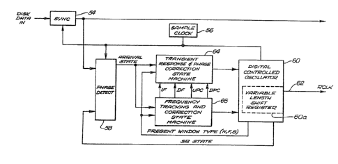
Figure 9 is a functional block diagram of the
digital phase-locked loop of the present invention. The
system includes three state machines, i. e., sequential
logic systems whose outputs depend upon previous and
present inputs, and their connections as shown are
functional representations. The input to the
phase-locked loop portion of the data separator directly
from the disk drive contains both MFM clock and data
information. The clock is recovered from the input
signal to provide a window signal for separation to
determine whether a transition pulse falls in a data
region or in a clock region. The separator then denotes
the position of the transition pulse with respect to the
window and adjusts the window according to a specific
algorithm. The goal of the algorithm is to keep the
pulses close to the center of the window as much as
possible (i~e., zero phase error) to allow maximum
tolerance to bit jitter. If the transition pulses are
always placed in the center of the window, then the
recovered clock will run at a fixed rate. However, if
the pulses come too soon, then the recovered clock will
be adjusted to run faster. Conversely, i the pulses
come too slow, the recovered clock will be adjusted to
run slower.
The primary components of the phase-locked loop
system of the present invention are a phase detector 58,
a digital controlled oscillator 60 which is comprised of
a variable length shift register 60a having plural
segments or "states" and a finite state machine, a
transient response and phase correction state machine 64
(hereinafter "phase correction state machinen) and a
frequency tracking and correction state machine 66
thereinafter "frequency correction state machine"). The
digital controlled oscillator 60 provides a recovered
clock, or RCLR, signal on line 62 which is comprised of
alternating windows of high and low level. This siqnal
is used in a manner known in the art to separate data
from clock signals in the original data stream from the
disk drive.
A single "one" i~ circulated through the
shift register and toggles the output signal on line
62 when i~ reaches the final state of the shift
registerr The phase of the oscillator is compared to
the data input signal by the phase detector 58. The
state machines 64 and 66 cause corrections to be made in
both the running frequency and phase of the output of
the oscillator based upon the detected phase error.
-12-
The transition pulses from a disk drive are
applied ~o a sync logic 54 comprised of an asynchrono~s
to synchronous detector which synchronizes the
transition pulses with pulses from a sample clock 56.
Each synchronized transition pulse from ~he logic 54 has
a pulse width of one sample clock pulse. In the present
embodimen~ of the invention, the digital data separator
is used in conjunction with a floppy disk system, and
the nominal bit cell rate is 250kHz. The sample clock
lo 56 is a 32x clock t32 times the bit cell rate), i.e.,
8MHz. A 500kHz (16 m~z sample clock) CMOS system has
also been developed~ The synchronized output is applied
to the phase detector 58 and compared to the shift
register states to determine the relative phase between
a transition pulse and the output of the oscillator 60.
In the present embodiment of the invention, the phase
detector is implemented in discrete logic. However, the
phase detection function could alternatively be
implemented in software.
The phase detector 58 provides a phase error
signal indicating the arrival state of a transition
pulse to the phase correction state machine 64 and the
frequency correction state machine 66. Based upon the
detected state of arrival, i.e, the state in which the
"one" circulating in the shift register was in when a
transition pulse arrived, the state machines 64 and 66
determine what corrections if any are necessary for the
digital controlled oscillator 60. The oscillator is
controllable to run at any one of a plurality of preset
steady state frequencies, and the frequency correction
state machine ~6 operates to determine if a change in
the preset frequency is required. The phase correction
state machine determines if instantaneous phase
corrections are necessary, io e., if one or more states
or an individual window must be added or subtrac~ed
independent of any changes in the preset frequency.
The operation of the system of Figure 9 to
achieve frequency tracking will be described with
reference to Figure 10. The 32x sample clock is shown
~13-
in Figure lOD. The digital controlled oscillator 60
controls the shift register to run at one of thirteen
different time-averaged frequencies, with each frequency
being achieved by combining windows of fifteen, sixteen
and seventeen shift register state duration, illustrated
in Fiqures- lOA, B and C, respectively. The nominal
frequency of the RCLR signal is 250k~æ (the same as the
nominal bit cell rate) and is achieved by repeatedly
generating "nominal" windows of sixteen state length.
The present embodiment of the invention is designed to
track frequency variations of up to * 6~ from the
nominal bit cell rate. Alterations in ~he time-averaged
frequency output of the shift register are achieved in
1~ increments. In order to increase the frequency by
6~, the shift register length is altered so that only
"fast" windows of fifteen state leng~h are employed.
Similarly, when a 6% reduction in frequency is required
the shift register is controlled so that only "slow"
windows of seventeen state length are employed~ The
fast and slow windows are shown in Figures lOA and lOC,
respectively. For frequencies other than the nominal
frequency, 6~ fast and 6% slow frequencies, two
different window types are combined to achieve the
desired time-averaged f requency~ The combinations of
fast, nominal and slow windows to achieve the various
output frequencies are shown in Table I as follows:
-14-
T~BLE I
Frequency Re~etitive Sequence of Windows
Nominal (o%): nominal
1% fast: fast-nominal-no~inal-nominal-nominal-
nominal
2% fas~: fast-nominal-nominal
3~ fast: fast-nominal
4% fast: fast-nominal-fast
s% fast: fast-nominal-fas~-fast-fast-fast
6~ fast: fast
1~ slow: slow-nominal-nominal-nominal-nominal-
nominal
2% slow: slow-nominal-nominal
3~ slow: slow-nominal
4~ slow: slow-nominal-slow
5~ slow: slow-nominal-slow-slow-slow-slow
. 6~ slows 810w
By repeating the se~uences of windows outlined above,
control of the time-averaged frequency can be achieved
in 1~ increments even though each individual window can
only be changed in 6~ increments ~one state out o~
sixteen). It should be noted that the +6% variation and
1% increments are arbitrary and that greater variation
and finer increments could be employed, albeit at the
expense of additional hardwareO The.chosen embodiment
provides a sati~factory balance of performance and
complexity.
Frequency tracking is achieved ~y the combination
of altering the set frequency of the digital controlled
oscillator and by making instantaneous changes in the
length of an individual window regardless of the set
frequency. The combination of frequ~ncy variation and
instantaneous changes provides a system having a second
order filter ~unction and which i3 slightly und2rdamped
to provide fast response with minimal ringingl
t~
-15-
Changes in the set frequency of the oscillator
are initiated in the response to either of two different
conditions. ~s shown in Figure 10~ each window is
divided into a "up" region including all states to the
left of the center of the window and a ~'down" region
including all states to the right of the center of the
window. Since a nominal window includes sixteen states,
its center is defined to include two states so that the
up region and down region are symmetrical. This is
important since symmetrical operation is necessary to
achieve linear optimization, i.e., the closest fit to
true linear operation in which filter gain changes
linearly from the center of a window to the edge of a
window
The frequency correction state machine 66
monitors the occurrence of transition pulses to
determine whether they occur in the up region, central
re~ion or down region. The occurrence of a single
transition pulse in an up region or down region is not
necessarily indicative of a frequency error, since the
pulse may be off center due to bit jitter. ~he
occurrence of two consecutive pulses in the up region or
two consecutive pulses in the down region is a better
indication that the error in positioning is due to
2s frequency error rather than bit jitter. However, even
two consecutive pulses provides only an approximately
50% probability that a frequency error exists in the
direction indicated. This is because errors due to bit
jitter will have a generally Gaussian distribution, as
indicated in Figure 14 (with small humps to either side
of middle due to peak shift), and the occurrence of two
consecutive pulses to either side of the middle of a
window may well be as a result of bit jitter as opposed
to frequency errors.
In the present invention, the occurrence of
transition pulses is monitored and the set frequency of
the oscillator i~ not changed until three consecutive
transition pulses occur in an up region or three
consecutive transition pulses occur in a down region.
By waiting un~il three consecutive pulses occur in a
-16-
particular region, the probability that there is an
actual frequency error in the direction indicated is
greatly increased. The primary drawback in waiting for
three consecutive pulses is that if there is indeed a
frequency error, the response is relatively slow and a
large phase drift may result before the frequency can be
corrected. In order to compensate for this lagging
operation, one-time phase corrections are made to
individual windows to shift the transition pulses back
toward the center of the window~ If two consecutive
transition pulses are detected in ~he up region or two
consecutive transition pulses are detec~ed in the down
region, a phase correction is made to the length of the
individual window in which the second pulse arrived.
The correction in all uses is either the addition or
subtraction of one state in the window. A similar phase
correction of one state is made upon the detection of
three consecutive transition pulses in the up region or
three consecutive transition pulses in the down region
(in addition to the frequency correction which i5 made
in that event~. Not only do khese phase corrections to
the length of an individual window serve to shift the
phase of the recovered clock signal to compensate for
drift due to lagging frequency correction, it also
serves to further increase the probability that any
changes in the set frequency will be in the proper
direction since subsequent transition pulses will also
be phase shifted toward the center of the window. In
effect, the phase correc~ion slows the slew rate of the
frequency correction function.
The frequency and phase corrections provided as
discussed above are extremely effective in tracking
actual frequency variations. However, filtering errors
remain due to the fact that the bit jitter in an actual
system with certain commonly encountered data patterns
is not equally distributed as illustrated in Figure 14.
Instead, there is a pattern dependency, i.e., in an
actual system some of the data patterns encountered are
such that the bit ji~ter will be nonsymmetrically
-17-
di~tributed with respect to the center of the window, as
illustrated in Figure 15. As a result, some frequency
drifts may not be accurately detected by the monitoring
of the up region and down region. In order to
compensate for this, additional filtering is
accomplished by monitoring edge regions at the outside
edges of each window. These edge regions are indicated
in Figure 10. Af~er each chan~e in frequency, the total
number of transition pulses occurring in either edge
region (whether or not they are consecutive) is
monitored. If the total exceeds a predetermined level,
a frequency correction is then made. In the present
embodiment, if three pulses occur in an individual edge
region since the previous change in frequency, it is
lS taken as an indica~ion that ~here is a frequency error,
and the set frequency is changed. As can be seen in
Figure 15, the number of transition pulses occurring in
the edge regions is substantially symmetrical, and
therefore is not affected by the nonsymmetrical pattern
dependency between t~e edge regions.
Although the f:ilter function achieved by
monitoring the edge regions has a higher gain than ~hat
of the up and down regions since it is not limited to
consecutive occurrences, its effect is reduced since it
is limited to transition pulses occurring very near to
the edges of the windows. 8y controlling frequency
changes based upon the occurrence of transition pulses
in the edge regions and up and down regions, very
accurate frequency tracking can be achieved despite
pattern dependent bi~ jitter. The frequency corrections
are accomplished in conjunction with instantaneous phase
corrections to provide fast response but avoid frequency
changes in the wrong direction.
In addition to the frequency and phase
corrections discussed above, the present invention
operates to make additional phase corrections to an
individual window as a function o~ the occurrence of a
transition pulse relative to the states of the shift
register. If a transition pulse arrives toward the edge
-18-
of a window~ there is a greater likelihood that the
shift is due to bit jitter rather than to frequency
error. In order to f ilter out this bit jitter, phase
corrections are made to an individual window without
affecting the set frequency. The correction weights
associated with the changes in window length are shown
in Figure 10. For example, if a window is a nominal
window and a transition pulse arrives in window state
five, two states will be added to that window.
Similarly, if the transition pulse was detected as
occurring in state B~ one state would be subtracted from
that window These phase corrections serve to maintain
phase lock and control the slew rate of the frequency
corrections. Although accomplished independent from
frequency corrections, they serve to affect the
frequency corrections since they affect the position of
subsequent transition pulses.
It can be seen from the region divisions and
weightings given in FigurP 10 that the operation of the
system of the presen~ invention is completely
symmetrical, i.e., all regions and weightings to either
side of the defined middle of a window are equal. This
feature is very important in achieving linear filtering
operation since it assures that fil~er gain is
2s symmetrical about the center of each window.
Specific operations oP the digital controlled
oscillator 60, phase correction state machine 64 and
fre~uency correction state machine 66 will be described
with reference to Figures 11-13 . Figure 11 is a s~ate
diagram showing the operation of the digital controlled
oscillator 60 to achieve various preset frequencies.
Each circle represents a window. Contained within the
circle is a unique bit pattern containing four items of
information which describe the window. The first two
bits represent the present window type (nominal, fast or
slow~, the second two bits represent the frequency type
(nominal, fast or slow to indicate whether a frequency
higher or lower than the nominal frequency is called
for) and the neact three bits represent a Prequency
--19--
pointer indicating the magnitude of the prese~ frequency
(0, 1, 2, 3, 4, 5 or 6%). The last three bi~s of the
bit pattern represent the value of an internal down
counter in the state machine of the digit~l controlled
oscillator 60 which indicates the present location
within a sequence of windows. This counter is preset to
the total number of windows in a sequence at the first
window of each sequence. The bit designations are
shown in Table II as follows:
Je~
--~0--
TABL~ II
O O nom inal
ûl a~t
1 0 81 OW
Fr~ency Pointer
OQO 0
001 1
010 2%
011 3~
100 4%
101 5%
110 6%
Present Window Ty~
00 nominal ..
01 fast
~low
ArrowQ between the circles indicate steps from
one window to the next depending upon reguired changes
determined by the frequency correction state machine.
If no changes are necessary, window~ will be generated
along a vertical sequence to achieve the desired
~ime-averaged frequency output for the digital
controlle~ o~cillator. The internal down coun~er i~
25 decremented during this sequence, with the la~'c window
in each vertical ~equence having a ~ounter value of
zero. For example, to operate continuously at a 2% slow
frequency the windows lndicated in circles 70p 72 and 74
would be generated consecu ively and would then repeat
following the path indicated by arrows 75 and 78. This
cycle will continue as long as no change i~ r~quired in
the set frequency. If the requency correction ~tate
-21-
machine 66 determines during a particular window that a
frequency correction is necessary, the sequence will be
interrupted and the next window will be the first window
of the adjacent sequence. For example, if during the
window represented in circle 72 the frequency correction
state machine determines ~hat an increase in frequency
is necessary, the next window will not be that indicated
by circle 74 but instead will be that indicated by
circle 76 connected along a route indicated by arrows
79, 80 and 82. Similarly, if a decrease in frequency is
called for the next window will be that indicated in
circle 84 and connected to circle 72 via arrows 86 and
88. Arrows calling for an increase in frequency are
labeled IF and arrows calling for a decrease in
frequency are labeled DF in Figures llA and llB.
The operation of the frequency correction state
machine 66 will be described with reference to Figures
12A and 12B which together form the flow chart for the
state machine 66. The flow chart illustrates the
implementation to achieve the frequency control
operat~on described previously with respect to
Figure 10. The frequency correction state machine 66
includes six internal counters. A first counter is a
consecutive increment frequency coun~er which keeps
~5 track of consecutive transition pulses occurring in the
up region of windows. A second counter is a consecutive
decrement frequency counter which keeps track of
consecutive transition pulses occurring in the down
region of windows. A third counter is an accumulative
increment frequency counter which keeps track of the
total number of transition pulses occurring in the edge
region which overlaps the up region since the last
change in frequency. Similarly, an accumulative
decrement frequency counter keeps ~rack of the ~otal
number of ~ransi~ion pulses occurring in the edge region
which overlaps th~ down region since the previous change
in frequency. The contents of these four counters are
monitored to determine if changes in the set frequency
are necessary, The counters are reset upon each
frequency change.
-22-
In addition to the frequency counters, the state
machine 66 includes an up phase correction counter which
also keep~ track of consecutive pulses in the up region
to determine if a phase correction is n~cessary and a
down phase correction counter which keeps track of
consecutive transition pulses in the down region to
determine if a phase correction is necessary.
Figures 12A and 12B ~oth ~how the central portion
of the overall flow chart of the state machine including
an Initialize step 100 and various steps indicated
directly below the step 100. Flow char~ steps relating
to transition pulses occurring in window state ~ero or
window .states in the up region are shown in Figure 12A,
and flow chart steps for transition pulses occurring in
windo~ state zero or window states in the down region
are shown in Figure 12B. Variables shown in the figures
have the descriptions indicated below in Table III:
TABLE III
~0 Variable Description
IF: increment frequency (true or false)
DF: decrement frequency (true or false)
UPC: up phase correction (true or false)
DPC: down phase correction (true or false)
IPC: instantaneous phase correction (true or false)
CIFCNT: consecutive increment frequency counter
(integer)
AIFCNT: accumulative increment frequency counter
(integer)
CDFCNT: consecutive decrement frequency counter
(integer) .
ADFCNT: accumulative decremen~ frequency counter
~integer)
UPCCNT: up phase correction counter ~integer)
DPCCNT: down phase correction counter (integer)
WT:' window type (nominal, fast or slow)
-23-
In the Initialize step, step 100, all counters
are set to zero, the variables IF, DF, UPC, DPC and IPC
are set false and the variable WT is set to nominal.
This initialization step occurs upon start up of the
phase-locked loop system. The next step is a pulse
step, step 102, in which it is determined if a
transition pulse has arrived. Once the transition pulse
arrives, IPC is set to true, step 104, to enable (but
not execute) subsequent phase corrections~ A
determination is then made as to the window state in
which the transition pulse arrived, step 106. If the
transition pulse arrived in s~ate zero (as shown in
Figure 10) no frequency corrections will be made. In
this case, the next step i8 the phase correction step,
step 108, in which any necessary phase corrections
called for by ~he arrival position of the current pulse
without regard to previous pulses are made as will be
described subsequently with respect to Figure 13. After
the phase correction is made, IPC is set to false, step
110, and the machine returns to~step 102 to determine
the presence of a subsequent transition pulse~
If a transition pulse is detected at step 106 in
states 8, 9, A, B, C, E or F, a determination is then
made as to whether the pulse occurred in one of s~ates
8, 9 or A or in one of states B, C, D, E or F, step 112.
If the pulse occurred in states Br C, D, E or F, a
further determination is made to determine if ~he pulse
occurred in state F, step 114. If so, the window type
is checked to see if it is nominal, step 116. If so,
state F is considered to be in the center region (Figure
10B). The machine in this case would branch back to step
108. Howeverf if the window type is fast or slow a tran-
ition pulse occurring in state F is in the up région and
therefore will be treated the same as a transition pulses
occurring in states B, C, D or E~ In this case, the
down phase counter and consecutive decrement frequency
counter are reset (since consecutive transition pulses
3~ L~X~
--24--
will not have occurred in the down region), whereas the
up phase counter and con~ecutive increment frequency
counter are incremented, step 11~. The contents of the
up phase counter and consecutive increment frequency
counter are then compared to ~wo and three respectively,
step 120. If the contents of the up phase coun~er are
greater or equal to two, a phase correction is required.
Thus, the up phase correction flag is ~et to true and
the up phase counter reset, ~tep 122. The phase
correction is then done, step 124, (including additional
phase corrections which may be called for by the phase
correc~ion ctate machine 66) and the up phase correction
flag is then set to false, step 126. The machine then
returns to step 110.
If the consecutive increment frequency counter
contents are greater than or equal to three at step 120,
a change in fre~uency is required and the increment
frequency flag is set to true, step 128~ All of the
frequency counters are also reset to zero in this step.
A phase correction is then accomplished (of one state
due to the counter contents being equal to three and any
additional states due to the arrival state of the
transition pulse in the current window), step 130, and
the frequency is then incremented, step 132. The
incrementing of frequency is accomplished as described
previously wi~h respect to Figure 11. The increment
frequency flag is then set to false, s~ep 134, and the
machine returns to step 110.
If the conditions at step 120 are not met for
either a phase or frequency correction, the machine
returns to step 108 to do any necessary phase correction
called for by the phase correction state machine 64.
I a transition pulse occurs in states 8, 9 or A,
i.e., an edge region, there is an effect both upon the
consecutive increment frequency counter and the
accumulative frequency counter~ Therefore, from step
112 the machine goes to step 136. In this step, the
down phase and down consecutive count correction
counters are reset whereas the accumulative
increment frequency counter, consecutive increment
-25-
frequency counter and up phase correction counter are
all incremented by one. The contents of the
accumulative increment frequency counter and consecutive
frequency counter are then compared to three and the
contents of the up phase correction counter are compared
to two, step 138. If the contents of either the
accumulative increment frequency counter or consecutive
increment frequency counter are greater than or equal to
three, frequency and phase corrections are necessary and
the increment frequency flag is therefore set to true,
step 140. Th`e counters are also reset in ~his step.
The necessary phase correction is then accomplished,
step 142~ followed by an increment in frequency, step
144. ~he increment frequency flag is then set to false,
step 146, and the machine returns to step 110.
If the accumula~ive increment frequency counter
and consecutive increment frequency counter contents are
less than ~hree, a determination is made as to whether
the value of ~he up phase counter is greater than or
~ equal to two, step 148. Xf so, a phase correction is
necessary and the machine branches to step 122 to set
the up phase correction flag true prior to doing phase
corrections at step 124. If not, the machine branches
to step 108 to do any necessary phase correc~ions
~5 depending upon the arrival state of the transition pulse
in that particular window but independent of the arrival
state of a transition pulse in previous windows.
rhus, the flow chart of Figure 12A shows how the
phase and frequency corrections are made in response to
the detection of consecutive transition pulses in the up
region and the detection of the total number of
~ransition pulses in the edge region since the previous
change in fre~uency. It should be noted that although
phase corrections may not be necessary in a window based
upon the contents of the phase corrections counters, a
phase correction may be necessary due to the arrival of
a pulse in a state having a non-zero correction weight
(Figure 10), which is why the phase correction step 108
is included.
-26-
The decrementing of the set frequency and
associated phase corrections are accomplished in
accordance with the s~eps shown in Figure 12B. Arrival
in state 5 is handled similarly to arrival in state F,
since this state may or may not be in an edge region
depending upon the window type. Steps 150, 152 and 154
therefore function to determine if a transi~ion pulse
arrived in only the down region or in both the down
region and the edge region. If arrival is only in the
down region, the machine goes to step 156, whereas if
the arrival is in a down region and an edge region the
machine does to step 158. Subsequent steps correspond
directly to steps shown in Fisure 12A. Thus, steps 160,
162, 164, 166 and 168 correspond to steps 120, 128, 130,
132 and 134, respectively. Steps 170, 172 and 174
correspond to steps 122, 124 and 126, respectively.
Step 176 corresponds to step 148, and s~eps 178, 180,
182, 184 and 186 correspond to steps 138, 140, 142, 144
and 14~, respec~ively.
The individual window phase corrections are
accomplished in accordance with the state diagrams shown
in Figures 13A, 13B and 13Ca These diagrams are for
nominal, fast and slow windows, respectively. The phase
correction state machine 64 shown in Figure 9 makes
correction~ to the length of an individual window based
upon the arrival state of a transition pulse in that
window and based upon determinations made by the
frequensy correction state machine 66 as described above
with respect to Pigure 12. Figures 13A, 13~ and 13C
illustrate the individual states of the shift regis~er
of the digital controlled oscillator, with condition
arrows indicating how phase corrections are made by
adding or subtracting states f rom a window~ If no phase
corrections are required, the "one" will progress
through the states of the shift register in consecutive
fashion. However, if any one of various conditions
exist calling for a phase correction, the one will be
caused to skip states in either a forward or reverse
direction so as to effectively increase or decrease the
-27-
length of the shift register and thus the length of the
individual window. Three different conditions can
affect the window length. Condition 1 (Cl) corresponds
to the variables IF (increment frequency) or UPC (up
s phase correction) supplied by the frequency correction
state machine 66 being true. This condition calls for
the shortening in the length of a window. Condition 2
corresponds to either of the variables DF (decrement
frequency) or DPC ~down phase correction) from the
frequency correc~ion state machine 66 being true. This
condition calls for a lengthening of a window.
Conditions 1 and 2 incorporate both the single state
subtraction or addition of a window called for by the
frequency correction state machine as well as additional
phase corrections in accordance with the weightings
shown in Figure 10.
Condition 3 (C3) corresponds to the variable IPC
(instantaneous phase correction) being true and enables
phase corrections based upon arrival s~ate in a single
window to be made in accordance with the correction
weights indicated in Figure 10. This condition can
therefore result in either a lengthening or shortening
of a window. This condition exists when no phase change
is called for by the frequency correction s~ate machine
~5 counters. For example, in Figure 13A if a transition
pulse occurs in state 9 and only condi~ion 3 is true,
subsequent s~ates A and B will be s~ipped and the next
state o~ the shift register will be state C. However,
if condition 1 is also true it will override condition 3
and states A, B and C will be skipped and the next state
will be state D. In eit~er case, the length of the
window will be shortened. Similarly, if the transition
pulse occurs in s~ate 3 and condition 3 is true the
shift register will move back to state 2 to effec~ively
lengthen the window. If condition 2 is also true, an
additional two states will be added to the window.
Thus, the conditions ~ and 2 call for one additional
sta~e phase correction as compared to condition 3. The
overall result is that any individual window can have
'~L;~ 36~
28-
a length varying between eleven and twenty-one states.
All of the calculations of the state machines are
accomplished in real time. Since in the present
embodiment some calculations may take longer than the
time o~ a single shift register state, offset arithmetic
is employed so that the "one" in the shift register is
in the proper state at the end of a calculation. For
example, assuming that it takes four shift register
states to do the necessary calculations to determine if
any phase corrections are necessary, the "one" is fro~en
in the arrival state and four states are skipped after
the calculation is completed in order to compensate for
the calculation time. O~ course~ such o~fset arithmetic
is not necessary if the state machines are configured to
be fast enough such that calculations can all be done
within one state of the shift register.
Although a specific algorithm has been described
for determining frequency and phase corrections to
achieve zero phase error~ the various operations are all
interrelated. Thus, many different weightings,
consecutive counter quotas, accumulative coun~er quotas,
region definitions, etc. could be employed and still
achieve proper filter operation, so long as the
interrelationship between the different factors is
~5 properly determined. In any algorithm which is
developed, however, fr~quency changes are made only in
response to the monitoring of a minimum of three
transition pulses (regardless of whether changes are
conditioned upon consecutive or accumulatiYe occurrences
in predetermined regions) ~o as to ensure that ~r~quency
changes in the wrong direction are not made. To
compensate for the lagging operation inherent in waiting
a minimum of three pulces before maklng any frequency
changes, phase changes are made based upon a history of
at least two consecutive transition pulses. By
controlling frequency and phase changes in this fashion,
extremely accurate digital phase-locked loop operation
can be achieved.