Language selection

Search

Patent 1284372 Summary

Third-party information liability

Some of the information on this Web page has been provided by external sources. The Government of Canada is not responsible for the accuracy, reliability or currency of the information supplied by external sources. Users wishing to rely upon this information should consult directly with the source of the information. Content provided by external sources is not subject to official languages, privacy and accessibility requirements.

Claims and Abstract availability

Any discrepancies in the text and image of the Claims and Abstract are due to differing posting times. Text of the Claims and Abstract are posted:

  • At the time the application is open to public inspection;
  • At the time of issue of the patent (grant).
(12) Patent: (11) CA 1284372
(21) Application Number: 520797
(54) English Title: RADIATION DEFLECTOR ASSEMBLY
(54) French Title: ENSEMBLE DEFLECTEUR DE RAYONNEMENT
Status: Deemed expired
Bibliographic Data
(52) Canadian Patent Classification (CPC):
  • 345/57
(51) International Patent Classification (IPC):
  • G02B 26/08 (2006.01)
  • G01J 3/26 (2006.01)
  • G02B 6/38 (2006.01)
  • G02B 26/02 (2006.01)
  • G02B 26/04 (2006.01)
  • G02F 1/21 (2006.01)
  • H01S 3/10 (2006.01)
(72) Inventors :
  • STANLEY, IAN W. (United Kingdom)
(73) Owners :
  • STANLEY, IAN W. (Not Available)
  • BRITISH TELECOMMUNICATIONS PUBLIC LIMITED COMPANY (United Kingdom)
(71) Applicants :
(74) Agent: G. RONALD BELL & ASSOCIATES
(74) Associate agent:
(45) Issued: 1991-05-21
(22) Filed Date: 1986-10-17
Availability of licence: N/A
(25) Language of filing: English

Patent Cooperation Treaty (PCT): No

(30) Application Priority Data:
Application No. Country/Territory Date
85 26189 United Kingdom 1985-10-23

Abstracts

English Abstract


RADIATION DEFLECTOR ASSEMBLY
ABSTRACT
A radiation deflector assembly, primarily for
deflecting optical radiation, comprises three waveguides
mounted in V-shaped grooves (2, 3, 4) of a substrate (1)
which are substantially coplanar. A cantilevered beam
(6) integral with the substrate (1) is positioned in a
cavity (5) of the substrate such that when the beam (6)
is in a first position radiation passes between optical
waveguides in two of the grooves (2,3) and when the beam
is in a second position optical radiation passes between
optical waveguides in another two of the grooves (2,4).
Control means including electrodes (8,9) is responsive to
control signals to generate a suitable electrostatic
field for moving the beam (6) between the two positions.


Claims

Note: Claims are shown in the official language in which they were submitted.


THE EMBODIMENTS OF THE INVENTION IN WHICH AN EXCLUSIVE
PROPERTY OR PRIVILEGE IS CLAIMED ARE DEFINED AS FOLLOWS:

1. A waveguide deflector assembly comprising at
least three radiation waveguides, a controllable
radiation deflector positioned such that when the
deflector is in a first position radiation passes between
one combination of two of the waveguides and when the
reflector is in a second position radiation passes
between another combination of two of the waveguides; and
control means responsive to control signals for
controlling the position of the deflector characterised
in that the deflector is integrally formed with a
substrate; and the waveguides are in a fixed position
relative to the substrate.


2. A radiation deflector assembly comprising at
least three radiation waveguides; a controllable
radiation deflector positioned such that when the
deflector is in a first position radiation passes between
one combination of two of the waveguides and when the
deflector is in a second position radiation passes
between another combination of two of the waveguides; and
control means responsive to control signals for
controlling the position of the deflector characterised
in that the waveguides and the deflector are mounted in a
common substrate.


3. An assembly according to claim 1, wherein the
radiation waveguides are substantially coplanar.


4. An assembly according to claim 1, wherein
each waveguide comprises a waveguide member mounted in
respective groove formed in the substrate.


5. An assembly according to any one of claims 1,
2 or 3, wherein the deflector is integrally formed with
the substrate.


6. An assembly according to any one of claims 1,
2 or 3, wherein the deflector comprises a cantilevered
arm.

7. An assembly according to any one of claims 1,
2 or 3, wherein the deflector is adapted to deflect
radiation in both the first and second positions.

8. An assembly according to any one of claims 1,
2 or 3, wherein the deflector comprises a radiation
reflector.

9. An assembly according to any one of claims 1,
2 or 3, wherein the waveguides and deflector are adapted
to guide and deflect optical radiation respectively.

10. An assembly according to any one of claims
1, 2 or 3, wherein the substrate is a single crystal.


Description

Note: Descriptions are shown in the official language in which they were submitted.


~ 23334/GB


RADIATION DEFLECTOR ASSEMBLY
The invention re1ates to radiation deflector
assemblies of the kind comprising at least three
radiation waveguides; a controllable radiation deflector
positioned such that when the deflector is in a first
position radiation passes between one combination of two
of the waveguides, and when the deflector is in a second
position radiation passes between another combination of
two of the waveguides; and control means responsive to
control signals for controlling the position of the
deflector. Such assembliess are hereinafter referred to
as of the kind described.
Radiation deflector assemblies of the kind described
find particular application as switches in optical
1' transmission systems. IBM Technical Disclosure Bulletin
Vol 27, No 2 of July 1984 ~pages 11-12) describes a
solid-state array of mirrors positioned beneath three
groups of optical fibres. In a relaxed position, optical
radiation impinging on the mirrors from one group of
2~ fibres is reflected towards another group. When the
mirrors are in a deflected position, optical radiation is
instead reflected towards the third group of fibres.
- The major problem with this arrangement is that it
is difficult accurately to align the optical fibres with
the mirrors. Alignment is important when large arrays of
mirrors are concerned so as to maximise the number of
mirrors per unit area.
~ In accordance with the present invention, a
i radiation deflector assembly of the kind described is
characterised in that the waveguides and the deflector
are mounted in a common substrate.
The invention deals with the alignment problem by
mounting both the waveguides and the deflector in the
same substrate.
' 35

. ~
;'
.~`


. . .

. . .

.~.,
.

L~


Preferably, the waveguides are substantially
coplanar, and conveniently the direction of movement of
the deflector is in substantially the sa~le plane as the
plane of the waveguides. In alternative arrangements,
S however, the waveguides may extend in different planes.
The invention is particularly suitable where the
substrate comprises a single crystal of for example
silicon, since anisotropic etching techniques may be used
to define grooves of the same or different depths into
1~ which the waveguides are mounted.
The invention is particularly suitable for
deflecting radiation in the optical waveband and
;typically a large number o~ radiation deflector
assemblies according to the invention will be assembled
together to cons~itute an optical switch array.
In some arrangements, the deflector may comprise a
piston member which moves to and fxo between the 'irst
and second positions. Preferably, however, the deflector
comprises a cantilevered arm which is controlled to pivot
betweer. the first and secon2 position~.
It is particularly convenient i' the deflector is
integrally formed with the substrate. This can be
achieved using conventional etching techniques or laser
etching technology.
25Preferably, the deflector is adapted to deflect the
radiation in both the first and secona positions although
in some examples, radiation could pass directly fro~ one
waveguide to another when the deflector is in the first
position and be deflected towards another waveguide when
the deflector is in the second position.
` The deflector will typically comprise a radiation
reflector but other deflectors are possible such as a
- re'ractor or diffractor.
In some examples, the waveguides could be formed by
diffusing a suitable material into the substrate but

.


- , .
~., .
:

r~-~


convenien-tly each waveguide is mounted in a groove formed
in a surface of the substrate, typically a V-shaped
groove.
As has previously been mentioned, the substrate
may comprise silicon but other substrate materials are
; possible such as silica cr lithium niobate or III-V
; compounds such as gallium arsenide.
The position of the deflector can be controlled
using conventional electrostatic techniques or by thermal
methods similar to those described in our copending
Canadian Patent Application, serial number 520,799
entitled "Movable Member Mounting".
An example of an optical reflection assembly
according to the invention for use in an optical switch
array will now be described with reference to the
accompanying drawing which is a schematic perspective view
of the assembly.
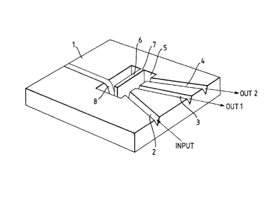
The optical element or assembly shown in the
drawing includes a substrate comprising a single crystal
silicon slice 1 in the upper surface of which three V-
shaped grooves 2-4 have been etched using an anisotropic
masking and etching technique. The grooves 2-4 all have
substantially the same depth and are effectively coplanar.
~S Each groove 2-4 termina-tes in a cavity 5 formed in the
; substrate 1. Monomode optical fibres (not shown) are
positioned in each of the grooves 2-4 with their ends
facing into the cavity 5.
A cantilevered, vertically hinged silicon beam 6
is positioned in the cavi-ty 5 and is integrally formed
with the remainder of the substrate 1. The beam 6 acts as
an optical reflector.
The beam can pivot about its end 7 between first
` and second positions in response to an electrostatic field
generated by a pair of electrodes, one of which 8 is
- mounted to the substrate and the other of which is


B


.,


; mounted to the facing surface of the beam 6. If the beam
is at ground potential, the second electrode is not
required. The electrodes are connected to electrical
control apparatus including a power source ~not shown~.
In its first position, the reflector 6 reflects
optical radiation passing along the optical fibre in the
;~ groove 2 into the optical fibre in the groove 3. In its
second position, optical radiation impinging on the
reflector 6 from the fibre in the groove 2 is reflected
l~ into the fibre in the groove 4. The element shown in the
drawing can thus be used as an optical switch to switch
incoming radiation in the optical fibre in the groove 2
into eithex the optical fibre in the groove 3 or the
optical fibre in the groove 4.
: 15

.~

: ~n


. 30


:``


. ~ .
.
. .

. .

Representative Drawing
A single figure which represents the drawing illustrating the invention.
Administrative Status

For a clearer understanding of the status of the application/patent presented on this page, the site Disclaimer , as well as the definitions for Patent , Administrative Status , Maintenance Fee  and Payment History  should be consulted.

Administrative Status

Title Date
Forecasted Issue Date 1991-05-21
(22) Filed 1986-10-17
(45) Issued 1991-05-21
Deemed Expired 1995-11-21

Abandonment History

There is no abandonment history.

Payment History

Fee Type Anniversary Year Due Date Amount Paid Paid Date
Application Fee $0.00 1986-10-17
Registration of a document - section 124 $0.00 1990-10-17
Maintenance Fee - Patent - Old Act 2 1993-05-21 $100.00 1993-04-13
Maintenance Fee - Patent - Old Act 3 1994-05-23 $100.00 1994-04-15
Owners on Record

Note: Records showing the ownership history in alphabetical order.

Current Owners on Record
STANLEY, IAN W.
BRITISH TELECOMMUNICATIONS PUBLIC LIMITED COMPANY
Past Owners on Record
None
Past Owners that do not appear in the "Owners on Record" listing will appear in other documentation within the application.
Documents

To view selected files, please enter reCAPTCHA code :


To view images, click a link in the Document Description column. To download the documents, select one or more checkboxes in the first column and then click the "Download Selected in PDF format (Zip Archive)" or the "Download Selected as Single PDF" button.

List of published and non-published patent-specific documents on the CPD .

If you have any difficulty accessing content, you can call the Client Service Centre at 1-866-997-1936 or send them an e-mail at CIPO Client Service Centre.


Document
Description 
Date
(yyyy-mm-dd) 
Number of pages   Size of Image (KB) 
Drawings 1993-10-20 1 17
Claims 1993-10-20 2 66
Abstract 1993-10-20 1 22
Cover Page 1993-10-20 1 16
Description 1993-10-20 4 157
Representative Drawing 2002-03-20 1 7
Fees 1994-04-15 1 102
Fees 1993-04-13 1 44