Note: Descriptions are shown in the official language in which they were submitted.
36
TIT:~.E C)F Ti~E INVE,MTI 01~
Melnbe~ for Semicorlductor Appardtus
BACKGROUND ~F THE INVENTION
Field of the Invention
The present invention relates to a member for a
semi~onduc-tor apparatus, and mo~e parti.cularly, it relates
to a member for a semiconductor apparatus such as a
c.ircuit substrate, which must be of high thermal
conductiv.ity to be mounted w.ith a semicorlduc~or de~ice oE
high caloxi~ic pow~r such as a high-power tx~nsistor or a
laser diode.
Description of the Prior Art
A member for a sem~conductor apparatus to be mounted
with a semiconductor device is generally formed by an
insulating member and a radiating member joined to the
insulating member. For example, such a member for a
semiconductor:apparatus is formed by an insulating
substrate to be provided thereon with a sem.icondu~tor
device and a :radiating.substrate joined to the.back
surface of the insulating substrate by soldering through
silver solder or the li.ke. In this case, gerJerally
re~uired for the ins~llating substrate are high electric
insulability for insulation from the semiconduct~r device,
high mechanical strength and high.thermal con~uctivity Eor
dissipating heat.generated from the.semiconductor-device.
3L~ 6
The radiating substrh~e must have hiyh thermal
conductivity simi.larly to the .insulating substrate, w~lile
its thermal expansion coefficient must be approximat-e to
those of materials forming a semiconductor substrate, the
insulating substrate and the like.
In general, alumina.(A12O3) is selected as a material
satisfying the aforementioned properties for formi.ny the
insulating substrate employed in.such a member for a
semiconductor apparatus. However, although al~nina is
excellent in electric insulability and mechanical
strength, its he-at dissipation property is inferior due-to
small thermal conductivity of 17 Wm lK 1. Thus, it is
improper to carry a field-effect transistor (FET) of.high
calorific power, for example, on an alumina substrate; In
order to carry a semiconductor device of high.calorific
power, another type of insulating substrate is prepared by
beryllia (BeO) having high thermal.conductivity of 260
Wm K , whereas beryllia is toxic and hence it is
troublesome to take safety measures in employment of such
an insulating substrate.
The radiating.substrate .is generally prepared by a
material satisfying the aforemention~d properties, which
material is selected from metal materials such' as various
types of copper alloys, copper-tungstén alloys and
copper-molybdenum alloys. For example, Japanese Patent
Laying-Open Gazette No. 21032/198~l discloses a sub~trate
of high thermal conductivity for carrying a semicondllctor
device, the material of which is prepared by mixi.ng 2 to
30 percent by weight of copper into tungsten or
molybdenum. This substrate is employed as a radiating
substrate which is suitably joined to an alumina substrate
having inferior heat dissipation property, and differencs
in thermal expansion coefficient between tlle same and
alumina is relatively-small. Thus, t~lis prior art e~ampls
is.insufficient in heat dissipation property, which is
required entirely over a substrate for carrying a
semiconductor device.
In recent years, nontoxic aluminum nitride tAlN) has
generated great interest as a material for such an
insulating substrate for carrying a semiconductor device
of high calorific power because of its high thermal
conductivity of about. 200 Wm 1K 1, which value is
substantially e~ual to that of beryllia> as well.as..its
electric insulability and mechanical strength which are
equivalent to those of alumina.
However, when an aluminum.nitride substrate provi.ded
with a metallized layer is soldered by a soldering metal
such as gold solder or silver solder, for example, to a
generally employed radiating substrate.of a
copper-tungsten alloy or copper~molybdenum alloy
contain.ing ln to 25 percent by weight of copper, lrhe
aluminum oitr.ide substrate may be cracked or the radial~ g
substrate of the copFer-tungsterl alloy or the
copper-molybdenum alloy-may be warpe~.
Such a phenomenon results f rom thermal stress caused
by difference in therma~l expansion coe~ficient~ between the
copper-tun~sten alloy or the copper-moJ ybdenum alloy and
alurninum nitride during a cooling step UpOll soldering,
which is performed at a ternperature of 500 to 9~0C. Thi.~s
10 thermal stress may conceivably be lef t in the alurninum
nitride substrate as tensile residual stress, to crack the
aluminurn nitride- substrate and/or warp the radiating
substrate of the copper-tungsten alloy or the
copper-molybdenurn alloy.
When an alurninum nitride substrate is joined to a
radiating substrate of a copper-tungsten alloy or a
copper-molybdenum alloy by cold soldering or soldering,
the alumi.num nitride subs.trate or an interf ace between the
same and a metallized layer is cracked by a therrno cycle
20 tesl~ ~-55C to +150C, 1000 cycles) or a thermal shocl~
tes t to cause a signif icant problern in practice, even if
no warp nor crack. is recognized upon joining.
In a sample of an aluminum nitride substrate joined
to a radiating substrate of a copper-t.ungsten alloy or a
25 copper-molybdenum alloy by silver soldering, therma~l
f~
~atigue or thermal st~ess was caused in a t}lermo cycie
test or a thermal shoc~ test due to d.iffelence in thern)al
expansion coefficient between the radiating substrate of
the copper-tungsten alloy or the copper-molybdenum alloy
S and the aluminum nitride substrate, similarly to the
above. Such a problem of thermal stress or thermal
fatigue is aggravated with increase in junction-area.
Thermal expansion-coefficierlts of the copper-tungsten
alloy or the copper-molybdenum alloy having.the
aforementioned composition and aluminurn nitride are 6.5 to
10 X 10 6IK and 4 to 5 x 10 6/K respectively, within a
ranye of the room temperature to about 950C. Further,
these materials, having high Young's modulus of 27000 to
35000 KgJmm2 and 35000 to 37000 Kg/n~2 respectively, are
~lardly plastically deformed. Thus, when the
copper-tungsten alloy or the copper~molybdenum alloy of
the aforementioned composition:and.aluminum nitride are
joined with each other by soldering, large thermal.stress
is conceivably caused in a cooling step.
SUMMARY OF THE INVEN~'ION
An object o~ the present invention is to provide a
member for a semiconductor apparatus by employing an
insulating member of alumin.um nitride, being excellent in
thermal dissipation property, for mounting a semiconductor
device of high balorific power, so that a radiating memb2r
.
L~
mainly ~ormed of a cop~er-tullgsterl.alloy or a
copper molybdenum alloy having~high heat radi.ation
property can be joined to the insulatiny member while
causing no crack nor warp.
The inventors have made deep study to solve the
aforementioned problem, to Eind that it is effective to
interpose a specific thermal.stress.relieving member
between an insulating member.of aluminum nitride and a
radiating mem~er mainly formed of a copper-tungsten~alloy
or a copper-molybderlum alloy, to prevent cracking or
warping caused by thermal stress in a cooling step upon
soldering.
A member for a semiconductor apparatus in accordance
with the present invention, being.adapted to carry or hold
a semiconductor devicej comprises an insulating.member oE
aluminum nitride having a major surface to face the
semiconductor device, a radiating member to be joined to
the insulating member and mainly Eormed oE a
copper-tungsten alloy or a copper-molybdenwn alloy, a
stress relieving.member, and a soldering.member for
joining the insulating member, the stress relieving member
and the radiating member with each other. The stress
relieving member, to be interposed betweeT~ the insulating
member and the radiating member, is prepared by a soft
z5 metal or a soft alloy having high plastic deformability in
order to relax, throuyll its own plastic deEoLmation,
thermal stress caused by differencQ in t~lermal expansion
coefficient between the insulating member and the
radiating member in a cooling step upon soldering.
Preferably the stress.reli.eving member is prepared by
copper, a copper alloy, nickel or a nick~l alloy.
The stress relieving member of either a soft metal.or
a soft alloy-thus interposed between the insulating member
of aluminum nitride and the radiating memher is further
softened around the soldering temperature, to be extremely
plastically deformable~ Thus., most part of thermal ~stress
caused by difference in thermal.expansion coefficient
between the insulating member of aluminum nitride and tlle
radiating member is absorbed by plastic deformation.of the
stress relieving member, to solve the problem of residual
stress in the insulating member. Consequently, the
insulating member is prevented from cracking and the
radiating member is prevented from warping.
The stress relieving member is preferably in a range
of ~.~1 to 1 mm in thickness. If the thickness is not
more than 0.01 mm, the stress relieving member cannot be
sufficiently plastically deformed to absorb thermal
stress. If the thickness exceeds.1 mm, on the other-hand,
thermal stress caused.by thermal expansion of the stress
relieving member itself in soldering cannot be neglected..
Namely, although thermal stress caused by difference in
therrnal expans.ion coefficient betweell tl,e radiating mernb~r
and the insulating member can be ab,orbed by plastic
deformation of.the stress relieving memher, the stress
relieving member itself causes significant thermal stress
to exert bad influence of thermal deformat.i.on on the
radiating member or the insulati.ng member.
The insulating member of aluminum nitride is
preferably employed as a substrate having a major surface
to be provi.ded.thereon.with a semiconductor device.
Alternatively, the insulating member m~y be applied to a
covering member. provided above a semiconductor device to
protect the same, which covering member forms a cap for
airtightly sealing a semiconductor device provided on an
insulating substrate, for example. When the insulating
member is employed as a substrate for carrying:a
semiconductor device or a covering member for protecting-a
semiconductor device, the inventive member for a
semiconductor apparatus is adapted to conduct heat
generated from the semiconductor device to the insulating
member and a radiating mem~er, thereby to dissipate the
same to the exterior. The insulating.memb.er of aluminum
nitride preferably includes a sintered body.
The insulating member.of alumlnum nitride is
preferably provided on its junction surface with a
-- 8
metallized layer, which contains ~t least tullgsten or
molybdenum, at least one aluminum compound within aluminum
nitride, aluminum o~ide-and aluminwn o~ynitride, and
calcium oxide or yttri~lm o~ide, to attain preferable
junction strength and thermal conductivity.
Further, a plating layer is provided in a junction
surface of the metallized layer with a soldering member to
uniformly perform stabilized soldering. Namely,
wettability between the soldering member and the
metallized layer can be improved by provision of the
plating layer. Another plating la~er provided in a
junction surface of the radiating member with the
soldering member functions similarly to the above. Such
plating layers are preferably formed by nickel plating.
Such nickel plating is preferably performe~ particularly
when processing such as gold plating is performed in a
later step, in order to improve adhesion and precipi.tation
properties of gold plating for forming a uniform gold
plating layer.
Further, the copper-tungsten alloy or the
copper-molybdenum alloy employed for the inventive member
preferably contains 5 to 25 percent by weight of copper.
If the content of copper is less than 5 percent by weight,
thermal conductivity, being an essential function of the
copper-tungsten alloy or the copper-molybdenum alloy
3~
forming the radiating rnembe-, may be lost althougll
mismatch in therma~ expa~sion coefficient between the
copper-tungsten alloy or the copper~molybdenum alloy and
aluminum nitride is relaxed. 1~ ti-le content of copper
exceeds 25 percent by weight, the thermal expansion
coefficient of the copper-tungsten alloy or.the
copper-molybdenum alloy is further increased to diEfer
from that of aluminum nitride, leading to increase in
thermal stress caused.in the junction surface, although
thermal conductivity of the copper-tungsten alloy or the
copper-molybdenum alloy is rendered urther preferab'e.
According.to the inventive member for a se~iconduct.or
apparatus, a stress relieviny member is interposed between
the insulating member and the radiating.member, thereby to
prevent cracking.of the.insulating membex and warping of
the radiating member upon joining of the insulating.member
of aluminum nitride and the radiating mem~er mainly formed
of the copper-tungsten alloy or the copper-molybdenum
alloy. Thus, a reliable:member for a semiconductor
apparatus.can be easily obtained to be applied to a
substrate for carrying a semiconductor apparatus, a
covering member for sealing a semiconductor device or the
like.
These and other objects, features, aspects and
advantages of the-present invention will become more
-- 10 --
,, . , ;
3 ~
apparent from the following-detailed descriptiorl of the
present invention when taken in conjunc-tion- Wit~l the
accompanying drawings.
BRIEF DESCRIPTION OF THE DRAWINGS
Figs. lA and lB are process drawings schematically
showing two exemplary methods of manufacturing a rnember
for a semiconductox apparatus in accordance with the
present invention;
Figs. 2A, 2B and 2C are a plan view and sectional
vi~ws showing an example oE junction structure in a member
for a semiconductor apparatus in accordance with the
present invention, such as jw~ction struct-lre between a
lead frame, an aluminum nitride substrate and a radiating
substrate;
Fig. 3 is a sectional view showing an embodiment of a
member for a semiconductor apparatus in accordance with
the present invention, which is applied to a heat sink
mernber for a semiconductor devi.ce such as a light emitting
diode (LED) or a laser diode tLD);
Fig. 4 is a sectional view showing another embodiment
of the inventive member for a semiconductor apparatus,
which is applied to a part of a cap for airtightly sealing
a semiconductor device to serve as a covering member; and
-- 11 --
Fig. 5 is a side elevational view.show~3ng a porti.on
subjected to measu.rernent of a warp caused in a radiating
member joined to an aluminum nitride substrate.
DESCRIPTION OF THE PRE~FERRF~D EMBODIMENTS
S As hereinabove described, the present invention is
adapted to improve the technique of formin~ a member for a
semiconductor apparatus by employing.an insulating.member
of aluminum nitride~ Aluminum nitride employed in the
form of a sintered body in the present inven-tion is
obtained by the following method, for example:
The insulating member ~ormed by an aluminum nit~ide
sintered body employed in the present invention,
preferably being mainly composed.of aluminllm nitride,
contains 0.01 to 1.0 percent by weight o~ an element
belonging to the group Illa of the periodic table and
0.001 to 0.5 percent by weight o oxygen, and its thermal
conductivity is at least 180 Wm 1K 1. First, at least one
compound containing a rare earth element is mixed with
powder of aluminum nitride so that its content is 0.01 to
1.0 percent by weight in rare earth element conversion. A
~orming additive.is prepared by paraphine, PVD or PEG. A
substance, such as phenol resin, being decomposed to leave
carbon, carbon powder, graphite powder or.the like may be
added to control residual carbon.in the sintered body.
The rare earth compound is prepared by stearic acid,
- 12 -
palmitic acid, alkoxide nitrate, carbonatc, hydroxide or
t~e like. Preferably employed is a high molecule compoulld
such as stearic acid. Such a compound is conceivably
adapted to reduce the content oE the rare earth elem~nt to
enable good mixing with aluminum nitride powder. In
particular, stearic acid is JnoSt preEerable in view~of
mixability with aluminwn nitride powder, the amount of
residual carbon etc~ in addition to its function as a
formir)g additive. The alumirlum nitride pow~er must be
Eormed by fine uniform particles. Preferably its average
particle size is not more than 1 ~m, and the oxygen
content is not more than 2.0 percent by weight. Such
aluminum nitride powder is obtained by a reduction
nitriding method ~method by reduction nitriding of
aluminum oxide), since it is difficult to obtain the same
by a direct nitriding method (method by nitriding of metal
aluminum). In order to obtain the powder by the direct
nitriding method, sufficient considerati.on must be made on
reaction control, classification of the particle size and
the like.
Then the mixed powder is shaped into a prescribed
configuration and sintered in a non-oxidizing atmosphere
containing nitrogen. In order to attain high thermal
conductivi.ty, it is preferable to sinter the substance at
a temperature of 1000 to 2100C for at least five hours,
~ h~-~
so that its average part.icle si~e i~s at least 5 ~)m. A~e-r
such sintering, .i-t is prefera~le to quickly carry ouL a
cooling step. If the subs~ance is slow-ly cooled, a
sintering additive is precipitated and the sintered face
is extremely deteriorated. Therefore, -the sintered body
is preferably cooled to a temperature of 150~C at a rate
o~ at least 200C/h.
The steps of forming a metallized layer on the
surface of a substrate formed by thc aluminum nitride
sintered body obtained in the aforementione~ manner are
performed as follows:
First, a substrate of the aluminum ni~ride sintered
body is prepared by the aforementioned method. A material
for-the metallized layer is prepared by kneading powder of
a calcium compound, that of an alwninum compound and metal
powder of tungsten or molybdenum with addition.of:an
organic binder.such.as vehicle, to provide metal paste.
The contents of the respective components may be within
the ranges of 40 to 98 percent by weight o~ the metal
powder, 1 to 25 percent b~ weigh.t of the aluminum compo-lnd
and l to 35 percent by weight of calcium oxide. In order
to perform a later sintering step at a low temperature,
copper or nickel ma~ be added.as a catalyst for reducing
the sintering temperature. The metal paste thus provided
is applied to the surface of the substrate formed by the
- 14 -
al~ninum nitride sintexe~ body. The-su~s~rate formed by
the aluminum nitride sinter.ed body is fired in an inert
atmosphere of nitrogen or the like at a temper~ture.-of
1500 to 1800C, to be provided with a metallized layer ~n
its suxface. A metallized layer prepared by metal powder
of tungsten and containing 1 to 10 percent by weight of
aluminum oxide, employed as the aluminum compound, and 1
to 20 percent by weight of calcium oxidej or that prepar.ed
by metal powder of molybdenum and.containing 1 to 10
percent by weight of aluminum oxidej employed as the
alumi.nwn compound, and 1 to 35 percent by weight. of
calcium oxide is preferable in view of adhe~ion betwe2n
the substrate formed by the aluminum nitride sintere~ body
and the metallized layer and thermal conductivity.
The steps of forming a metallized layer on the
su~face of a substrate formed by the aluminum nitride
sintered body may be.performed as follows, by sintering.an
aluminum nitride formed body coated with the metal paste
at one time.
First, a substrate of the aluminum nitride formed
body is prepared by shaping the aforementioned mixed
powder into a prescri.bed configuration such as a green
sheet. A material for the metalli7.ed layer is prepared by
kneading powder of tungsten and at least one additive
25 selected from a group of aluminum oxide, aluminum nitride,
- 15 -
f~
calcium oxide, yt~rium oxide and stearic acid yt~rium and
the like, to provide metal paste, similarly to the above.
The metal paste thus pro~ided is applied to the surface of
the substrate formed by the aluminum nitride formed body,
by printing or coating. The substrate formed by the
aluminum nitride formed body is sintered with the metal
paste similarly to the above conditions, to be provided
with a metallized layer on the-surface-of a substra-te
formed by the aluminum nitride sintered body. Thus, the
aluminum nitride sintered body with the metallized having
high thermal conductivity can be obtained.
Description is now made on a typical method of
forming the member for a semiconductor apparatus in
accordance with the present invention. Figs. lA and lB
are process drawings showing two methods of manufacturing
the member for a semiconductor apparatus in accordance
with the presenk invention. Referring to Fi~. lA, an
aluminum nitride sintered substrate is first prepared.
Then, the metal paste obtained through the aforementioned
method is applied to the surface of the aluminum nitride
sintered substrate. Thereafter the metal paste thus
applied is dried. Then the aluminum nitride sintered
substrate is fired in an inert gas atmosphere which is
heated to a prescribed temperature.
- 16 -
~L,~
The above steps may be performed as follows.
Referring to Fig. lB, an aluminum nitride formed substrate
is first prepared. Then, the metal paste obtained through
the aforementioned method is applied to the surface of-the
aluminum nitride formed su~strate. Thereafter the metal
paste thus applied is dried. ~hen the aluminum nitride
formed substrate is sintered with the metal pa~te in an
inert gas atmosphere which is heated to a prescribed
temperature. Thus, an aluminum nitride sintere~ substrate
with a metallized layer is formed.
After a metallized layer is formQ~ on the aluminum
nitride sintered substrate, nickel plating is performed on
the surface of the metalliæed layer. Heat treatment is
performed at a temperature of about 800C to sinter the
lS nickel plating, thereby to improve strength and
airtightness of the same. On the other hand, nickel
plating is also performed on the surface of a heat sink
member, serving as a radiating member, which is joined to
the aluminum nitride sintered substrate, similarly to the
above. Then soldering is performed on the nickel plating
surface in order to join the aluminum nitride sintered
substrate to the heat sink member. Further, gold plating
is performed on such junction. Thus, the member for a
semiconductor apparatus in accordanae with the present
invention can be manufactured.
- 17 -
Description is now made on an embodiment of a member
for a semiconductor apparatus in accordance with an aspect
of the present invention, which is manufactured along the
aforementioned steps, such as a member comprising an
aluminum nitride substrate joined to a lead frame on its
surface and to a heat sink member on its back surface,
with reference to the dxawings.
Fig. 2A is a plan view showing an embodiment which is
applied to a substrate for carrying a semiconductor
device, Fig. 2B is a sectional view of the substrate and
Fig. 2C is a sectional view showing a junction between a
heat sink member 6 and an aluminum nitride substrate 1 in
detail. Referring to these figures, the aluminum nitride
substrate 1, implementing the inventive member-for a
semiconductor apparatus, is partially formed on its
surface with a metallized layer 2 in accordance with the
aforementioned steps, and a lead frame 3 is joined to the
metallized layer 2 through soldering by a soldering metal
or the like. Another metallized layer 2 is formed on a
ZO part of the back surface of the aluminum nitride substrate
1 in accordance with the aforementioned steps, while the
heat sink member 6 is joined to the metallized layer 2
through soldering by a soldering metal or the like. A
semiconductor device 4 such as an FET of high calorific
power is carried on a prescribed Fosition of the aluminum
- 18 -
' ' ~ ' ' '" ' '~ .- .
nitride subs~rate 1, to be conllected wi~h the rneLallized
layer 2 or the lead ~rame 3 by a bondir.g wire ~. As shown
in Fig. 2C, a thin plating layer.7 is formod on t.he
metallized layer 2 in the junction between-the aluminum
nitride substrate 1 and the heat sink member-6, while a
plating layer 3 is formed at need on the surface oE the
heat sink member 6, in order to stabilize wettability of a
soldering metal 9. In this case, a stress relieving
member 10 of a soft metal such as copper, which is formed
with nickel plating layers 7 on its surface, is interposed
between the metallized layer 2 and the heat sink member 6
serving as a radiating member.
Description is now made on another embodi~ent of a
member for a semiconductor apparatus in accordance with
another aspect of the present invention, which is applied
to a radiating substrate for carrying a semiconductor
device such as a diode having high calorific power, for
example, with reference to Fig. 3. Referring to Fig. 3,
an aluminum nitride substrate 1 is mounted on a heat sink
member 6, serving as a radiating member mainly formed of
the copper-tungsten alloy or the copper-molybdenum alloy
in accordance with the present invention~ through a
metallized layer 2 similarly to the above, while a
semiconductor:device 4 such as a light emitting diode
(LED) or a laser diode (LD) is joined on the aluminum
19 -
nitride substrate 1. The semicondu,tor device 4 is joined
on another metallized layer 2 which is formed on the
surface of the aluminum nitride substrate 1. In this
case, the aluminum nitride substrate 1 serves as a heat
sink member. The alwninum nitride substrate 1 and the
heat sink member 6 are joined with each other in a similar
manner to the above description with reference to the
junction structure between the aluminum nitride substrate
provided with the lead frame and the heat sink member.
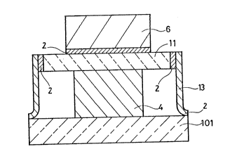
Description is now made on the structure of a cap to
which a member for a semiconductor apparatus in accordance
with the present invention is applied, with reference to
Fig. 4. A metallized layer 2 is provided on the surace
of a peripheral edge~portion of a covering member 11
formed by an aluminum sintered body. A frame-member 13
formed by a layer of a metal such as an iron-nickel alloy
is joined to the metallized layer 2 by a soldering metal
or the like. The lower end of the frame member 13 is
joined to a ceramic substrate 101 through another
metallized layer 2. A semiconductor device 4 is carried
on the ceramic substrate 101. A heat sink member 6 is
mounted on the upper surface of the covering member 11, so
that heat generated from the semiconductor device 4 is
dissipated by the heat sink member 6 through the covering
member 11, to improve a cooling effect. The covering
- 20 -
r~3L~
member 11 of the aluminum nitride sintere~ body and the
heat sink member 6 are joined w.ith each other in a similar
manner to the above description with reference to the
junction structure between the aluminum nitride substrate
provided with the lead frame and the heat sink member.
The soldering metal employed for such junction is
preferably prepared by silver solder, while another
soldering material.is also available so far as a thin
metal coating layer having good wettability to the
soldering material can be formed on the junction surEace
of the heat sink member 6 or the metallized layer 2 to
strongly join the covering member 11 and the-heat sink
member 6 with each other. The function of such a thin
metal coating.layer, such as a plating layer, is as
hereinabove described with reference to the example of
junction structure-between the aluminum nitride substrate
provided with the lead frame and the heat sink member.
Descript:;on .is now made on Examples 1 and 2 of the
present invention, which were made by sa.mples prepared by
substrates of the aluminum nitride sintered body obtained
by the aforementioned method.
Example 1
Aluminum nitride sintered substrates of 1 . 3 mm iII
thickness were prepared by the aforementioned method, to
be subjected to metallization. The metalliz.ation
- 21 -
processing was perf~rmed by applying metal pas~e oE
prescribed composition to the surfaces of respective
samples of the aluminum nitride sintered substrates,
performing debindering and then Eiring the same in a
nitrogen atmosphere at a temperature of 16~0C fox 60
minutes. Thus, metallized layers were formed on
prescribed portions of the aluminum nitride sinte.red
substra~es. The metal paste was prepared by adding
calciurn oxide powder and alurnina powder to tungsten powder
and kneading the same with an organic binder such as
vehicle. The conteTlt of ca.lcium oxide.was 14 percent by
weight and that of alumina was 4 percent by weight. The
shapes of the employed aluminum nitride sintered
substrates were 5 mm square, 20 mrn square and 50 mrn s~uare
respectively.
Further, nickel plating layers of 2 ~m in thickness
were formed on the surfaces of the rnetallized layers. On
the other hand, copper-tungsten alloy plates oE 1.5 mm in
thickness having various compositions.were prepared as
radiating members to be joined to the respective aluminum
nitride sintered substrates. Nickel plating of 2 ~m in
thickness was performed on the surfaces of these
copper-tungsten alloy plates, which were then soldered to
the respective aluminum nitride sintered subs.t-rates ~y
- 22 -
~rP~
silver solder with interposi.tion o~ stress relieving
members of nickel or coppex at, a tempera.ture of 830C.
Examination was.made as to whet.he~ or not the
aluminum nitride sintered substrates were cracked and
whet~,er or not the cop~er-tungsten alloy plates were
warped in the respective samples thus obtained. As shown
in Fig. 5, an aluminum nitride sintered substrate 1 and a
heat sink member 6 of each sample were joined with each
other, to evaluate the degree of wa.rping as the amo~lnt a
by a surface roughness tester (product of Tokyo Seimitsu:
E-SP-SOlA). Cracks caused in the respective aluminum
nitride sintered substrates were obser~ed by a scanning
type electron microscope of 5000 magnifications or a
steromicroscope o~ 40 magnifications. Tables 1 to 3 show
the results. As to evaluation of warps, those oE not more
than 2 ~m with respect to effective length of 1 rnm were
regaxded as l~X10 warp", while samples causing warps
exceeding 2 ~m with respect to effective length oE 1 mm
were regarded as "warped".
The numerals 5, 10 and 20 in "CuW5", "CuW10" and
l'CuW20" in Tables indicate contents.of copper in the
copper~tungsten alloys. As to the copper-tungsten alloys,
thermal expansion coeffi.cients of CuW5, CuW10 and CuW20
were 6.0 to 7.0 x 10 6JK, 6.5 to 7.5 x 10 6/K and 8.5 to
25 9.5 x 10 ~K in a range of the room tempera-ture to 950C.
- 2~ -
Further, values of thermal conductivity of CuW5, CuW10 and
CuW20 were 180 ~mKr 210 W~mK and 246 W~'mK respectively
The wording."cracked'` in Tables indicates that cracks
were caused i~ the interiors of the aluminum nitride
sintered substxates.
Similar evaluation was also made on reference
examples including no interposed layers serv~ng as stress
relieving members. Table 4 shows the results.
According to Table 1, no crack nor warp was
recognized in samples having interposed layers-, serving as
the stress relieving.members in accordance with the
present inventionj of at least 100 ~n in thickness.
According to Table 2, no warp nor crack was recoynized in
samples having.interposed layers of 500 ~m in thickness.
According to Table 3, no crack nor warp was rec~gnized in
samples having interposed layers of 1000 ~m in thickness,
while those having.interposed layers o~ less.than and in
excess of 1000 ~m in thickness presented cracks and./or
warps. As shown in Table 4, all samples of reference
examples, including no interposed layers for.serving as
stress relieving members, presented warps and/or cracks.
-
- 24 -
T~ e 1 ( O S ~
_____ _
Interpo~ed Layer Cu Cu L,ayer wiLh Ni
Or_N;__ _ __ _ PlalilJg of ~_~m
of ~ r- CuWS ; cu~o CuW20 CuW5 cuwin CuW20 CuW~ CuW10 C~nW20
L yer warped warped warped no warp warped warped no warp no warp w~rped
_ _ _ .___ _ _ __ _ .. _._ I_ _ _ _ __.
100 ~m no warp no warp no warp r,o warp no warp no warp no warp no warp no w~rp
___ ._ _ __ _ _ ._ . ..._. ._ _ _.. .... __ _ __ . _ . _ _ . _ _
. 500 ~m no walp no warp 110 warp no war~ no warp no w~rp no warE~ no warp no war~
Tab.le 2 (~ 20 mm)
_ _ . _ .
Interposed Layer Cu Cu Layer w;t~ Ni
o~ Ni_ _ _ ___ __ __..__ __. . _ __. _._ Plat;nc _oE ~
'I'hickness CuW5 CuW10 Cu~20 CuW5 CuW10 CuW20 CuW5 Cu~10 CuW20
of Inter-
, _ _ _
10 ~m warped warped wa.rpe~ warped warped warped warpea warpe~ warp~d(crack- (crack- ~cr~ck- ~crA(k-
ecl) ed) ed) ~d)
100 ~m no warp warped warped no warp warped warpea no warp no war~ wa.rp~d
S00 ~m no warp no wa.~p no warp no warp no warp no warp no warp no warE~ n~ wa~E
- 25 -
Table 3 ~ S~ mm)
Il~terE~sed L~y~ C~l C~ I.aye~ ~;lh
of Ni l'latin of
Thichness C~WS CuWlO Cu~20 C~IWS C~WlO C~W20 CuWS CuWl~ ~IW~
I _ _ _ ___ ___
100 ~m w~rped wal~ped w3rped warp~d warped w3r~ea warp~ warped w~rp~l
(crack- (crack- (crack- (crack- (crack- (crack- (crack- (crack- (crack-e-l) ed) ed) ¦ed) led) ed) ~d) ed) ed)
500 l~ warp~d warped warp~ n~ w~rp ~arr!~d war~e~3 no warF n~ wlr~ .~rp~d _ _ ( r~oh-
1000 ~ no warp no warp 110 W3rF no warF no warp no w~rp nc> warp no warp 110 w~r~
, I _ l500 ~m no warp no warp no warp no warp no warp no warp no warp no warp no warp
(crack- (crack- (crack- (crack- ~crack- ~crack- ~crack- ~crack- ~c~c~-
ed) ed) ed) ed) ed) ed) ed) e~) ed)
Table 4 (Reference Example)
_ _ _
CUW5 CuW10 CuW20
__ ,_~ I
5 mm warped warp~d warped
(craeked)(eracked)
I_
a 20 mm ~arped warped warped
(cxacked) (cracked)(cracked)
I_ I
a ~o ~n warped warped warped
(cracked) (cracked!(cracked)
Example 2
Samples of alumin~n nitride sintered substrates with
metallized layers were prepared by the aEorementioned
method as shown in Fig. lB. The metallization processj.n~
- 26 -
of sam~les was perfol-med by app~yiny tungstell paste of
pxescribed composi.tion. to the surfaces of respecti.ve
samples of the aluminum formed substrates shaped in a
configuration such as a green shee~ by the aEorementioned
method with screen printing of prescribed patterns,
drying, performing debindering and then sintering the s~ne
in a nitrogen-hydrogen atmosphere at a temperature of
1850C for 5 minutes Thus, metallized layers were formed
on prescribed portions of aluminum nitride sintered
substrates. The shapes of the employed aluminum nitride
sintered substrates with metallized layers were 5 mm
square, 20 mm square and 50 mm sguare of 1.5 mm in
thickness respectively.
Further, nickel plating layers were formed on:the
surfaces of the metallized layers, simi.larly to Example 1
On the other hand, copper-molybdenum alloy plates of
1.5 mrn in thickness having various compositions:were
prepared as radiating members to be joined to.the
respective aluminum nitride.sintered.substrates. Nickel
plating of 2 llm in thickness was performed on the surfaces
of these copper-molybdenum alloy plates, which were then
soldered to the respective alumi.num nitride sintered
substrates by silver solder with interposition of stress
relieving members of nickel or copper in a hydrogen
atmosphere at a temperature of 830C.
- 27 -
~ sb~ ~ 6
Examination was made as to cxacks of the aluminnm
nitride sintered subs~rates and warps of the
copper-molybdenum alloy plates similarly to Example 1.
Tables 5 to 7 show the results.
The numerals 10, 15 and 20 in "CuMolO", "CuMol5" and
'ICuMo20`' in Tables indicate contents of copper in the
copper-molybdenum alloys. As to the copper molybdenum
alloys, thermal expansion coefficients of CuMolO, C~1015
and CuMo20 were 6.4 to 6.8 x 10 6/K, 7.0 to 7.4 x 10 6/K
and 7.6 to 8.3 x 10 6/K in a range of the room temperat~ e
to 950C. Further, values of thermal.conductivity oE
CuMolO, CuMol5 and CuMo20 were 165 W/mK, 184 W/mK and
196 W/mK respectively.
Similar evaluati.on was also made on reference
examples includiny no interposed layers serving as stress
relieving.members. Table 8 shows the.resul.ts.
According to Table 5, no crack nor warp was
recognized in samples having.interposed layer, serving as
the stress relieving.members in accordance.with the
present invention, of at least 100 ~m in thickness.
According to Table 6, no warp nor crack was recognized in
samples.having interposed layers of 500.~m in thickness.
According to Table 7, no crack nor warp was recognized in
samples having interposed layers of 1000 ~m in thickness,
while those having interposed layers of less than and in
- 28 ~
excess of 1000 ~ in th.ickness presente~ cracks and/or
warps. As shown in Table 8, all sample~ o~ reference
exc~nples, including no interposed layers for serving as
stress relieving members, presented warps and/or-cracks.
~ 5 (U~- mln)
_. _
Interposed Layer Cu C'u Layer wit}, ~i
of Ni _ ~latil) c, ~
Thi<:kne~s CuMolO CuMc~5 CUM~20 1 CuMolO C'uMol.'i CuMo20 Cu~olO CuMolS C~o20
Lay r
10 ~m warped warped warped warped warped warped no warp no warp no warp __
100 ~m no warp no warp no warp no warp no warp rlo warp no warp n~ warp n~ warp
_ _
500 ~m no warp no warp no warp no warp no warp no warp no warp no warp no W~rE'
_
Tc~ble 6 (D 20 n~)
Interposed Layer Cu Cu Layer w.ith ~i
of N. _ ____ _ _ __ _ _ Pla~in~ _o~_~_Lm
Thickness CuMolO CuMol5 CuMo20 CuNolO CuMolj CuMo20 CuMolO C'uMol5 CuMo20
of Inter
_ I
10 ~m warped warpe~ warpea warpe~ warpe~ warped warp~ war~e.~ warp~d
(crack- ~ crac:k- ( crack- (craok- (crack- (crac:k (cra~k
ed) ed) ed) ~d) ed) ed) ed)
1- -- I -- _
100 ~m warped ¦warped warped warped warped warpe~ wc~rped- warped w~ped
SOO ~m no warp no wc~rp no warp no warp no warp no warp no warp no w~r~) no W~l p ¦
-- 29 --
~,P'~ ~6
Tc~Ie 7 (~ 50 mm)
_ Interpos~.1 Lay~r Cu r,~ J,~y~-- wi~h Hi
~f_N~ Iatinc oE ~ lul I _
Thickne~ CuMolO ~ Hol5 CuMo20 CuMolO CuMol5 C~o20 CuMo10 CuM~15 C'uM.20
o~ Inte.r-
_ ~ _ _ _. .. .,._, ,_ _ ,.,.,._ ___ __ _ ._ ___ ___
100 llm warped warped warp~d w3rped warped warp~d w~rped walped ~Yr~ed (crack- (crack- (crack- (crack- (crack- (crack- (crack- (crack- (crack-ed) ed) ed) ed) ~d) ed) ed) ~d) ~d)
__ .. _, . ,, _. ,__. .. , ,, ... ____ ._,_, _ ,. . _,
SOO ~m warped w3rped warped no warp warp~d warped no warp no warp w~rp~d
edr)ack- eCd)ack-
~_ _ _. . __ __ _ l _ _
lOOO ~m no warp no warp no warp no warp no warp no warp na warp no warp no warp
500 ~m no warp no warp no warp no warp no warF no warp no warp no warp no warp
(crack- (crack- ~crack- (crack- (cr2ck- (crzck- (crack- (crack- (crack-
ed) led) ~d) ed) ed) ed) ed) e~) ed)
__ /
- 30 -
36
Table ~ (~e:Eerence Exa~,p].e)
.
CuMolO CuMoW15 CuMo20
5 mm warped wa~ped wa~ped
(cracked) (cracked) (cracke~)
20 mm warped warped warped
(cracked~ (cracked) ( Cl acked)
50 mm warped warped wal-ped
(cracked) lcracked) (cracked)
Although the present invention has been described and
illustrated in detail, it is c].early understood that the
same is by way of illustration.and example only and is not
to be taken by way of limitation, the-spirit and scope of
the present invention being limited only by the terms of
the appended.claims.
- 31 -
." ., , . .. :