Note: Descriptions are shown in the official language in which they were submitted.
The present invention relates to a converter
circui-t for providing an A.C. voltage at its secondary
side.
When a converter circuit is constructed so that
an A.C. voltage may be obtained from the secondary side of
the converter circuit (DC-AC converter circuit), the
secondary A.C. voltage varies virtually in proportion to
the input voltage on the primary side, which varies.
Therefore, the prior art circuits had the
disadvantaye that a necessary voltage was only obtained
Erom one point (having a width of several voltages) of the
primary input voltage.
In the accompanying drawings:-
Figure 1 is a constructional drawing of a
converter circuit according to an embodiment of thepresent invention;
Figure 2 is a graph of characteristic curves
between input and output voltages of the circuit
Figure 3 is a constructional drawing of a
converter circuit according to another embodiment of the
present invention; and
Figures 4 and 5 are drawings for explana~ion of
a prior art converter circuit.
In the prior art converter, circuit as shown in
Figure 4, an output voltage V'f (Figure 5) oE a coil L3 is
determined virtually by the ratio of number of turns of
the coil L3 to that of the coil Ll and the input voltage
V'in. Hence, as the input voltage V'in is increased, the
oukput voltage V'f becomes higher according to the ;nput
voltage V'in as shown in Figure 5.
For the above-described reason, in designing a
converter circuit, once a set value V's of the output
voltage is established Eor a typical value V'l of the
input voltage, then, for another typical value V'2 of the
input voltage, the output voltage Vx greatly dev;ates from
the set value V's.
With the foregoing in view, a primary object of
the present invention is the provision of a converter
~284!3~L9
circuit in which it is made possible, even if a plurality
of different input voltages are applied to the primary
side, one and the same level of A.C. voltage is output
from the second side.
The present invention accordingly provides a
converter circuit for developing a stable output voltage
from an input voltage whose average voltage may vary with
tlme, comprlsin~ a transformer haviny a primary winding, a
secondary winding and a feedback winding, and developing
said stable output voltage across the secondary windiny,
first semiconductor switching means, connected between
said transformer primary winding and said lnput voltage,
and hav~ng a control terminal and a pair of controlled
terminals for controlling switching said input voltage and
applying said switched voltage to said transformer primary
winding, switch point setting means, operatively connected
to the control terminal of said first semiconductor
switching means, for controlling the timing of the
conduction of said first semiconductor switching means ~o
~0 vary the amount of said input voltage supplied to said
transformer primary winding, said switch point setting
means further including, a resistance and a capacitance
connected in parallel directly between the feedback
winding and said control terminal, and a variable
resistance network comprised of a plurality of resistors
connected directly from said input voltage to sald control
terminal, and second semiconductor switchiny means and a
protective diode therefor, said second ~emiconductor
switching means having a control terminal and a pair of
controlled terminals, said controlled terminals being
connected between said input voltage and said resistance
networ~ through said protective diode, saicl second
semiconductor switching means being rendered selectively
conductive for varying the effective resistance of said
resistance networ~ to control the conduction of said first
semiconductor switching means to facilitate development of
said stable output voltage.
The present invention will become more fully
'',~;
~;28~
understood from the detailed description of an embodiment
thereof given hereinbelow with reference to Figures 1 to 3
of the accompanying drawings, which are given by way of
illustration only, and thus are not limitative of the
present invention.
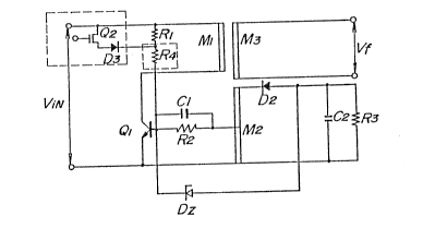
Referring firstly to Figure 1 of the drawlngs,
Q1 denotes a switchlng (oscillation) transistor, R1 and R4
denote star~iny current limi-ting resistors Eor the
switching transistor Q1~ R2 denotes a drive current
limiting transistor, C1 denotes a capacitor for speedin~
up the switching operation of the switching transistor Q1~
D2 denotes a rectifying diode, Dz denotes a Zener diode
~or voltage regulation, C2 denotes a smoothing capacitor,
R3 denotes a dummy load, and M1, M2, and M3 denote colls.
In the present embodiment, there are also
provided a transistor Q2 for selecting the starting
resistance for the switchin~ transistor Q1 and a diode D3
for protecting the transistor Q2
The present converter circuit is intended to
provide an output voltage Vf in response to an input
voltage Vin and the output voltage Vf is determined
virtually by the magnitude of the input voltage Vin and
the ratio of the number of turns of the coil M1 to the
number of turns of the coil M3.
In the present embodiment, it is arranged such
that, when the input voltage Vin is changed, selection is
~2~ 9
made by operation of a part of the circuit enclosed by the
broken line ~Inder control of a control portion (not
shown), and thereby, the startin~ resistance for the
switching transistor Q1 is switched from R4 to R1 + R4.
It is also possible to enable selection among three or
more resistance values by increasing the number of the
resistors.
Referring now to Figure 2, wherein a state in
which, for a given output voltage Vs, the input voltage
Vin is high is indicated by curve A and the state in which
the input voltage Vin is low is indicated by curve ~, in
order to bring the output voltage to one and the same set
value Vs for both the input voltage V1 on the curve A and
the input voltage V2 on the curve B, the starting
resistance determining the operating point of the
switching transistor Ql is selected to be of the value
suited for either one of the above-mentioned states.
More concretely, in the state of the curve A,
the bias of the base of the switching transistor Q1 is
controlled -to become the optimum value by
(R1 + R4) : R2~
and in the state of the curve B, the bias of the switching
translstor Q1 i5 controlled to become the optimum value by
R4 : R2 .
The reason why the input-output characteristics
as shown in Figure 2 are obtained is that, in the state of
the curve B, as compared with the state of the curve A,
the OFF time of the switching transistor Q1 is made
shorter, and also the rise time from OFF to ON is
decreased, and rate of change of current di/dt is thereby
increased, and hence, the induced voltage on the secondary
side in the state of the curve B is increased more than
that in the state of the curve A.
Thus, a constant output voltage Vs is maintained
by using the voltage characteristic of the curve A when
the input voltage is V1 and using the voltage
characteristic of the curve B when the input voltage is
V2 ~
Another embodiment of the invention is shown in
Figure 3. Reference numerals in Figure 3 are equivalent
to those in Figure 1. D1 denotes a diode.
Although the manner of interconnection therein
is different from the previously described embodiment, the
technique to change the starting resistance for the
switching transistor Q1~ and thereby to obtain a fixed
A.C. voltage (set value) on the secondary side from the
input voltages Vin on the primary side is embodled in the
present drawing.
In constructing ~ circuit in practice, of
course, it is preferable to select either the first
embodiment or the second embodiment in accordance with the
merit in actual mounting.
Incidentally, if the starting resistance value
for the switching transistor is changed with the input
voltage kept constant, then two kinds of output A.C.
voltage values are obtained.
As described so far, the conver-ter circuit of
the present invention is provided with an oscillation
transistor and adapted such that a fixed A,C. voltage is
obtained on the secondary side from input vol-tages on the
primary side by changing the star-ting resistance for the
oscillation transistor, and therefore, it is possible to
provide the converter circuit for enabling the A.C. output
voltage at one and the same level to be obtained from the
inp~t voltages at a plurality of points, the converter
circuit being usable with a wide variety of the input
voltages, using a small number of parts and at a low
manufacturing cost,
While only certain embodiments of the present
invention have been described, it will be apparen-t to
those skilled in the art that various changes and
modifications may be made therein without departing from
the spirit and scope of the present invention as claimed,