Note: Descriptions are shown in the official language in which they were submitted.
~3
- 1 -
This invention concerns an image reading device used in
electronic print boards, ~acsimile machines or the like, in
particular a device capable of detecting that a light source
for illuminating a source document is off.
In a conventional image reader of this type, there is a
lamp for lighting a source document, a shad:Lng plate which
smooths the light intensity distribution of a reflected
light from the source document, an image formation lens, and
a line sensor which includes a line of photoelectric
conversion elements for producing an image signal. An
amplifier amplifies the image signal read by the line
sensor to produce an amplified image signal. ~ comparator
compares the ampli-Eied image signal with a slice level to
produce a series of binary pixel signals. A counter counts
the binary signals of a value. There are also a control
circuit, a memory and a D/A converter.
In -this configuration, the image signal produced by the
line sensor is amplified by the amplifier, becoming the
amplified image signal, and is input into the comparator.
The amplified image signal is then converted to binary
signals by way of a comparison with the slice level produced
by the D/A converter.
Prior to the start of actual image reading, the pea}c
value of one line of the image signal is determined and a
threshold level to be used in the subsequent actual image
reading is obtained from the peak value thus determined.
-- 2
This is done in the following manner. For purposes of the
following description, "actual image reading" means the
process of reading data from an area of source document on
which images (characters, symbols, pictures, etc., to be
processed) have been written. The "threshold level" means
the slice level used during actual image reading. As a
first step, the control circuit calls for the maximum value
of the slice level information (these slice levels are used
for finding the peak value of the image signal) stored
earlier in the memory. Control circuit inputs into the
comparator, the slice level information which is converted
at the D/A converter, together with the reference voltage
vcO, into an analog signal of a value of a slice level
stored in memory. Under this condition, the line sensor
reads one line of the image, and the amplified image signal
is input into the comparator. This image signal is compared
with the aforementioned slice level, and is ou~put as binary
signals consisting of "1" and "0" bits. The binary signals
of a value "1" are counted by thé counter, the result of the
counting is then input into the control circuit. When the
count value at the end of reading of each line is less than
a certain value, the control circuit calls from the memory
slice level information, e.g., a level which is one step
lower than the previously called slice level information.
In this way, the control circuit repeats the same operation,
gradually decreasing the slice level information until the
count value becomes equal to or greater than the de~ined
value, Suppose, for example, that a certain slice level is
the largest slice value which gives a count value of not
less than the defined value. Then this slice level is
recognized as the peak level and the control circuit raises
a carry flag, calls from the memory the threshold level X
information corresponding to this peak level, sets X as
threshold level and then performs actual image reading.
In such a conEiguration, when the lamp is not lit or
"off" the carry flag will not be raised by the control
circuit even if the slice level is lowered to the minimum
slice level obtainable from the slice level information
stored in the memory. When this happens, the conventional
system would conclude that the lamp is not lit.
Another example of a conventional system diFfers from
the above system in that it has a peak-hold circuit ~or
holding -the peak value produced by an amplifler, and that it
varies reference voltage input into the D/A converter
according to the output from the peak-hold circuit. This
enables the system to lower the threshold level when the
light emission intensity from the lamp diminishes due to
aging changes or ambient temperature changes. This also
enables the system to set a threshold level consistent with
the level of image signal to enhance the fidelity with which
the source document is read.
The above conventional systems have the following
- 4 -
problems. The first conventional system is capable of
detecting the condition of the lamp not lit. However, if
the light emission intensity of the lamp changes due to the
aging or a decrease in the ambient temperature, since
threshold level remains at a Eixed level, the threshold
level will become inappropriate, resulting in decreased
fidelity of image reading relative to the source do~ument
image.
Also, even though it was possible for the second
conventional system to set a threshold level by taking into
account the light emission intensity from the lamp to ensure
good fidelity reading of images even in the event of a
change in light intensity from the lamp, when the lamp is
not lit, the reference voltage will decrease. When this
happens, the level of the image signal (corresponding to the
dark electric potential level) becomes larger than the
lowest slice level. Under this condition, the conventional
system would fail to detect that the lamp is not lit.
The present invention provides an image reading device
capable of high-fidelity reading of source document images
as well as capable of detecting the not lit or "off"
condition of a light source.
An image reading device for this invention comprises a
light source for illumina~ing a medium to be read, a line
sensor includlng a line of photoelectric conversion elements
for receiving light from the medium and producing an image
~ 5 ~3~
signal, means for determining white levels for respective
intervals into which said line of photoelectric conversion
el.ements are divided, means setting threshold levels Eor the
respective intervals on the basis of said white levels for
the respective intervals, means for comparing the image
signal with said threshold levels to produce a series of
binary signals, and means for dekecting the "off" condition
of the light source on the basis of the r~lative magnitudes
between the white levels for the respective intervals.
In a preferred embodiment, such detection is made on
the basis of the difEerence between the maximum and minimum
values of the white levels for the intervals.
In another preferred embodiment, the detection is made
on the basis of the white levels for the intervals that are
adjacent each other and located in a predefined region.
In the drawings,
Figure 1 is a block diagram showing an example of a
prior art device;
Figures 2A and 2B are graphs showing the relationship
2~ between slice levels for finding the peak value and an image
signal generated from the prior art device of Figure 1;
Figure 3 is a block diagram showing another example of
a prior art devi.ce;
Figures 4A, 4B and 4C are graphs showing the
relationship between reference potentials and an image
signal generated from the prior art device of Figure 3;
~5~6~ ~
-- 6 --
Figure 5 is a block diagram showing an embodiment oE
the invention;
Figures 6A, 6B and 6C are graphs showing -the
relationship between reference potentials, an image signal
and threshold levels;
Figure 7 is a flow chart showing the operation of the
embodiment of Figure 5;
Figure 8 is a block diagram showing another embodiment
of the invention;
Figures 9A, 9B and 9C are graphs showing the
relationship between reference potentials, an image signal
and threshold levels;
Figure 10 is a graph showing a potential reference and
an image signal in a ~urther embodiment of the invention;
and
Figures llA, llB and llC are graphs showing an image
signal in a further embodiment.
A conventional image reader used in electronic print
boards, facsimile machines and the like is shown in block
diagram of Figure 1. In this figure, there is a lamp 1 for
lighting a source document P, a shading plate 2 which
smooths the light intensity distribution of a reflected
light L from the source document P, an image formation lens
3, and a line sensor 4 which includes a line of
photoelectric conversion elements for producing an image
signal A. An amplifier 5 amplifies the image signal read by
Ç~3
- 7 -
line sensor 4 to produce an amplified image signal B. A
comparator 6 compares the amplified image signal B with a
slice level D to produce a series of binary pixel signals.
A counter 7 counts the binary signals of a value "1". There
are also provided a control circuit 8, a memory 9 and a D/A
converter 10.
In the above configuration, the image signal A produced
by line sensor ~ is amplified by amplifier 5, becoming the
amplified i.mage signal B, and is input into the comparator
6. Image signal B is then converted to binary signals F by
way of a comparison with slice level D produced by D/A
converter 10.
Prior to the start of actual image reading, the peak
value of one line of the image signal is determined and a
~ 15 threshold level to be used in the subsequent actual image
reading is obtained from the peak value thus determined.
This is done in the following manner. For purposes of the
following description, "actual image reading" means the
process of reading data from an area of source document on
which images (characters, symbols, pictures, etc., to be
processed) have been written. The "threshold level" mea~s
the slice level D used during actual image reading. Figures
2A and 2s are graphs showing the relationship between the
slice levels and the image signals. As shown in Figure 2A,
as a first step, control circuit 8 calls for the maximum
value of the slice level information ~these slice levels are
t
~ 5~
-- 8
used for finding the peak value of the image signal) stored
earlier in memory ~. Control circuit 8 inputs into
comparator 6 the slice level in-formation E, which is
converted at the D/A converter 10, together with the
reference voltage Vco, in to an analog signal D of a value
of slice level VP1 stored in memory 9. Under this
condition, the line sensor 4 reads one line of the image,
and image signal B is input into the comparator 6. The
image signal B is compared with slice level VP1, and is
ou-tput as binary signals F consis-ting of "1" and "0" bits.
Binary signals F of a value "1" are counted by counter 7,
the result of the counting, G, is then input into control
circuit 8. When the count value G at the end of reading of
each line is less than a certain value, control circuit 8
calls from memory 9 slice level information, e.g., VP2 which
is one step lower than the previously called slice level
information, e.g., VP1. In this way, the control circuit
repeats the same operation, gradually decreasing the slice
level information until the count value G becomes equal to
or greater than the defined value. Suppose, for example,
that the slice level VPj is the largest slice value which
- gives the count value G of not less than the defined value.
Then the slice level ~Pj is recognized as the peak level and
control circuit 8 raises a carry flag, calls from memory 9
the threshold level SLj information corresponding to peak
level VPj, sets SLj as threshold level D and then performs
actual image reading.
In such a configuration, when lamp 1 is not lit or
"off" the carry flag will not be raised by control circuit 8
even if the slice level is lowered to VPm, the minimum slice
level obtainable from the slice level information stored in
memory 9. ~hen this happens, the conventional system would
conclude that lamp 1 is not lit.
Another example of a conventional system is the
configuration shown in the block diagram of Figure 3. The
system in this example differs from that in Figure 1 in that
it has peak-hold circuit 11 for holding the peak value
- produced by amplifier 5, and that it varies reference
voltage VvAR input into D/A converter 10 according to the
output from peak-hold circuit 11. This enables the system
to lower the threshold level when the light emission
intensity from lamp 1 diminishes due to aging changes or
ambient temperature changes. This also enables the system
to set threshold level D consistent with the level of image
signal B to enhance the fidelity with which source document
P is read.
The above conventional systems have the following
problems. The conventional system of Figure 1 is capable of
detecting the condition of lamp 1 not lit. However, if the
light emission intensity of lamp 1 changes due to the aging
or a decrease in the ambient temperature, since threshold
level D remains at a fixed level, threshold level D will
`3~ i3
become inappropriate, resulting in decreased fidelity of
image reading relative to the source document image.
Also, even though it was possible for the conventional
system of Figure 3 to set a threshold level by taking into
account the light emission intensity from lamp 1 to ensure
good fidelity reading of images even in the event of a
change in light intensi-ty from lamp 1, when lamp 1 is not
lit, reEerence voltage VvAR will decrease from the condition
shown in Figure 4A to that shown in Figure 4B. When this
happens, the level of image signal B (corresponding to the
dark electric potential level) becomes larger than the
lowest slice level VPm, as shown in Figure 4C which is an
enlargement of Figure 4B in the direction o-E the signal
; level. Under this condition, the conventional system of
lS Figure 3 would fail to detect that lamp 1 is not lit.
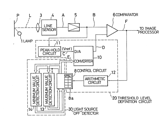
An embodiment of the invention is shown in Figure 5 and
is an image reader used in an electronic print board. As is
customary, the electronic print board of this embodiment
uses a fluorescent lamp 1 as shown in Figure 1 to illuminate
a source documen~ (the medium to be read) which in this
embodiment is a movable screen P on which characters,
symbols and pictures are written. The light reElected from
the movable screen P is focused by an image forming lens 3
on a line image sensor 4 such as a linear CCD (charge-
coupled device) having a line of multiple, e.g., 12~0photoelectric conversion elements by which the optical input
~i ~ 2~5~`3
-- 11 --
is converted into an electric signal A called a video or
image signal. The image signal ~ is compared with a slice
level D to produce a series of binary pixel signals F. The
binary pixei signals F indicate the black or white of
respec-tive pixels during an actual image reading.
The line sensor comprises 1280 photoelectric conversion
elements. This means that -the entire height (the dimension
in the direction parallel to the line) of the screen P
consists in effect of 1280 pixels. The entire line is
evenly divided into n, e.g., 10 sections or intervals and
each section consists of 128 pixels.
As will be described in further detail later, the
highest of the pixel signals (samples of an image signal
corresponding to the respective pixels) within each
interval is regarded as the white level for that interval
and the threshold level for that interval is determined
based on this white level. Here the term "highest" means
"m-th highest" where m is a natural number.
In the example under consideration, m = 10, i.e., the
tenth highest value of the pixel signals in each in-terval is
found to be the white level of the interval. The white
level is represented as a digital value of 7 bits, i.e. of
128 steps.
The line sensor 4 receives reflected light from a
screen (recording medium) P on which letters, symbols and/or
pictures are written, and converts the light into an
`,~'
''' .
- 12
electric signal to produce an image signal A by scanning.
An amplifier 5 amplifies the image signal A to p-roduce
an amplified image signal B, which is input to a peak-hold
circuit 11 and a comparator 6.
Peak-hold circuit 11 holds the peak value of the input
that has been applied to it, and its output C is input to a
reference voltage terminal Vref of a D/A (digital-to-analog)
converter 10 to be used as the reference voltage. Supplied
to the input data terminal of D/A converter 10 is digital
data E from a control circuit 8.
Control circuit 8 has a memory 8a which, similar to
memory 9 shown in Figure 1, stores a table providing
correspondence between the white levels and the threshold
levels. Control circuit 8 calls from the correspondence
table the threshold level information corresponding to the
; white level and transfers threshold level information E to
D/A converter 10.
D/A converter 10 converts the digital slice level or
threshold level information E into an analog slice level
signal D using the output (peak value) from the peak-hold
circuit 11 as the reference voltage Vref.
The output D of D/A converter 10 is supplied to the
comparator 6 as a threshold level D to be used during the
process of the actual image reading. The output D from the
D/~ conver-ter is also used as a slice level during the
process of determi.ning the white level.
5~3
- 13
During the process of determining the white level,
comparator 6 compares the image signal B with the slice
level D to convert -the image signal into a series of binary
(pixel) signals F of "1" or "0" depsnding on whether or not
the image signal B is larger than the slice level D.
The binary signals F are input to arithmetic circuit 12
having func-tions of rnultiple (e.g. 10) counters, which are
se~uentially enabled by the control circuit 8. The counters
are alloted to the respective intervals or sections, and
each counter is enabled when the pixel signals of the
corresponding interval are processed. The control circuit
8, in cooperation with each counter, serves to determine a
white level for each interval as defined by the tenth
highest value of the pixel signals within the corresponding
interval. This is done by the binary search method. More
particularly, the slice level for each interval is initially
set at the middle, i.e., 128/2. Each counter counts the
number of "1" pixels in each interval by being enabled while
the binary signals of that interval are produced. When the
number of the value "1" pixels thus counted is larger than a
predetermined value, 10 (because the tenth highest value of
the pixel signals is being sought), then the slice level is
increased by 128/22: if not, it is decreased by 128/22.
This process is repeated six times. The amount by which the
slice lèvel is increased or decreased is halved each time
the process is repeated, so that at the sixth process, the
~.~2$~3
- 14
amoun-t by which the slice level is increased or decreased is
128/26+1 = 1. The optimum slice level is thus determined
while six lines are scanned. This slice level remaining in
the counter at the end of the binary search is detected and
stored in the control circuit 8, and gives the tenth highest
value of the pixel signals and is used as the white level.
The reason that the first highest value of the pixel signals
is not used as the white level is that there can be noise
associated with the pixel signals which gives rise to an
especially bright spot which should be ignored.
The control circuit 8 multiplies the whi-te level with a
coefficient, typically having a value between 0.65 ancl 0.75,
e.g., 0.7 to produce a threshold level that should be used
during processing of effective data, i.e., data from the
area of which the image is to be read and processed. This
multiplication is implemented by use of the memory 8a in the
form of a table.
During processing of the actual image data, the control
circuit 8 sequentially selects the threshold level
corresponding to the interval at which the pixel signals are
being processed. AS a result of the comparison made at the
comparator 6 using the threshold level D thus provided, a
signal "1" at the output of the comparator 6 signifies white
(or bright) and a signal "0" signifies black (or dark).
Of the components described above, the peak-hold
circuit 11, the D/A converter 10, the arithme-tic circuit 12
- 15
and the control circuit 8 in combination form a threshold ,
level definitlon circuit 20 which sets the threshold levels
to be input into comparator 6 for the actual image reading.
The image reader of this embodiment is further provided
with a maximum value detection circuit 13 which detects the
maximum value of the white levels of all the intervals and
a minimum value detection circuit 14 which detects the
minimum value of the white levels of all the intervals. The
maximum value detection circuit 13 and the minimum value
detection circuit 14 in combination with the control circuit
8 form a llght source "off" detector circuit 30 for lamp 1.
- In this embodiment, lamp "off" detector circuit 30
determines that lamp 1 is not lit by the following process.
During the setting of threshold level D described above, the
white level information is supplied to maximum value
detection circuit 13 and minimum value detection circuit 14.
When the determination of the white levels is completed, the
maximum and the minimum values of the white levels are left
; in the maximum value detection circuit 13 and the minimum
. 20 value detection circuit 14, and control circuit 8 determines
; that lamp 1 is not lit if the difference between the maximum
value of the white levels detected by the maximum value
. detection circuit 13 and the minimum value of the white
levels detected by the minimum value detection circuit 14 is
less than the specified value.
With reference to Figures 6A -to 6C and 7, the following
;3
- 16
describes how the embodiment of the configuration shown in
Figure 5 operates before the start of an actual reading.
ReEerring to Figure 7 ln step 1, a slice level S is set
for the purpose of determininy the white levels for
intervals 1 to n into which the photoelectric conversion
elements of line sensor 4 are divided. This slice level is
identical for all the intervals and is at the middle of the
full range (e.g., 128/2). Step 2 reads one line of an
image, and outputs binary signals F by cletermining whether a
given image signal is "1" or "0", based on slice level D
set a-t the middle value. Then, arithmetic circuit 12 counts
for the intervals 1 to n the number of value "1" bits
present. Step 3 sets i = 1. Step 4 determines for each
interval i whether slice level S lies above or below the
white level of the image signal B. If it i5 determined that
the white level of image signal B is higher than slice level
S, control is transferred to step 5, where, in accordance
with the binary search method described above, a new slice
level S, higher by 128/2X+1, (x = 1, 2...n), is set. On the
other hand, if it is determined that the white level of
image signal B is lower than slice level S, control is
kransferred to step 6, where, in like manner, a new slice
level D, lowered by 128/2X+2, is set. When the setting by
either step 5 or 6 is completed, control is transferred to
step 7, where a determination whether or not i = n is made.
If i = n, the control is transferred to step 8, where the
. .
;3
- 17
increment opera~ion i = i + 1 is carried ou-t. After that,
the control returns to step a, and similar operations are
repeated n times.
If step 7 finds i = n, control is transferred to step
9, where a determination is made as to whether or not a
predefined number (x-7 in the example under consideration)
of lines have been read. If the answer is negative, the
control returns to step 2, and the operations described in
steps 2 through 8 above are performed on intervals 1 to n.
~; 10 When a predefined number x of lines have been read, the
white level setting operation terminates, resulting in white
levels VP, which differ from interval to interval 1 to n, as
shown in Figure 6A.
Next, the control is transferred to step 10, where a
determination is made as to whether the maximum value Dmax
and the minimum value Dmin of the defined white levels set
for intervals 1 to n are at least equal to DEF. When lamp 1
is lit, as shown in Figure 6A, the output value Dmax from
maximum value detection circuit 13 occurs near the centre
where the light intensity is high, and the output value Dmin
from minimum value detection circuit 14 occurs toward the
edges where the light intensity is low.
Consequently, by defining an appropriate value in DEF,
by taking into consideration conditions that prevail when
the lamp is not lit and conditions that prevail when the
lamp is lit, a determination of Dmax - Dmin~ DEF will be
~ $S~
- 18
valid.
If the determination at step 10 is positive, then
control is transferred to step 11, where a level amounting
to 65 to 75% of the white levels VP are called from memory
~a and set as threshold levels D, after which the actual
image reading is per~ormed. When lamp 1 is "off" or not
lit, image signal B, white level VP, and reference voltage
Vref converge in the vicinity of OV, as shown in Figure 6B.
Then, as shown in Figure 6C which is an enlargement of
Figure 6B along the length of signal level, the difference
Dmax - Dmin becomes very small. Conse~uently, the
-- condition Dmax - DminC DEF results and the determination by
step 10 becomes negative. Then control is transferred to
step 12, where the reading process is cancelled, and the
fact that the light source is "off" or not lit is indicated
by means of an indica-tor lamp, not shown, or by other means.
As previously described, the embodiment of Figure 5 has
a configuration where each line of the image read is split
into n intervals, for each interval the white level of an
image signal is detected, threshold level d is set according
to the detected white level, and at the same time the
- difference between the maximum and minimum values of the
detected white levels is determined, to find whether the
light source is lit or not lit. Consequently, as long as
light enters even only one interval of the line sensor, the
system can determine that the light source is lit.
- lg -
; Also, the system has a circuit configuration where
output signals from the peak-hold circuit 11 are input into
the D/A converter 10 as reference voltages, so that even if
there is a variation in the light intensity from the light
source 1 due to aging changes or a change in ambient
temperature, the images of the source document P can be read
; with good fidelity.
It should be noted that although this embodiment is
described as an improvement over the conventional sys-tem
shown in Figure 1 which does not have a shading plate, the
description of this embodiment should not be construed as a
--- limitation of this invention. Accordingly, this invention
is also applicable to systems provided with a shading plate.
As explained above, since under this invention the
device splits each line into n intervals, sets a white level
for each interval, and determines whether or not the light
source is lit on the basis of the difference between the
maximum and minimum values of the white levels detected in
; the n intervals for a line, the device can determine that
the light source is lit, as long as light enters the reading
means even in a single interval. Thus, the device does not
mistake the condition of "not lit" for "lit", and is capable
of accurately determining the condition of "not lit".
Also, since the output signals from the peak-hold
circuit are input into the D/A converter as reference
electric potentials, even if there is variation in the light
:;
,. j
::'
~3
- 20
intensity from the light source due -to the aging changes or
a change in ambient temperature, high-fidelity reading of
the images from the source document is possible.
Figure 8 shows another embodiment oE the invention.
In this embodiment, a control circuit 18 is provided in
place of the control circuit 8 of Figure 5.
The control circuit 18 has the same functions as the
control circuit 8 with regard to determination oE the white
levels for respective intervals and for providing the
threshold levels during an actual image reading.
The control circuit 18 differs from the control circuit
8 in the manner of light source "off" detec-tion.
Specifically, the control circuit 18 performs the light
source "off" detection on the basis of the relative
magnitudes between white levels for the intervals which are
adjacent to each other and located in a predefined region.
For instance, where the pattern of the levels of an image
signal is generally high at the centre and is decreased
toward the edges, the control circuit 18 applies all or
predetermined ones of the following conditions:
(1) (White level for interval 2) ~ (white level
for interval 3) ' ... ~ (white level for interval
J).
(2) (White level for interval K)~ ... (white level
for interval n-2) ~ (white level for interval
'`
5~ 3
- 21
n-l).
. `
(3) The white level for interval 1 is below a
predefined value.
:
(4) The white level for interval n is below a
. ~.
predefined value.
.~,. .
In the above conditionsj intervals 2 through J lie on
the left of the central interval of maximum light intensity,
intervals K through n-l lie on the right of it, and
intervals 1 and n are the intervals with no light input.
The term "predefined value" in condi-tions (3) and (4)
are so set as to be exceeded if any significant amount of
lighk is input during that interval.
Control circuit 18 determines that the light source is
"lit" if the applied conditions are all true, and "not lit"
or "off" if any of the conditions is false.
Figure 9A shows the white levels VP obtained by the
above series of operations when the light source is lit;
image signal B; and reference voltage Vref of D/A converter
10, output from peak-hold circuit 11.
In-tervals 2 through n-l receive light when the light
source remains lit; intervals 1 and n receive no light. The
white level detected for the intervals 1 and n are about the
; same as the dark output level of image signal B.
' ,'
~.."
"'
.. . ... ..
- 22
Based on the white level of image signal B determined
for each interval, control circuit 18 sets threshold level
D, which is analogous to white level VP of image signal B by
reference to a correspondence table similar to that in
memory 8a of Figure 5, and starts an actual reading.
Because no shading plate is employed in the follow-up-
type binarization circuit described, the output signals from
; the image signal B, obtained with the light source lit,
reflect characteristics of the light source and lens,
; 10 forming a pattern in which light intensity is high at the
centre and decreases toward the edges. ~n example of this
effect is illustrated as the image signal B in Figure 9A.
When the follow-up-type binarization circuit is
operated on an image signal B with the light source lit, the
white levels VP representing the m-th highest pixel signals
in respective intervals show a pattern which is high at the
centre and decreasing toward the right and the left. Figure
9A shows an example of the white levels VP.
By contrast, the white levels VP of image signal B
obtained with the light source not lit represent dark output
levels having a very low voltage and form a generally flat
pattern with the effects of noise. When the flat image
signal B is input into peak-hold circuit 11, this circuit
outputs a voltage approximately equal to the white levels VP
of image signal B; this output, then, is input as reference
: voltage Vref of D/A converter 10.
- 23
Control circuit 18 searches for the white levels VP of
image signal B between the reference voltage Vref and zero
volts, and sets threshold levels D or Vp.
Figure 9B shows reference voltage Vref, image signal B
and white levels VP reflecting the condition of the light
source which is not lit or "off". Figure 9C is an
enlargement of the voltage between reference voltage Vref
and zero volts.
Although in Figure 9C, image signal B is shown as a
straight line, in actuality it fluctuates up and down due to
noise and other effec-ts. Peak-hold circuit 11 holds the
- maximum value of the image signal B as it fluctuates up and
down.
The follow-up-type binarization circuit detects the
white levels VP of image signal B for the respective
intervals. As shown in Figure 9C, white levels thus
detected undergo random variations from one interval to
another due to effects of random noise.
As stated earlier, when the light source is lit, white
levels VP for the intervals at the centre are high and are
decreased toward the edges, as illustrated in Figure 9A.
When the light source is not lit, white levels VP have
random magnitudes with no interrelationship between
intervals, as shown in Figure 9B and Figure 9C. Thus, the
condition of the light source which is lit and that of the
light source which is not lit or "off" differ significantly
'';
350Ç~3
- 24
in terms of the patterns of detected white levels VP.
; With the light source lit, the detected white levels of
the intervals not receiving light are the dark output
levels shown for intervals 1 and n in Figure 9~. Such dark
output levels are considerably lower than the reference
voltage Vref output from the peak-hold circuit, i.e., the
detectable maximum level. When the light source is not lit,
reference voltage Vref output from the peak-hold circuit
with the light source ofE is about the same as image signal
B which has become a dark output level, so that the level
for intervals 1 and n may not be detected as a low level.
-- For each image signal B obtained after the start of a
reading but before the start of an actual data reading,
control circuit 18 detects a white level for each interval.
It reduces the white levels with a certain ratio from the
detected white levels to determine threshold levels D
analogous to white levels VP. When it finishes detecting
the white levels of image signal B for the respective
intervals, control circuit 18 uses the following conditions:
(1) (White level for interval 2)~ (white level for
interval 3)G .. 4 white level for interval J).
.
(2) (White level for interval K)> ...~ (white
level for interval n-2)~ (white level for interval
n-1).
:
~ ~35~
- 25
(3) The white level for interval 1 is below a
predefined value.
(~) The white level for interval n is below a
predefined value.
In the above condi-tions, intervals 2 through J lie to
the left of the central interval of maximum light intensity,
intervals K through n-1 lie to the right of it, and
intervals 1 and n are intervals receiving no light input.
The predefined values in the conditions (3) and (~)
are chosen to be exceeded when any significant amount of
light enters these intervals. That is, the predefined
values in conditions (3) and (~) are chosen so as to be
exceeded when the light source is off and not exceeded when
the light source is on. It is possible to set the
; predefined value in this way because the white levels in the
digital values of sections 1 and n become larger when the
;; light source is off. This is because the difference in the
brightness between sections 1 and n at both ends of the line
sensor and the sections in the centre is eliminated when the
light source is off, while such difference is larger when
~, the light source is on.
Control circuit 18 applies either all of the above
conditions or previously specified ones of the above
conditions to the white levels detected for the intervals;
; .
63
- 26
it determines -that the light source is "lit" if the applied
conditions are all true, and "not lit" if any one of the
conditions is false.
In the above embodiment, the comparison of the levels
between intervals was made in terms of a strict inequality.
However, for the intervals in the vicinity of the centre of
an image signal or in situations where, due to the
particular characteristic of the light source, there is not
much difference in light intensity between the centre and
the edges, the conditions "greater than or equal" or "less
than or equal" can be substituted.
Further, although in the above embodiment a line is
divided inko several intervals, as shown in Figure 10, an
interval can be set up for the region of no light~ Then,
given a detected white level, a condition similar to
condition (3) or (4) "with a detected white level less than
or equal to a specified level" can be applied to obtain
similar results. If the "specified level", with which the
detected white level is compared, is varied in proportion to
the reference level Vref, (i.e., the peak level over the
entire line), such variations on the basis of the
conditions (3) and (~) is considered a form of judgment on
the basis of the relative magnitude of the white levels
between the intervals.
In the event that the light a~is in the optical system
gets physically distorted, and if the normal image signal
~35~3
- 27
; shown with dotted lines in Figures 11~, llB and llC take an
abnormal wave pattern, as shown with the solid line, by
applying either condition (1) or (2), or both, the device
can detect that the signals are not normal image signals.
As an alternative to the previous embodiment employing
follow-up-type binarization circuit, the reference voltage
Vref of the D/A conver-ter shown in Figure 8 may be held
constant. Yet, it can be detected that the light source is
not lit, by applying the conditions (1) and (2).
The invention is featured in that the condition of the
light source not lit is detected on the basis of the white
-- levels of the image signal for the respective intervals. In
the various embodiments described, the white levels are
utilized directly for this purpose, i.e., without
intervening processing. But instead the invention is not
limited to such a situation but should be construed to cover
such a situation where the white levels are converted into
corresponding values, which are then utilized for the
detection of a light source "off" condition. For instance,
the threshold levels for the respective intervals which are
determined on the basis of the respective white levels may
be used for the detection of the light source "off"
condition.
The embodiment described eliminates the need for
incorporating into the device photosensors and other
dedicated components for detecting the light source "off"
,
., ~
~ (5~5~
. .
- 28
condition, and makes it pos,sible to detect the light source
"off" condition through the use of a binarization circuit.
Also, by entering output signals from the peak-hold
circuit as a reference voltage for the DJA converter, the
device is capable of detecting the light source "off"
condition unaffected by changes in light intensity from the
~ light source due to aging changes or a temperature
: variation.
.' .
.