Note: Descriptions are shown in the official language in which they were submitted.
7qL
- 1 - 25307-169
The present invention relates to a data error detection
circuit to be used for a data transmission system in which low
speed data is transmitted through a high speed -transmission line
by repeating transmission of the low speed data a plurality of
times.
A variety of systems have been proposed for trans-
mitting low speed data through a high speed transmission line.
The high speed universal transmission system is a typical system
wherein the low speed data is transmitted by repeating a plurality
of times transmission of the low speed data.
More particularly, in such a high speed universal
transmission system, a plurality of low speed data bits are
gathered in the form of a low speed frame and such low speed frame
is transmitted a plurality of times.
The background of the invention will be described in
greater detail with reference to the accompanying drawings, in
which:
Figure l indicates a frame format for transmission of
low speed data by a high speed universal data transmission
system;
Figure 2 is a block diagram of an error detection
circuit and an error correction circuit of a preferred embodiment
of the present invention; and
Figure 3 indicates respective output data in Figure 2.
Figure l is an ordinary frame format in a high speed
universal transmission system. The low speed data switches the
-- 2 - 25307-169
data at the timing of the rising edge of the low speed data clock.
In the example oE Figure 1, a total of six low speed data bits
Do-D5 which are continuous in time are gathered to form a low speed
frame. The low speed frame is given the frame bit F which
indicates the leading end of the frame and the bit S which indicates
the trailing end of the frame. Therefore, one low speed frame is
formed by 8 bits of low speed data.
A high speed universal data is formed by repetition of
a plurality of times of such low speed frame. The number of times
of repetition of the low speed frame is determined by the speed
ratio between the low speed data clock and the high speed data clock.
In the case of Figure 1, since the high speed data clock is 5 times
the speed of the low speed data clock, the high speed universal data
is formed by repeating 5 times the low speed frame. Accordingly,
the high speed universal data I-V is obtained by repetition of
the same low speed frame.
The high speed universal data is used, for example,
to convert low speed subscriber line transmission to high speed
transmission.
In the case of transmitting the low speed data using
the frame format of the high speed universal transmission system
of Figure 1, only the high speed universal data is received at the
receiving side. The high speed frarne clock may be recovered from
the frame bits included in the received high speed universal data
but this universal data does not include the information about the
number of times of repetition of the low speed data. Therefore, the
~ ~LZ~5~7~
- 3 - 25307-169
timing of partition for repeated data cannot be defined and it is
difficult when data content has changed to discriminate whether
such change results from partition in the repetition of the data
or from data error.
It is an object of the present invention to provide a
data error detection circuit which can detect data error by dis-
criminating whether any change of content of high speed universal
data results from partition in the repetition of the data or from
data error, without inclusion of information about the number of
times the low speed data is repeated to obtain the high speed
universal data.
It is another object of the present invention to
provide a circuit which can correct the data error au-tomatically
with a simplified circuit structure.
In the present invention, the high speed universal
data is converted to parallel data from serial data and the
parallel signal at the same positions of the high speed frame is
extracted. Continuously, it is detected whether this parallel
signal totally includes the same data or not sequentially. If the
parallel signal including different data continues for the number
of times wnder the specified times, it is discriminated as
partition by repetition of data and if such parallel signal con-
tinues exceeding the specified number of times, it is discrimin-
ated as data error.
In addition, if said parallel signal includes
different data in the present invention, data error is automatically
- .
7~
25307-169
corrected only by holding the just preceding data.
According to one aspect, the invention provides a data
error detection circuit for de~ecting a data error and a data
partition in high speed data, comprising: input means, for
receivinq high speed serial data including high speed data frames,
each high speed da~a frame corresponding to a number of
repetitions of a low speed data frame, and the high speed serial
data does not include information related to the number of
repetitions of the low speed data frame; serial/parallel
conversion means, for conver~ing ~he high speed serial data into n
bits of parallel output data corresponding to specific bits from n
of the hiyh speed data frames, where n is an integer having a
value greater than 1 and less than ~he number of repetitions;
coincidence detection means, operatively connected to said
serial/parallel conversion means, for detecting coincidence and
noncoincidence of individual bits of said parallel output data
from said serial/parallel conversion means, for providing outputs
of data hits co~responding to the coincidence and noncoincidence
of said parallel output data, and for de~ecting the data partition
when a number of consecutive noncoincidences of said parallel
: output data detected is n-1; and error detection means,
operatively connected to said coincidence detection means, for
detecting the data error and providing a data error output signal
when the number of consecutive noncoincidences of said parallel
output data is at least n.
According to another aspect, the invention provides a
method for detecting a data partition in high speed universal
,,
,
7`~
25307-lG9
serial da~a to produce serial ou~put data, comprising: (a)
receiving the high speed universal serial data, the high speed
unirersal serial data includes high speed data frames, each high
speed data frame corresponding to a number of repetitions of a low
speed da~a frame; (b) converting the high speed universal serial
data into n bits of parallel output data corresponding to n of the
high speed data frames, where n is an integer having a value
greater than 1 and less than the number of repetitions; (c)
detecting the data partition when a number of consecutive
noncoincidences of the parallel output data is n-1; and Id) pro-
ducing the serial output data in accordance with the number of
consecutive noncoincidences of the parallel output data.
The invention will now ba describecl in greater detail
with reference to the drawings.
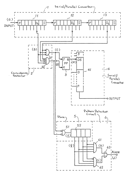
The preferred embodiment of the present invention will
now be explained with reference to Figure 2 and Figure 3. Figure
2 is a block diagram of the embodiment of the invention, while
Figure 3 illustrates output data o~ various parts of Figure 2.
Specifically, locations (a)-lj) in Figure 2 correspond to (a)-(j)
in Figure 3. The high speed universal data (INPUT) is input to a
serial/parallel conversion circuit 1 and then output as a parallel
signal. The serial/parallel conversion circuit 1 can obtain the
period of hiyh speed frame by receiving the frame bit and
extracting the bits in the same positional relation as the
parallel signal. The serial/parallel conversion circuit 1
includes, for example, shift registers 11, 12, 13 connected in
series. The fifth data D5 1' D5 2' D5_3, ... which are given the
4a
,. . .
25307-16g
mark on the bits are output from the high speed universal data as
shown in Figure 3(a). Figure 3~b) shows the signal where the data
bits sequentially output from the serialiparallel conversion
circuit 1 are arranged on a time series bas:is. As in the case of
the signal of Figure 1, the same data is repeated in every 5 bits
and is output as the high speed universal data. In the example of
Figure 3(b), the first data is "O" and subseguently "1", "1", "O"
are transmitted. However, it is supposed here that an error is
generated at the second bit of the third data "1" as indicated by
an asterisk.
4b
, .
:
" -
_ 5 _ 25307-169
As explained previously, the serial/parallel con-
version circuit 1 is formed by connecting in series three shift
registers 11, 12 and 13. Therefore, the parallel signal of three
bits therefrom are extracted, as indicated at the lower side of
Figure 3(b), by sequentially shiEting bit by bit the output of
Figure 3(b) in every three bits.
An output of the serial/parallel conversion circuit
1 is input to the coincidence detection circuit 2 which detects
whether the parallel signal of said three bits includes the same
data or not. The coincidence detection circuit 2 comprises an AND
circuit 21 and an AND circuit 22 with input inversion terminals
which are arranged in parallel. The AND circuit 21 and AND circuit
22 allow input of the output of said serial/parallel conversion
circuit 1. Since the serial/paralle] conversion circuit 1 pro-
vides an output of 3 bits of data, the AND circuit 21 and 22 each
have three input terminals.
An output of the AND terminal 21 for the input
signal indicated in Figure 3(b) is shown as Figure 3tc)l while an
output of the AND circuit 22 is shown as Figure 3(d).
As will be apparent from Figure 3, when the input
signal is all "0", the output of the AND circuit 21 becomes "0"
and the output of the AND circuit 22 with input inversion terminal
becomes "1". In the same way, when the input signal is all "1",
the output of the AND circuit 21 becomes "1" and the output of the
AND circuit 22 becomes "0". Namely, when input parallel signals of
the three bits are all equal, "1" is output from either one of the
.2~35~
- 6 - 25307-169
two output terminals of the coincidence detection circuit 2.
On the other hand, when "1" and "0" are simultan-
eously present at the three parallel input terminals of AND circuit
21, the output becomes "0". Similarly, when thereare both "1" and
"0" at the input terminals of AND circuit 22 its output becomes "0".
As described previously, in the case where the
parallel input signals coincide in the coincidence detection
circuit 2, "1" is output from one of the outputs (c) or (d) de-
pending on the kind of data coincided, while in the case where the
parallel input signals do no-t coincide, "0" is output from both
outputs (c) and (d) as shown in E`igure 3.
The present invention, (1) discriminates partition
of repeated data and data error by utilizing an output of the coin-
cidence detection circuit 2 and accurately detects data error, and
(2) automatically corrects such data error.
The structure for detection of data error is first
explained hereunder.
A store circuit 5 and a pattern detection circuit 6
indicated in Figure 2 are used for data error detection.
As indicated in Figures 3(c), (d), when outputs of
serial/parallel conversion circuit 1 do not all coincide, both
outputs of the coincidence detection circuit 2 become "0". How-
ever, it is impossible to de-tect data error only with output of this
coincidence detection circuit 2. That is because at the partition
between each pair of consecutive bits, indicated as 23 for example
in Figure 3(b), the lack of coincidence could be due not to data/
` ~ 2~35~7~
- 7 - 25307-169
error but simply becomes the bits on either side of the partition
are different.
However, as illustrated at the lower part of
Figure 3(b), non-coincidence of the parallel bits at the partition
in repetition of data continues only for two bits. On the other
hand, when data error is generated, non-coincidence continues more
than two bits.
Therefore, partition in repetition of aata and data
error can be discriminated depending on how long non-coincidence
of -the parallel signal of three bits continues.
In general, when the parallel output signals of n-
bit are extracted, non-coincidence of data is generatecl for the
(n-l) bits in the case of partition in repetition of data or n-bits
or more in the case of data error. In the case of the embodiment
shown in Figure 2 and Figure 3, -the parallel outpu-t signals of
three bits are extracted and therefore da-ta error can be detected
by continuous non-coincidence of parallel data of three times.
In the embodiment shown in Figure 2, the AND circuit
Sl with input inversion terminal provided to the store means S
first detects non-coincidence of parallel data of three bits. The
AND circuit 51 outputs "1" when both outputs (c) and (d) of the
coincidence detection circuit 2 are "0", namely the parallel
signals do not coincide. The output of this AND circuit 51 pro-
vides two continuous "1" for the partition in repetition of data
or three continuous "1" for data error as indicated in Figure 3(f).
The output of this AND circuit 51 is then input to
~ 2~5~3~4
- 8 - 25307-169
a four bit shift register 52, having the function of detecting on
a tlme series basis the output of the AND circuit 51. As shown in
Figure 3(g), an output every 4-bits is provided while it is shifted
bit by bit.
The output of shift register 52 is then input to the
pattern detection cireuit 6. This pattern detection circuit 6
comprises a AND circuit 61 having 4 input terminals, a 4-input AND
cireuit 62 of whieh only one input terminal is inverted and an OR
circuit 63 which obtains the logieal sum of outputs of the AND
circuits 61 and 62. The AND circuit 62 outputs "1" when "1" is
continued for three times as the ouput from the shift register 52
(Figure 3(i)), while the AND cireuit 61 outputs "1" when "1" is
eontinued more than three times as the output from the shift register
52 (Figure 3(h)). The OR eircuit 63 outputs an alarm (Figure 3(j))
when either output of the AND circuits 61 and 62 becomes "1"~
As explained previously, it is possible in the present
invention to detect non-eoincidence in repetition of data, namely
to detect that "1" is continued for the specified times (three
tirnes) or more in the output of AND circuit 51. Therefore, data
error may also be detected by a counter circuit such as an up/down
counter, etc. However, in the case of the embodiment shown in
Figure 2, the circuit may be constituted in a simple fashion by the
shift register and AND circuits.
In the pattern detection means 6, 4-input AND
circuits are used for the AND circuits 61, 62, the AND circuit 61
being provided for detecting four times of con-tinuous "1", whereby
~2~
- 9 - 25307-169
the OR output is used as the alarm signal in order to detect
continuous data bits error of two bits. Such an arrangement
improves reliability of data error detection.
For the same reason as described above, coincidence
of parallel data of three bits is detected in Figure 2 and Figure 3.
Namely, according to the principle of the present invention, data
error may also be detected by using shift registers of two stages
in the serial/parallel conversion circuit to obtain the parallel
signal of two bits and by detecting coincidence of such parallel
signal. However, in the parallel signal of two bits, since con-
tinuous two data bits errors and partition in repetition of data
cannot be discriminated, the parallel output of three bits is
obtained in the embodiment of Figure 2.
For the reason described above, the greater the
number of parallel signals from the serial/parallel conversion
circuit, the more the capability of discriminating continuous data
error is improved.
However, more parallel bits from the serial/parallel
conversion circuit results in an increase of the number of stages
of the shift register used in such serial/parallel conversion
circuit ana therby complicating the circuit structure. Accordingly,
the use of three bits is considered optimum from the point of view
of reliability in data error detection and cost/size of device.
Correction of data error is carried out by holding
the immediately preceding data in the case where non-coincidence
of data is detected in the coincidence detection circuit 2. As
5~
- 10 - 25307-169
such data holding circuit, a J-K flip-flop 3 is used in the
embodiment of Figure 2. The J-K flip-flop 3 outputs a value of
data input to the J input terminal in the case where the input data
to the J-K input terminals are different and holds a value of the
immediately preceding output in case both inputs to the J-K input
terminals are "0".
By referring to Figures 3(c), (d), (e),
i) When (c) = "0", ~d) = "1", the parallel signal of three
bits from the serial/parallel conversion circuit 1 coincide as "0".
Since the inputs -to the J-K flip-flop 3 are "0" and "1" for
respective J-K input terminals, the Q output (e) from the J-K flip-
flop 3 becomes "0".
ii) When (c) = "1", (d) = "0", the parallel signal of three
bits from the serial/parallel conversion circuit 1 coincide as "1".
Since the inputs to the J-K flip-flop 3 are "1", "0", the Q output
(e) from the J-K flip-flop 3 becomes "l".
iii) When (c) = "0", (d) = "0", the parallel signal of three
bits from the serial/parallel conversion circuit 1 do not coincide.
Since both inputs to the J-K flip-flop 3 become "0", the Q output
(e) of the J-K flip-flop 3 holds the jus-t preceding output state.
As explained previously, the J-K flip-flop 3 outputs
the data the same as the input data or a value the same as the
just preceding output data depending on coincidence/non-coincidence
of the input parallel signal.
The output of flip-flop 3 is converted to serial data
by a shift register 41 provided in a serial/parallel converter 4
~ 25307-169
and is then output.
As will be understood from comparison between the
output of J-K flip-flop 3 shown in Figure 3(e) and the input data
shown in Figure 3(b), the J-K flip-flop 3 holds the just preceding
data wi-thout discriminating the partition in repetition of data or
data error in the case where outputs from the parallel/serial
conversion circuit 1 do not coincide. Thereby, correspondence
between input and output is delayed 2-bit by 2-bit but data error
can be corrected.
As described previously, according to the present
invention, partition in repetition of data and data error may be
discriminated without insertion of low speed frame or information
such as the number of times of repetition of low speed data into
the high speed universal data. In addition, data error of high
speed universal data may be corrected automatically using only a
very simpliEied structure.
Here, error must be detected in parallel with error
correction because generation of error in the data must be
recognized by a supervisor and execution of error correction must
also simultaneously be informed to the external circuit.