Note: Descriptions are shown in the official language in which they were submitted.
. ~
BACRGROUND OF THE INVEM ION
1. Field of the Invent~on:
The present invention relates generally to novel
data storage systems and particularly to direct memory access
techniques for storing serial point to point digital encoded
data,
2. Description of the Prior ~rt:
Multichannel digital data acquisition systems which
require transferring data from illustratively a hostile
environment to a less hostile environment must have means for
transferring ~he multichannels of data. ~Jhen many channels
of data are eequired, for example, sixty four channels of
data, and if the digital data to be transferred is parallel
data~ having a word size illustratively of 16 ~its, then 16 x
64 or 1024 separate parallel lines would be necessar~O
To convert the sixty-four channels of parallel data
to serial data and then transfer the data to a remote
location, reconstruct the data to parallel words and then
store the parallel words, presents problems with respect to
coordination and circuit noise which could distort the
transferred data.
A search was made for means of transferring a
series of digital data words representations rom one point
2 ~ S~
to an~ther and then into ~t~rage 1~ memory ~t a rate faster
than the sampled rate used to Ecan the mult~channels wh~ch
w~uld not dist~rt the transferred data due to noise and other
con~ideration such as s~ze. The ~earch resulted in the
serial data direct memory access system o.E the present
invention~
SUMMARY
A direct memory access system which handles point
to point transfer of serial data of serial data from
multichannel acqui~ition systems. The multichannel systems
may be the type which convert an analog signal from
multichannel inputs and convert each channel data into
parallel diyital data at a specific rate. ~his parallel data
is converted to serial data in order to apply the principles
of this invention. The apparatus of this invention includes
a receiver circuit which accepts serial data clocked a~ a
chosen rate. Within the receiver circuit are means for
converting the incoming serial data to parallel data at the
chosen clock rates. Means are also provided for forming and
assigning addresses to each data word that is inputted.
. ~
The apparatus also includes a computer controlled
bus system with expandable memory. The bus system computer
operates at a higher clock rate than the rate of the incoming
data. However, the bus system computer shares control o~
accessing memory with the receiver circuit.
The receiver circuit provides a means for
transferriny the converted parallel data to the assigned
3.~
address locations of memory in the bus system. When the
receiver circuit is accessing memory the bus system computer
goes to sleep.
Specifically, the invention relates to a serial data
direct memory access system for storing inputted digital
signals in a chosen serial form and clocked at a
predetermined rate into selectable address locations of a
memory, the inputted signals being representations of a
series of digital data words of a chosen word size, a start
lo bit and status code bit which provides identifying
information of each data word. The system comprises. a) a
memory storage computer bus system, the bus system including
a master computer for the bus system and static and dynamic
memories, location of memory space in the memories being
addressable; b) a digital receiver comprised of: 1) means
for converting each inputted clocked digital signal from its
chosen ~ormat into a serial digital data word that it
represents; the conversion occurring at the same clock
frequency of the inputted clocked signal; 2) means for
sequentially shifting each bit of the serial digital data
word onto parallel output lines at same clock rate of the
input signal to form a corresponding parallel digital data
word; 3) means for decoding each status code of each
parallel data word so as to provide an indication of the
status of each data word; 4) means for forming an address
word for each data word, the address word forming being in
response to the status of the decoded status code associated
with each data word; 5) means for transferring control of
the memory storage computer bus system from the bus computer
rn/ ~
35~7~
3a
to the digital receiver; and 6) means for writing each data
word from the digital receiver to the bus system memories
and into the memory locations corresponding to the location
designated by each formed address word, the writing being at
a predetermined writing rate higher than the inputted lock
signal rate.
90lf~c8rwl~7loN OF THE DRAWING
The accompanying drawing, which is incorporated in
and constitutes a part of this specification, illustrates a
preferred embodiment of the invention and, together with the
description, serves to explain the principles of the
invention.
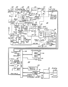
Figure 1 is a block diagrammatic view of a preferred
embodiment of the serial data direct memory access system.
DESCRIPTION OF THE PREFERRED ~MBODIMENT
Referring to Figure 1, there is shown the serial
data direct memory access module 22 of this invention.
Illustratively, serial data in the form of digital light
signals transferring over a fiber optic cable 24 to module
22 enter memory module 22 through the optic receiver 100.
the transferred data includes, illustratively, clock 12 bit
data and 4 bit code information arranged in manchester code
format. The clock rate is illustratively 12 MHz. Module 22
may be configured to accept other data transmission codes
such as nonreturn-to-zero (NRZ) and NRZ-inverted.
Other serial transmission media may be used instead
of optical light signals.
rn/ ~
7 ~ '
Memory module 22 ~nclude~ a recelver circult 90
that includes ~eans for direct memory acce~s to a static or 8
dynamic memory 154 and 152, respect1vely, via a VME bus 130
of a VME bus computer system 133. VME bus system 133
includes the VME bus 130O microcomputer lSS and dynamic and
static memories 152 and 154, respectively. Receiver 100
converts the light signals sent through cable 24 to digital
electrical signals. Cable 24 illustratively is a signal
graded index glass fiber core cable such as a ruggedized type
HFBR-3200 5implex Fiber Optics Cable of ~ewlett-Packard.
The digitized signal is applied to the manchester
decoder 102. Decoder 102 regenerates a synchronous clock
signal and serial bit representation of the data words
transferred to both a start bit counter 104 and serial to
parallel shift register 106. Counter 104 is used to count
the bits looking for a start bit and to latch in the
succeeding 16 data bits.
At ~he 17th clock pulse Q5 of counter 104, a NLOAD~
signal issues which causes the serial data to enter the shift
register 106 and to be clocked by the decoded clock signals.
Shift register 106 reconverts the serial words
representations oE the input data into parallel words
comprised of illustratively 12 data bits and 4 code bits, one
of the code bits being, for example, ~BANK" bit. The three
code bits which define the status of the 12 bit data word is
bussed to decoder/demultiplexer 108. The "BANK" bit is
bussed to decode latch 110 where it is used to clock latch
110 so as to generate a signal to enable decoder 108. When
decoder 108 is enabled the 3-bit code is decoded and either
~ 5
one of the seven circuit~ lndlcator circuits 1R aCt1Yated~
illustrat~vely FAULT l~tch 112, PRECOND ~at~h 114, EVENT
indicator 116, P~E CAL Latch 118, CAL 1ndicator 120; POST CAL
Latch 122 and D~A Latch 124.
The LO~D signal is also used to clock a sequencer
latch 126 so as to enable sequencer 128. Sequencer 128
counts a 16 MHz clock fre~uency signals from a VME bus clock
generator 132 for computer 156. Computer 156 is the master
computer for the bus system.
.1'
The first CLOCK pulse (Ql) is a RESET-l signal
which clears roll latch 134. Roll latch 134 is used to
indicate when memory is full and the system must roll back to
the beginniny. Latch 134 stays clear until memory full
occurs. RESET-l also is used to set decode latch 110 to
begin sequence of decoding the next code bits for the next
data ~ord. The second clock pul~e lQ2) clocks the write
latch 136 which provides a CH ADV signal which enables CH
ADDRESS counter 138 and ~ME counter 139.
. ~'
Counter 138 counts out and its last clock pulse .
enables scan address counter 140. The combined output pulses
from counters 138 and 140 are bussed to address buffer 142 to
form a 16-bit address of the memory location for the data
word that is to be placed in memory. Address buffer 142
transfers the 16-bit address into the address bus of the VME
bus 130 under the command of a TRI-STATE signal issued from
DMA Latch 124.
When scan address counter 140 advances to its last
counter, the final clock pulse is used to enable a
- 5 -
~ :1.29S1~7~3 ~
presettable ~OCR address up~down counter 144 used to
identify which block ~f memory the newly addressed data will
be ~laced in. Illustratively, the amount of data memory i6
expressed in terms of blocks. A block 1~ defined as 2048
words (4096 bytes) of memory for one 51) channel.
Illustratively, f~r 32 channels of lnput data, one ~1) block
would amount to 2048 x 32 or 65~3S words tl31072 bytesl Of
memory. The digital number from counter 144 identifying
which block of memory is to be used i5 bussed to block buffer
146 and then on to the address bus of the VME bus 130 under
Tri-State command~
The pre-condition code latch 114 is used to help
make memory module 22 more noise resistant. ~ precondition
bit is issued with PRECAL, POST CAL and DMA commands to
preve~t spurious signals from entering these circuits.
The addresses generated by the receiver circuit 90
are used to address module 156, dynamic ~AM memory 152 and
; static ~AM memory 154~ These memories can be increased in
size or decreased in size, The static ~AM memory 1~4 is used
as data memory and can be used with a battery back-up for
data retention~ Dynamic RAM memory 152 provides onboard
refresh logicO
There are, illustratively 16 megabytes of address
space of memory but only 6 megabytes are reserved for data
memory starting at for example $800000. The amount of memory
to be used can be varied. ~ maximum memory switch 148 can be
set for the amount of memory installed. Selections are
provided for, illustratively, .5, 1, 2, 4 and 6 megabytes of
78
lnstalled memory. ~he ~wltche ~ust not be ~et for more
memory than ~ ~nstalled, ~lth~gh they coul~ be ~et f~r le~
than rhe installed amount of mem~ry.
As mentioned supra, WRITE latch 136 provides a CH
ADV signal, when the ~econd clock pulse ~Q2) from sequencer
128 changes from a high to a low level. When~
illustratively, a CH ADY signal occurs, VME counter 139 is
~nabled. With latch 136 set as a result of the Q2 clock
pulse, the VME buffer 158 is activated initiating a WRITE
pulse. Then the ~ME bus computer system 130 communicates its
own signals over the bus to the receiver circuit such as
lACR-interrupt acknowled~e, DACR-data acknowledge, AS-ADDRESS
strobe, SYS CLK - System clock. If a ~ACK is not received F
from the bus computer system 130 at the fifth clock pulse ,r
(Q53 from VME counter 139 t this Q5 pulse will be used to
generate a reset signal to reset latch 136. Latch 136 is
essentially used to initiate writing to memory. When the
fifth clock pulse (Q5) of counter 139 occurs, the DAM latch
124 sets providing a T-state or ~ri-state s;gnal for the
system and a LOCR signal to return control back to the CPU of
MC 1560
The data word from shift register 106 is bussed to
auto buffer 160 and then onto the data bus of the VME bus
130. To permit modifying an address, an address modifier
buffer 163 under control of the tri-state signal is used.
DM~ ACCESS
For DMA circuits of memory module 22 to grasp
control of the bus, a form of bus arbitration is employed. A
code from decoder lU8 is issued to the CPV of MC 156
requesting u~e of the bu~. The DMA c~rcults walt for a
response fro~ the CPU. The CPU finishes what it iB do~ng
then it gives up control and goes to sleep. The DMA circu~ts
send a signal to the bus that it has control. When control
is returned to the CPU, the CPV resumes its function from
where it left off prior to go~ng to sleep.
A direct memory access (~MA) ~s in effect whenever
the DMA indicator 150 is lit. This occurs, illustratively,
when coded bits are transmitted to memory module 22,
illustratively, via fiber optic cable 24 indicating the
status of each ~ord. ~llustratively~ a c~de may be sent to
indicate pre cal data, event data, p~st event data, post cal
data. Upon completion of a chosen period of data collecting,
further transmission is stopped. IllustratiYely~ at the end
of post-cal data transmissions, the receiver will ~ive up
control of the system and return control to the CP~ of the
~ME bus.
operation of the system will now be described.
Provided suitable power is applied to module 22, each data
word, illustratively, 16 bits preceaed by a start bit, is
received by memory module 22 via fiber optics cable 24. The
memory module includes circuits which convert the serial data
into a series of parallel 17 bit words, (16 bits and a start
bit).
The optic receiver 100 converts the light signal
to a manchester encoded signal. The manchester decoder 102,
decodes the signal into serial data and a 12 MHz clock pulse.
After a start pulse is detected by start bit counter 104,
serial t~ parallel shift register 106 reconverts the serial
data into parallel words. A decoder 108 decvdes the 3-bit
~tatu~ code to provide ~ndicatlon~ of the type da~a belng
received .
Operating of f a 16 MHz clc>ck pulse from V~E bus
c~mputer system 130, sequencer 128 act~vates several
counters, namely, the VME bus counter 139, a channel address
counter 138, and scan address counter 140, a "BLOCK~ counter
14~.
When data is to be directly stored into memory, the
sequencer must activate the DM~ latch 124. When this occurs .
each reconstructed parallel digital word is stored in e;ther
the static RAM 54 or dynamic RAM memories under the control
of a 16 MHz cloc~ from generator 132. The CPU of the
computer module 156 of the VME bus computer system is
essentially put to sleep.
In the DMA mode, the channel address and scan
counters 138 and 140 respectively are used to form a 16 bit
address used for addressing the desired location in memory
for storing the reconstructed data word. The VME counter 139
is used to ~rovide appropr iate control signals to the VME bus
while the CPU of computer module 256 is asleep. The BLOCR
counter 144 is used to select the particular ~LOCK in memory
the aata word is to be stored.
The memory module 22 operates eith~r under the
control of the analog module (DMA mode) or under the control
of the CPU in computer module 156 of the VME bus computer
system. When the CPU is in control, the system responds to
commands sent to it by interface de~ices if required.
~ ~2a~0~;~
Firmware resident ln the memory module provides
power up memory lnstallatlon tes'c s?h~ch automatically
con~igures the memory module for the amount of memory
:3 nstalled ~ a data integrity test and a channel debrief
routine .
~,