Note: Descriptions are shown in the official language in which they were submitted.
~ ~35415
LIGHT RECEIVING MEMBERS
BACKGROUND OF THE INVENTION
Field of the Invention:
This invention concerns light receiving members being
sensitive to electromagnetic waves such as light (which
herein means in a broader sense those lights such as ultra-
violet rays, visible rays, infrared rays, X-rays, and ~-rays).
More specifically, the invention relates to improved light
receiving members suitable particularly for use in the case
where coherent lights such as laser beams are applied.
Description of the Prior Art:
For the recording of digital image information, there
has been known such a method as forming electrostatic latent
images by optically scanning a light receiving member with
laser beams modulated in accordance with the digital image
information, and then developing the latent images or further
applying transfer, fixing or like other treatment as required.
Particularly, in the method of forming images by an Electro-
photographic process, image recording has usually been conducted
by using a He-Ne laser or a semiconductor laser (usually
having emission wavelength at from 650 to 820 nm), which is
small in size and inexpensive in cost as the laser source.
~ ~854~5
By the way, as the light receiving members for
electrophotography being suitable for use in the case of
using the semiconductor laser, those light receiving
members comprising amorphous materials containing silicon
atoms (hereinafter referred to as "a-Si"), for example, as
disclosed in Japanese Patent Laid-Open Nos. 86341/1979 and
83746/1981, have been evaluated as being worthy of
attention. They have a high Vickers hardness and cause
less problems in the public pollution, in addition to their
excellent matching property in the photosensitive region
as compared with other kinds of known light receiving
members.
However, when the light receiving layer constituting
the light receiving member as described above is formed as
an a-Si layer of mono-layer structure, it is necessary to
structurally incorporate hydrogen or halogen atoms or,
further, boron atoms within a range of specific amount into
the layer in order to maintain the required dark resistance
of greater than 1012 ncm as for the electrophotography while
maintaining their high photosensitivity. Therefore, the
degree of freedom for the design of the light receiving
member undergoes a rather severe limit such as the
reguirement for the strict control for various kinds of
conditions upon forming the layer. Then, there have been
made several proposals to overcome such problems for the
degree of freedom in view of the design in that the high
photosensitivity can effectively be utilized while
X
~ ?..8S415
reducing the dark resistance to some extent. That is, the
light receiving layer is so constituted as to have two or
more layers prepared by laminating those layers for
different conductivity in which a depletion layer is formed
S to the inside of the light receiving layer as disclosed in
Japanese Patent Laid-Open Nos. 171743/1979, 4053/1982, and
4172/1982, or the apparent dark resistance is improved by
providing a multi-layered structure in which a barrier
layer is disposed between the support and the light
receiving layer and/or on the upper surface of the light
receiving layer as disclosed, for example in Japanese
Patent Laid-Open Nos. 52178/1982, 52179/1982, 52180/1982,
58159/1982, 58160/1982, and 58161/1982.
However, such light receiving members as having a light
receiving layer of multi-layered structure have unevenness
in the thickness for each of the layers. In the case of
conducting the laser recording by using such members, since
the laser beams comprise coherent monochromatic light, the
respective light beams reflected from the free surface of
the light receiving layer on the side of the laser beam
irradiation and from the layer boundary between each of the
layers constituting the light receiving layer between the
support and the light receiving layer (hereinafter both of
the free surface and the layer interface are collectively
referred to as "interface") often interfere with each
other.
The interference results in a so-called interference
- 3 -
~r
~ ;~85415
fringe pattern in the formed images which brings about
defective images. Particularly, in the case of intermediate
tone images with high gradation, the images obtained become
extremely poor in quality.
In addition, as an important point there exist
problems that the foregoing interference phenomenon will
become remarkable due to that the absorption of the laser
beams in the light receiving layer is decreased as the
wavelength region of the semicondùctor laser beams used is
increased.
That is, in the case of two or more layer (multi-
layered) structure, interference effects occur as for each
of the layers, and those interference effects are
synergistically acted with each other to exhibit
interference fringe patterns, which directly influence on
the transfer member thereby to transfer and fix the
interference fringe on the member, and thus bringing about
defective images in the visible images corresponding to the
interference fringe pattern.
In order to overcome these problems, there have been
proposed, for example, (a) a method of cutting the surface
of the support with diamond means to form a light scattering
surface formed with unevenness of +500 A to +10,000 A
(refer, for example, to Japanese Patent Laid-Open No.
162975/1983), (b) a method of disposing a light absorbing
layer by treating the surface of an aluminum support with
~ .
~ 28S415
black alumite or by dispersing carbon, colored pigment, or
dye into a resin (refer, ~~
for example, to Japanese Patent Laid-Open No. 165845/1982),
and (c) a method of disposing a light scattering reflection
5 preventing layer on an aluminum support by treating the
surface of the support with a satin-like alumite processing
or by disposing a fine grain-like unevenness by means of
sand blasting (refer, for example, to Japanese Patent Laid-
Open No . 16554/1982).
Although these proposed methods provide satisfactory
results to some extent, they are not sufficient for
completely eliminating the interference fringe pattern which
forms in the images.
That is, in the method (a), since a plurality of
irregularities with a specific t are formed at the surface
of the support, occurrence of the interference fringe
pattern due to the light scattering effect can be prevented
to some extent. However, since the regular reflection
light component is still left as the light scattering, the
interference fringe pattern due to the regular reflection
light still remains, and, in addition, the irradiation spot
is widened due to the light scattering effect at the support
surface to result in a substantial reduction in the
resolving power.
In the method (b), it is impossible to obtain complete
absorption only by the black alumite treatment, and the
reflection light still remain at the support surface. And
in the case of disposing the resin layer dispersed with the
- 5-
~ ~35415
pigment, there are various problems; degasification is
caused from the resin layer upon forming an a-Si layer to
invite a remarkable deterioration on the quality of the
resulting light receiving layer: the resin layer is damaged
by the plasmas upon forming the a-Si layer wherein the
inherent absorbing function is reduced and undesired
effects are given to subsequent formation of the a-Si layer
due to the worsening in the surface state.
In the method (c), referring to incident light for
instance, a portion of the incident light is reflected at
the surface of the light receiving layer to be a reflected
light, while the remaining portion intrudes as the
transmitted light to the inside of the light receiving
layer. And a portion of the transmitted light is scattered
as a diffused light at the surface of the support and the
remaining portion is regularly reflected as a reflected
light, a portion of which goes out as the outgoing light.
However, the outgoing light is a component to interfere
with the reflected light. In any event, since the light
remains, the interference fringe pattern cannot be
completely eliminated.
For preventing the interference in this case, attempts
have been made to increase the diffusibility at the surface
of the support so that no multi-reflection occurs at the
inside of the light receiving layer. However, this
somewhat diffuses the light in the light receiving layer
`~:
~ 285415
thereby causing halation and, accordingly, reducing the
resolving power.
Particularly, in the light receiving member of the
multi-layered structure, if the support surface is
roughened irregularly, the reflected light at the surface
of the first layer, the reflected light at the second
layer, and the regular reflected light at the support
surface interfere with one another which results in the
interference fringe pattern in accordance with the
thickness of each layer in the light receiving member.
Accordingly, it is impossible to completely prevent the
interference fringe by unevenly roughening the surface of
the support in the light receiving member of the multi-
layered structure.
In the case of unevenly roughening the surface of the
support by sand blasting or like other method, the surface
roughness varies from one lot to another and the unevenness
in the roughness occurs even in the same lot thereby
causing problems in view of the production control. In
addition, relatively large protrusions are frequently
formed at random and such large protrusions cause local
breakdown in the light receiving layer.
Further, even if the surface of the support is
regularly roughened, since the light receiving layer is
usually deposited along the uneven shape at the surface of
the support, the inclined surface on the unevenness at the
support are in parallel with the inclined surface on the
unevenness at the light receiving layer, where the incident
- 7 -
';,~.
~ 2'85415
light brings about bright and dark areas. Further, in the
light receiving layer, since the layer thickness is not
unifor~ over the entire light receiving layer, a dark and
bright stripe pattern occurs. Accordingly, mere orderly
5roughening the surface of the support cannot completely
prevent the occurrence of the interference fringe pattern.
Furthermore, in the case of depositing the light
receiving layer of multi-layered structure on the support
having the surface which is regularly roughened, since the
10interference due to the reflected light at the interface
between the layers is joined to the interference between
the regular reflected light at the surface of the support
and the reflected light at the surface of the light
receiving layer, the situation is more complicated than the
15occurrence of the interference fringe in the light
receiving member of single layer structure.
SUMMARY OF THE INVENTION
The object of this invention is to provide a light
receiving member comprising a light layer mainly composed
20of a-Si, free from the foregoing problems and capable of
satisfying various kinds of requirements.
That is, the main object of this invention is to
provide a light receiving member comprising a light
receiving layer constituted with a-Si in which electrical,
- 8 -
.
~ ~35~15
physical, and photoconductive properties are always
substantially stable scarcely depending on the working
circumstances, and which is excellent against optical
fatigue, causes no degradation upon repeating use,
excellent in durability and moisture-proofness, exhibits
no or scarcely any residual potential and provides easy
production control.
Another object of this invention is to provide a light
receiving member comprising a light receiving layer
composed of a-Si which has a high photosensitivity in the
entire visible region of light, particularly, an excellent
matching property with a semiconductor laser, and shows
quick light response.
Another object of this invention is to provide a light
receiving member comprising a light receiving layer
composed of a-Si which has high photosensitivity, high S/N
ratio, and high electrical voltage withstanding property.
A further object of this invention is to provide a
light receiving member comprising a light receiving layer
composed of a-Si which is excellent in the close
bondability between the support and the layer disposed on
the support or between the laminated layers, strict and
stable in that of the structural arrangement and of high
layer quality.
A further object of this invention is to provide a
light receiving member comprising a light receiving layer
composed of a-Si which is suitable to the image formation
by using
_ g _
X~ '
~.~85415
coherent light, free from the occurrence of interference fringe
pattern and spot upon reversed development even after repeating
use for a long period of time, free from defective images or
blurring in the images, shows high density with clear half
tone, and has a high resolving power, and can provide high
quality images.
These and other objects, as well as the features of this
invention will become apparent by reading the following
descriptions of preferred embodiments according to this
invention while referring to the accompanying drawings.
BRIEF DESCRIPTION OF THE DRAWINGS
Figure 1 is a view of schematically illustrating a
typical example of the light receiving members according to
this invention.
Figures 2 and 3 are enlarged portion views for a portion
illustrating the principle of preventing the occurrence of
interference fringe in the light receiving member according to
this invention, in which
Figure 2 is a view illustrating that the occurrence of the
interference fringe can be prevented in the light receiving
member in which unevenness constituted with spherical dimples
is formed to the surface of the support, and
Figure 3 is a view illustrating that the interference
fringe occurs in the conventional light receiving member in
-- 10 --
~8S415
which the light receiving layer is deposited on the support
roughened regularly at the surface.
Figures 4 and 5 are schematic views for illustrating the
uneven shape at the surface of the support of the light
receiving member according to this invention and a method
of preparing the uneven shape.
Figures 6(A) and 6(B) are charts schematically illustrat-
ing a constitutional example of a device suitable for forming
the uneven shape formed to the support of the light receiving
member according to this invention, in which
Figure 6(A) is a front elevational view, and
Figure 6(B) is a vertical cross-sectional view.
Figures 7 through 15 are views illustrating the thickness-
wise distribution of germanium atoms or tin atoms in the photo-
sensitive layer of the light receiving member according to
this invention.
Figures 16 through 24 are views illustrating the thick-
nesswise distribution of oxygen atoms, carbon atoms, or
nitrogen atoms, or the thicknesswise distribution of the group
III atoms or the group V atoms in the photosensitive layer
of the light receiving member according to this invention, in
which the ordinate represents the thickness of the photo-
sensitive layer and the abscissa representsthe distribution
concentration of respective atoms respectively.
Figures 25 through 27 are views illustrating the thickness-
~.~85415
wise distribution of silicon atoms and of oxygen atoms, carbonatoms or nitrogen atoms, in the surface layer of the light
receiving member according to this invention, in which the
ordinate represents the thickness of the surface layer and
the abscissa represents the distribution concentration of
respective atoms respectively.
Figure 28 is a schematic explanatory view of a fabrica-
tion device by glow discharging process as an example of the
device for preparing the photosensitive layer and the surface
layer respectively of the light receiving member according to
this invention.
Figure 29 is a view for illustrating the image exposing
device by the laser beams.
Figures 30 through 45 are views illustrating the variations -
in the gas flow rates in forming the light receiving layers
according to this invention, in which the ordinate represents
the thickness of the photosensitive layer or the surface layer,
and the abscissa represents the flow rate of a gas to be used
respectively.
DETAILED DESCRIPTION OF THE INVENTION
The present inventors have made earnest studies for
overcoming the foregoing problems on the conventional light
receiving members and attaining the objects as described above
and, as a result, have accomplished this invention based on
- 12 -
~ ~85415
the findings as described below.
That is, this invention relates to a light receiving
member which is characterized in that a support having a
surface provided with irregularities composed of a
plurality of fine spherical dimples each of which having
an inside face provided with minute irregularities has,
thereon, a light receiving layer having a photosensitive
layer being composed of amorphous material containing
silicon atoms and at least either germanium atoms or tin
atoms and a surface layer being composed of amorphous
material containing silicon atoms and at least one kind
selected from oxygen atomC~ carbon atoms and nitrogen atoms
in which an optical band gap being matched at the interface
between said photosensitive layer and said surface layer.
Incidentally, the gists of the findings that the
present inventors obtained after earnest studies are as
follows:
That is, one is that in a light receiving member being
equipped with a light receiving layer having a
photosensitive layer and a surface layer on the support,
in the case where the optical band gap possessed by the
surface layer and the optical band gap possessed by the
photosensitive layer to which the surface layer is disposed
directly are matched at the interface between the surface
layer and the photosensitive layer, the occurrence of the
reflection of an incident light at the interface between
the surface layer and the photosensitive
....
~ ~8S415
layer can be prevented, and the problems such as interference
fringes or uneven sensitivity resulted from the uneven layer
thickness upon forming the surface layer and/or uneven layer
thickness due to the abrasion of the surface layer can be
overcome.
The other is that the problems for the interference
fringe pattern occurring upon image formation in the light
receiving member having a plurality of layers on a support
can be overcome by disposing unevenness constituted with a
plurality of fine spherical dimples each of which having an
inside face provided with minute irregularities on the surface
of the support.
Now, these findings are based on the facts obtained by
various experiments carried out by the present inventors.
To help understand the foregoing, the following explanation
will be made with refeence to the drawings.
Figure 1 is a schematic view illustrating the layer structure
of the light receiving member 100 pertaining to this invention.
The light receiving member is made up of the support 101, a
photosensitive layer 102 and a surface layer 103 having a free
surface 104 respectively formed thereon. The support 101 has
a surfacé provided with irregularities composed of a plurality
of fine spherical dimples each of which having an inside face
provided with minute irregularities. The photosensitive layer
102 and the surface layer 103 are formed along the slopes of
~.~8SA15
the irregularities.
Figures 2 and 3 are views explaining how the problems
of the interference infringe pattern are solved in the light
receiving member of this invention.
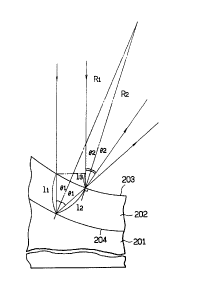
Figure 3 is an enlarged view for a portion of a conven-
tional light receiving member in which a light receiv~ng
layer of a multi-layered structure is deposited on the support,
the surface of which is regularly roughened. In the drawing,- -
301 is a photosensitive layer, 302 is a surface layer, 303
is a free surface and 304 is an interface between the photo-
sensitive layer and the surface layer. As shown in Figure 3,
in the case of merely roughening the surface of the support
regularly by grinding or like other means, since the light
receiving layer is usually formed along the uneven shape at
the surface of the support, the slope of the unevennes~ at the
surface of the support and the slope of the unevenness of~the
light receiving layer are in parallel with each other.
Owing to the parallelism, the following problems always
occur, for example, in a light receiving member of multi-
layered structure in which the light receiving layer comprises
two layers, that is, the photosensitive layer 301 and the
surface layer 302. Since the interface 304 between the photo-
sensitive layer and the surface layer is in parallel with the
free surface 303, the direction of the reflected light Rl at
the interface 304 and that of the reflected light R2 at the
free surface 303 coincide with each other and, accordingly,
~ ~854~S
an interference fringe occurs depending on the thickness of
the surface layer.
Figure 2 is an enlarged view for a portion of the light
receiving member according to this invention as shown in
Figure 1. As shown in Figure 2, an uneven shape composed
of a plurality of fine spherical dimples each of which having
an inside face provided with minute irregularities (not shown)
is formed at the surface of the support in the light receiving
member according to this invention and the light receiving
layer thereover is deposited along the uneven shape. Therefore,
in the light receiving member of the multi-layered structure,
for example, in which the light receiving layer constituted
by a photosensitive layer 201 and a surface layer 202, the
interface 204 between the photosensitive layer 201 and the
surface layer 202 and the free surface 203 are respectively
formed following the uneven shape composed of the spherical
dimples along the uneven shape at the surface of the support.
Assuming the radius of curvature of the spherical dimples
formed at the interface 204 as Rl and the radius of cNrvature
of the spherical dimples formed at the free surface as R2,
since Rl is not identical with R2, the reflection light at the
interface 204 and the reflection light at the free surface 203
have reflection angles different from each other, that is,
~1 is not identical with 2 in Figure 2 and the direction of
their reflection lights are different. In addition, the
- 16 -
~ ~854~5
deviation of the wavelength represented by Ql + Q2 ~ Q3
by using Ql' Q2' and Q3 shown in Figures 2 is not constant
but variable, by which a sharing interference corresponding
to the so-called Newton ring phenomenon occurs and the inter-
ference fringe is dispersed within the dimples. Then, if
the interference ring should appear in the microscopic point
of view in the images caused by way of.the light receiving
member, it is not visually recognized.
That is, in a light receiving member having a light
receiving layer of multi-layered structure formed on the
support having such a surface.shape, the fringe pattern
resulted in the images due to the interference between lights
passing through the light receiving layer and reflecting on
the layer interface and at the surface of the support thereby
enabling to obtain a light receiving member capable of forming
excellent images.
By the way, the radius of curvature R and the width D
of the uneven shape formed by the spherical dimples, at the
surface of the support of the light receiving member according
to this invention constitute an important factor for effectively
attaining the advantageous effect of preventing the occurrence
of the interference fringe in the light receiving member
according to this invention. The present inventors carried
our various experiments and, as a result, found the following
facts.
~ ~85415
That is, if the radius of curvature R and the width D
satisfy the following equation:
D > 0 035
0.5 or more Newton rings due to the sharing interference are
present in each of the dimples. Further, if they satisfy the
following equation:
D ~ 0.055
one or more Newton rings due to the sharing interference are
present in each of the dimples.
From the foregoing, it is preferred that the ratio D/R
is greater than 0.035 and, preferably, greater than 0.055 for
dispersing the interference fringPsresulted throug40ut the
light receiving member in each of the dimples thereby preventing
the occurrence of the interference fringe in the light receiving
member.
Further, it is desired that the width D of the unevenness
formed by the scraped dimple is about 500 ~m at the maximum,
preferably, less than 300 ~m and, re preferably less than
100 ~m.
In addition, it is desired that the height of the minute
irregularity to be provided with the inside face of the spherical
dimple of the support, namely the surface roughness Ymax of
the inside face of the spherical dimple lies in the range of
0.5 to 20 ~m.
::
:
- 18 -
,
~ ~854~5
That i5, in the case where said r is less than 0.5
max
~m, a sufficient scattering effect is not given. And in the
case where it e~ceeds 20 ~m, the magnitude of the minute
irregularity becomes undesirably greater in comparison with
that of the spherical dimple to prevent it from being formed
in a desired spherical form and result in bringing about such
a light receiving member that does not sufficiently prevent
the occurrence of the interference fringe. In addition to
this, when a light receiving layer is deposited on such
support, the resulting light receiving member becomes to have
such a light receiving layer that is accompanied by an
undesirably grown unevenness being apt to invite defects
in visible images to be formed.
The present invention has been completed on the basis
of the above-mentioned findings.
The light receiving layer of the light receiving-member
which is disposed on the support having the particular surface
as above-mentioned in this invention is constituted by the
photosensitive layer and the surface layer. The photosensitive
layer is composed of amorphous material containing silicon
atoms and at least either germanium atoms or tin atoms,
particularly preferably, of amorphous material containing
silicon atoms(Si), at least either germanium atoms(Ge) or
tin atoms(Sn), and at least either hydrogen atoms(H) or
halogen atoms(X) [hereinafter referred to as "a-Si(Ge,Sn)(H,X)"]
-- 19 --
~28541S
or of a-Si(Ge,Sn)(H,X) containing at least one kind selected
from oxygen atoms(O), carbon atoms(C),and nitrogen atoms(N)
[hereinafter referred to as "a-Si(Ge,Sn)(O,C,N)(H,X)"].
And said amorphous materials may contain one or more kinds
of substances control the conductivity in the case where
necessary.
The photosensitive layer may be a multi-layered structure
and, particularly preferably, it includes a so-called barrier
layer composed of a charge injection inhibition layer and/or
electrically insulating material containing a substance for
controlling the conductivity as one of the constituent layers.
As for the surface layer, it is composed of amorphous
material containing silicon atoms, and at least one kind
selected from oxygen atoms, carbon atoms and nitrogen atoms,
and particularly preferably, of amorphous material containing
silicon atoms(Si), at least one kind selected from oxygen atoms
(O), carbon atoms(C) and nitrogen atoms(N), and at least either
hydrogen atoms(H) or halogen atoms(X). [hereinafter referred
to as "a-Si(O,C,N)(H,X)"].
For the preparation of the photosensitive layer and the
surface layer of the light receiving member according to this
invention, because of the necessity of precisely controlling
their thicknesses at an~optical level in order to effectively
achieve the foregoing objects of this invention there is
usually used vacuum deposition technique such as glow discharging
- 20 -
~ ~54~5
method, sputtering method or ion plating method, but optical
CVD method and heat CVD method may be also employed.
The light receiving member according to this invention
will now be explained more specifically referring to the
drawings. The description is not intended to limit the scope
of this invention.
Support 101
The support 101 in the light receiving member according
to this invention has a surface with fine unevenness smaller ,
than the resolution power required for the light receiving
member and the unevenness is composed of a plurality of fine
spherical dimples each of which having an inside face provided
with minute irregularities.
The shape of the surface of the s,upport and an example
of the preferred methods of preparing the shape are specifically
explained referring to Figures 4, 5(A), 5tBI and 5(C) but it
should be noted that the shape of the support in the light
receiving member of this invention and the method of preparing
the same are no way limited only thereto.
Figure 4 is a schematic view for a typical example of the
shape at the surface of the support in the light receiving
member according to this invention, in which a portion of
the uneven shape is enlarged.
In Figure 4, are shown a support 401, a support surface
402, an irregular shape due to a spherical dimple (spherical
- 21 -
~ ~5415
cavity pit) 403, an inside face of the spherical dimple 404
which is provided with minute irregularities and a rigid
sphere 403' having a surface 4041 which is provided with
minute irregularities.
Figure 4 also shows an example of the preferred methods
of preparing the surface shape of the support.
That is, the rigid sphere 403' is caused to fall from
a position at a predetermined height above the support
surface 402 and collides against the support surface 402
thereby forming the spherical dimple 403 having the inside
face provided with minute irregularities 404. And a plurality
of the spherical dimples each substantially of an almost
identical radius of curvature R and of an almost identical
width D can be formed to the support surface 402 by causing
a plurality of the rigid spheres 403' substantially of an
identical diameter of curvature R' to fall from identical
height _.simultaneously or sequentially.
Figures 5(A) through 5(C) show typical embodiments of
supports formed with the uneven shape composed ~f a plurality
of spherical dimples each of which having an inside face.
provided with minute irregularities at the support surface as
described above.
In Figures 5(A) through 5(C), are shown a support 5Ql,
a support surface 5~)2, a spherical dimple (spherical cavity
pit) having an inside face provided with minute irregularities
:- -- 22 --
~ ~35415
(not shown) 504 or 504' and a rigid sphere of.which surface
has minute irregularities (not shown) 503 or 503'.
In the embodiment shown in Figure 5(A), a plurality of
the dimples (spherical cavity pits) 503, 503, ... of an almost
identical radius of curvature and of an almost identical width
are formed while being closely overlapped with each other
thereby forming an uneven shape regularly by.causing to fall
a plurality of spheres 503', 503', ... regularly from an
identical height to different positions at the support surface
502 of the support 501. In this case, it is naturally required
for forming the dimples 503, 503, ... overlapped with each
other that the spheres 503'j 503', ... are gravitationally
dropped such that the times of collision of the respective
spheres 503', 503', ... to the support surface 502.are displaced
from each other.
Further, in the embodiment shown in Figure 5(B), a plurality
of dimples 504, 504', ... having two kinds of diameter of
curvature and two kinds of width are formed being densely
overlapped with each other to the surface 502 of the support
501 thereby forming an unevenness with irregular height at the
surface by dropping two kinds of spheres 503, 503', ... of
different diameters from the heights identical with or different
from each other.
Further re, in the embodiment shown in Figure 5(C)
(front elevational and cross-sectional views for the support
- 23 -
. . .
~ ~85415
surface), a plurality of dimples S04, 504, ... of an almost
identical diameter of curvature and plural kinds of width are
formed while being overlapped with each other thereby forming
an irregular unevenness by causing to fall a plurality of
spheres 503, 503, ... of an identical diameter from the
identical height irregularly to the surface 502 of the support
501.
As described above, the uneven shape of the support
surface composed of the spherical dimples each of which having
an inside face provided with irregularities can be formed
preferably by dropping the rigid spheres respectively of a
surface provided with minute irregularities to the support
surface. In this case, a plurality of spherical dimples having
desired radius of curvature and width can be formed at a
predetermined density on the support surface by properly
selecting various conditions such as the diameter of the rigid
spheres, falling height, hardness for the rigid sphere and the
support surface or the amount of the fallen spheres. That is,
the height and the pitch of the uneven shape formed for the
support surface can optionally be adjusted depending on the
given purpose by selecting various conditions as described
above thereby enabling to obtain a support having a desired
uneven shape with the support surface.
For making the surface of the support into an uneven shape
in the light receiving member, a method of forming such a shape
- 24 -
~.~85415
by the grinding work by means of a diamond cutting tool using
lathe, milling cutter, etc. has been proposed, which will be
effective to some extent. However, the method leads to problems
in that it requires to use cutting oils, remove cutting dusts
inevitably resulted during cutting work and to remove the
cutting oil remaining on the cut surface,~ which after all
compli~ates the fabrication and reduces the working efficiency.
In this invention, since the uneven surface shape of the
support is formed by the spherical dimples as described above,
a support having the surface with a desired uneven shape can
conveniently be prepared with no problems as described above
at all.
The support 101 for use in this invention may either be
electroconductive or insulative. The electroconductive
support can include, for example, metals such as NiCr, stainless
steel, Al, Cr, Mo, Au, Nb, Ta, V, Ti, Pt, and Pb, or the alloys
thereof.
The electrically insulative support can include, for
example, film or sheet of synthetic resins such as polyester,
polyethylene, polycarbonate, cellulose acetate, polypropylene,
polyvinyl chloride, polyvinylidene chloride, polystyrene, and
polyamide; glass, ceramics, and paper. It is preferred that
the electrically insulative support is applied with electro-
conductive treatment to at least one of the surfaces thereof
and disposed with a light receiving layer on the thus treated
- 25 -
~ ?.8S415
surface.
In the case of glass, for instance, electroconductivity
is applied by disposing, at the surface thereof, a thin film
made of NiCr, Al, Cr, Mo, Au, Ir, Nb, Ta, V, Ti, Pt, Pd, In202,
SnO3, ITO (In203 + SnO2), etc. In the case of the synthetic
resin film such as polycarbonate film, the electroconductivity
is provided to the surface by disposing a thin film of metal
such as NiCr, Al, Ag, Pb, Zn, Ni, Au, Cr, Mo, Ir, Nb, Ta, V,
Tl, and Pt by means of vacuum deposition, electron beam vapor
deposition, sputtering, etc. or applying lamination with the
metal to the surface. The support may be of any configuration
such as cylindrical, belt-like or plate-like shape, which can
be properly determined depending on the applications. For
instance, in the case of using the light receiving member shown
in Figure 1 as image forming member for use in electronic
photography, it is desirably configurated into an endless belt
or cylindrical form in the case of continuous high speed produc-
tion. The thickness of the support member is properly determined
so that the light receiving member as desired can be formed.
In the case where flexibility is required for the light
receiving member, it can be made as thin as possible within
a range capable of sufficiently providing the function as the
support. However, the thickness is usually greater than 10 ~m
in view of the fabrication and handling or mechanical strength
of the support.
~.~85415
Explanation will then be made to one embodiment of a
device for preparing the support surface in the case of using
the light receiving member according to this invention as the
light receiving member for use in electronic photography while
referring to Figures 6 (A) and 6(B), but this invention is no
way limited only thereto.
In the case of the support for the light receiving member
for use in electronic photography, a cylindrical substrate is
prepared as a drawn tube obtained by applying usual extruding
work to aluminum alloy or the like other material into a boat
hall tube or a mandrel tube and further applying drawing work,
followed by optical heat treatment of tempering. Then, an
uneven shape is formed at the surface of the support at the
cylindrical substrate by using the fabrication device as
shown in Figures 6(A) and 6(B).
The rigid sphere to be used for forming the uneven shape
as described above on the support surface can include, for
example, various kinds of rigid spheres made of stainless steel,
aluminum, steel, nickel, and brass, and like other metals,
ceramics, and plastics. Among all, rigid spheres of stainless
steel or steel are preferred in view of the durability and the
reduced cost. The hardness of such sphere may be higher or
lower than that of the support. However, in the case of using
the rigid spheres repeatedly, it is desired that the hardness
of sphere is higher than that of the support.
~ ~854i5
In order to form the particular shape as above mentioned
for the support surface, it is necessary to use a rigid sphere
of a surface provided with minute irregularities.
Such rigid sphere may be prepared properly in accordance
with a mechanical treatment method such as a method utilizing
plastic processing treatment such as embossing and wave adding
- and a surface roughening method su¢h as-sating finishing, or
a chemical treatment method such as acid etching or alkali
etching.
And the shape (height) or the hardness of the irregularities
as formed on the surface of the rigid sphere may be adjusted
properly by subjecting the rigid sphere to the surface treatment
in acco~dance with electropolishing, chemical polishing or
- finish polishing, or anodic oxidation coatingj chemical
coating, planting, vitreous enameling, painting, evaporation
film forming or CVD film forming.
Figures 6(A) and 6tB) are schematic cross-sectional views
for the entire fabrication device, in which are sh~own an aluminum
cylinder 601 for preparing a support, and the cylinder 601 may
preveously be finished at the surface to an appropriate smooth-
ness. The cylinder 601 is supported by a rotating shaft 602,
driven by an appropriate drive means 603 such as a motor and
made rotatable around the axial center. The rotating speed is
properly determined and controlled while considering the density
of the spherical dimples to be formed and the amount of rigid
- 28 -
~ ~854~S
spheres supplied.
A rotating vessel 604 is supported by the rotating shaft
602 and rotates in the same direction as the cylinder 601 does.
The rotationg vessel 604 ~ontains a plurality of rigid spheres
each of which having a surface provided with minute irregular-
ities 605,.605, ... The rigid spheres are held by plural
projected ribs 606, 606, ... being disposed on the inner wall
of the rotating vessel 604 and transported to the upper position
by the rotating action of the rotating vessel 604. .The rigid .
spheres 605, 605, ... then continuously fall down and collide
against the surface of the cylinder 601 thereby forming a
plurality of spherical dimples each of which having an inside
face provided with irregularities when the revolution speed
of the rotating vessel 605 is maintained at an appropriate rate.
The fabrication device can be structured in the following
way. That is, the circumferential wall of the rotating vessel
604 are uniformly perforated so as to allow the passage of a
washing liquid to be jetting-like supplied from one or more of
a showering pipe 607 being placed outside the rotating vessel
604 thereby having the cylinder 601, the rigid spheres 605,
605, ... and also the inside of the rotating vessel 604 washed
with the washing liquid.
In that case, extraneous matter caused due to static
electricity generated by contacts between the rigid spheres or
between the rigid spheres and the inside part of the rotating
- 29 -
~' ~ . . .
.
~ ~854~5
vessel can be washed away to form a desirable shape to the
surface of the cylinder being free from such extraneous
matter. As the washing liquid, it is necessary to use such
that does not give any dry unevenness or any residue. In this
respect, a fixed oil itself or a mixture of it with a washing
liquid such as trichloroethane or trichloroethylene are
preferable.
Photosensitive Layer
In the light receiving member of this invention, the
photosensitive layer 102 is disposed on the above-mentioned
support. The photosensitive layer is composed of a-Si(Ge,Sn)
(H,X) or a-Si(Ge,Sn)(O,C,N~(H,X), and preferably it contains
a substance to control the conductivity.
The halogen atom(X) contained in the photosensitive layer
include, specifically, fluorine, chlorine, bromine and iodine,
fluorine and chlorine being particularly preferred. The
amount of the hydrogen atoms(H), the amount of the halogen
atoms(X2 or the sum of the amounts for the hydrogen atoms
and the halogen atoms (H+X~ contained in the photosensitive
layer 102 is usually from 1 to 40 atomic% and, preferably,
from 5 to 30 atomic%.
In the light receiving member according to this invention,
the thickness of the photosensitive layer is one of the important
factors for effectively attaining the purpose of this invention
and a sufficient care should be taken therefor upon designing
- 30 -
~ ~354~5
-the light receiving member so as to provide the member with
desired performance~ The layer thickness is usually from 1
to 100 ~m, preferably from 1 to 80 ~m and, more preferably,
from 2 to 50 ~m.
Now, the purpose of incorporating germanium atoms and/or
tin atoms in the photosensitive layer of the light receiving
member according to this invention is chiefly for the improve-
ment of an absorption spectrum property in the long wavelength
region of the light receiving member.
That is, the light receiving member according to this
invention becomes to give excellent-various properties by
incorporating germanium atoms and/or tin atoms into the photo-
sensitive layer. Particularly, it becomes more sensitive to
light of wavelengths broadly ranging from short wavelength to
long wavelength covering visible light and it also becomes
quickly responsive to light.
This effect becomes more significant when a semiconductor
laser emitting ray is used as the light source.
In the photosensitive layer of the light receiving member
according to this invention, it may contain germanium atoms
and/or tin atoms either in the entire layer region or in the
partial layer region adjacent to the support.
In the latter case, the photosensitive layer becomes to
have a layer constitution that a constituent layer containing
germanium atoms and/or tin atoms and another constituent layer
~ ~354~5
containing neither germanium atoms nor tin atoms are laminated
in this order from the side of the support.
And either in the case where germanium atoms and/or tin
atoms are incorporated in the entire layer region or in the
case where incorporated only in the partiaL layer region,
germanium atoms.and/or tin atoms may be distributed therein
either uniformly or unevenly. (The uniform distribution means
that the distribution of germanium atoms and/or tin atoms in
the photose~sitive layer is.uniform both in the.direction
parallel with the surface of the support and in the thickness
direction. The uneven distribution means that the distribution
of germanium atoms and/or tin atoms in the photosensitive layer
is uniform in the direction parallel with the surface of the
support but is uneven in the thickness direction.)
And in the photosensitive layer of the light receiving
member according to this invention, it is desirable that
germanium atoms and/or tin atoms in the photosensitive layer
be present in the.side region adjacent to the support in a
relatively large a unt in uniform distribution state or be
present more in the support side region than in the free
surface side region. In these cases, when the distributing
concentration of germanium atoms and/or tin atoms are extremely
heightened in the side region adjacent to the support, the
light of long wavelength, which can be hardly absorbed in the
constituent layer or the layer region near the free surface
- 32 -
~ ?J~35415
side of the light receiving layer when a light of long wave-
length such as a semiconductor emitting ray is used as the
light source, can be substantially and completely absorbed in
the constituent layer or in the layer region respectively
adjacent to the support for the light receiving layer. And
this is directed to prevent-the interference caused by the
light reflected from the surface of-the support.
As above explained, in the photosensitive layer of the
ligh~ receiving member acco~ding~to this invention, germanium
atoms and/or tin atoms may be distributed either uniformly
in the entire layer region or the partial constituent layer
region or unevenly and continuously in the direction of the
layer thickness in the entire layer region or the partial
constituent layer region.
In the following an explanation is made of the typical
examples of the distribution of germanium atoms in the
thckness direction in the photosensitive layer, with reference
to Figures 7 through 15.
In Figures 7 through 15, the abscissa represents the
distribution concentration C of germanium atoms and the
ordinate represents the thickness of the entire photosensitive
layer or the partial constituent layer adjacent to the support;
and tB represents the extreme position of the photosensitive
layer adjacent to the support, and tT represent the other
extreme position adjacent to the surface layer which is away
~ ~85415
from the support, or the position of the interface between
the constituent layer contalning germanium atoms and the
constituent layer not containing germanium atoms.
That is, the photosensitive layer containing germanium
atoms is formed from the tB side toward tT side.
In these figures, the thickne-ss and concentration are
schematically exaggerated to help understanding.
Figure 7 shows the first typical example of the thickness-
wise distribution of germanium atoms in the photosensitive
layer.
In the example shown in Figure 7, germanium atoms are
distributed such that the concentration C is constant at a
value Cl in the range from position tB (at which the photo-
sensitive layer containing germanium atoms is in contact with
the surface of the support) to position tl, and the concentra-
tion C gradually and continùously decreases from C2 in the
range from position tl to position tT at the interface.
The concentration of germanium atoms is substantially zero
at the interface position tT. ("Substantially zero" means
that the concentration is lower than the detectable limit.)
In the example shown in Figure 8, the distribution of
germanium atoms contained in such that concentration C3 at
position tB gradually and continuously decreases to concentra-
tion C4 at position tT.
In the example shown in Figure 9, the distribution of
-34 -
~.~85415
germanium atoms is such that.concentration C5 is constant
in the range from position tB and position t2 and it gradually
and continuously decreases in the range from position t2 and
position tT. The concentration at position tT is substantially
zero.
In the example shown in Figure 10, the distribution of
germanium atoms is such that concentration C6 gradually and
continuously decreases in the range from position tB and
position t3, and it sharply and continuously decreases in the
range rom position t3 to position tT. The concentration at
position tT is substantially zero.
In the example shown in Figure 11, the distribution of
germanium atoms C is such that concentration C7 is constant
in the.range from position tB and position t4 and it linearly
decreases in the range from position t4 to position tT. The
concentration at position tT is zero.
In the example shown in Figure 12, the distribution of
germanium atoms is such that concentration C8 is constant in
the range from position tB and position t5 and concentration
Cg linearly decreases to concentration C10 in range from
position t5 to position tT.
In the example shown in Figure 13, the distribution of
germanium atoms is such that concentration linearly decreases
to zero in the range from position tB to position tT.
In the example shown in Figure 14, the distribution of
~ ~35415
germanium atoms is such that concentration C12 linearly
decreases to C13 in the range from position tB to pasition t6
and concentration C13 remains constant in the range from
position t6 to position tT.
In the example shown in Figure 15, the distribution of
germanium atoms is such that concentration C14 at position tB
slowly decreases and then sharply decreases to concentration
C15 in the range from position tB to position t7.
In the range from position t7 to.position t8, the concen- . .
tration sharply decreases at first and slowly decreases to C16.
at position t8. The concentration slowly decreases to C17
between position t8 and position tg~ Concentration C17 further
decreases to substantially zero between position tg and
position tT~ The concentration decreases as shown by the.
curve.
Se~eral examples of the thicknesswise distribution of
germanium atoms and/or tin atoms in the layer 102' have been
illustrated in.Figures 7 through 15. In the light receiving
member of this invention, .the concentration of germanium atoms
and/or tin atoms in the photosensitive layer should preferably ..
be high at the position adjacent to the support and considerably
low at the position adjacent to the interface tT.
In other words, it is desirable that the photosensitive
layer constituting the light receiving member of this invention
have a region adjacent to the support in which germanium atoms
- 36 -
~ ~85415
and/or tin atoms are locally contained at a comparatively
high concentration.
Such a local region in the light receiving member of
this invention should preferably be formed within 5 ~m from
the interface tB.
The local region may occupy entirely or partly the
thtckness of 5 ~m from the lnterface position tB.
Whether the local region should occupy entirely or partly
the layer depends on the performance required for the light
receiving layer to be formed.
The thicknesswise distribution of germanium atoms and/or
tin atoms contained in the local region should be such that
the m~ximum concentration Cmax of germanium atoms and/or tin
atoms is greater than 100~ atomic ppm, preferably greater than
5000 atomic ppm, and re preferably greather than 1 x 10⁴
atomic ppm based on the amount of silicon atoms.
In other words, ~n the light receiving member of this
invention, the photosensitive layer which contains germanium
atoms and~or tin atoms should preferably be formed such that
the maximum concentration Cmax of their distribution exists
within 5 ~m of the thickness from tB (or rom the support side).
In the light receiving member of this invention, the
amount of germanium atoms and/or tin atoms in the photosensitive
layer should be properly determined so that the object of the
invention is effectively achieved. It is usually 1 to 6 x 10⁵
- 37 -
8S415
atomic ppm, preferably 10 to 3 x 10⁵ atomic ppm, and more
preferably 1 x Io2 to 2 x 10⁵ atomic ppm.
The photosensitive layer of the light receiving member
of this invention may be incorporated with at least one kind
selected from oxygen atoms, carbon atoms, nitrogen atoms.
This is effective in increasing the photosensitivity and
dark resistance of the light receiving ~ember and also in
improving adhesion between the support and the light receiving
layer.
In the case of incorporating at least one kind selected
from oxygen atoms, carbon atoms, and nitrogen atoms into the
photosensitive layer of the light receiving member according
to this invention, it is performed at a uniform.distribution
or.uneven distribution in the direction o~ the layer thickness
depending on the purpose or the expected effects as described
above, and accordingIy, the co.ntent is varied dependihg on
them.
That is, in the case of increasing the photosensitivity,
the dark resistance of the light receiving member, they are-
contained at a uniform distribution over the entire layer
region of the photosensitive layer. In this case, the amount
of at least one kind selected from carbon atoms, oxygen atoms,
and nitrogen atoms contained in the photosensitive layer may
be relatively small.
In the case of improving the adhesion between the support
,~ .
- 38 -
~ ~854~S
and the photosensitive layer, at least one kind selected from
carbon atoms, oxygen atoms, and nitrogen atoms is contained
uniformly in the layer constituting the photosensitive layer
adjacnet to the support, or at least one kind selected from
carbon atoms, oxygen atoms, and nitrogen atoms is contained
such that the distribution concentration is higher at the end
of the photosensitive layer on the side of the support. In
this case, the amount of at least one kind selected from
oxygen atoms, carbon atoms, and nitrogen atoms is comparatively
large in order to improve the adhesion to the support.
The amount of at least one kind selected from oxygen atoms,
carbon atoms, and nitrogen atoms contained in the photosensitive -
layer of the light receiving member according to this invention
is also determined while considering the organic relationship
such as the performance at the interface in contact with the
support, in addition to the performance-required for the light
receiving layer as described above and it is usually from 0.001
to 50 atomic%, preferably, from 0.002 to 40 atomic%j and,
most suitably, from 0.003 to 30 atomic%.
By the way, in the case of incorporating the element in
the entire layer region of the photosensitive layer or the
proportion of the layer thickness of the layer region incorpo-
rated with the element is greater in the layer thickness of the
light receiving layer, the upper limit for the content is made
smaller. That is, if the thickness of the layer region
- 39 -
~as4~s
incorporated with the element is 2/5 of the thickness for
the photosensitive layer, the content is usually less than
30 atomic%, preferably, less than 20 atomic% and, more
suitably, less than 10 atomic%.
some typical examples in which a relatively large
amount of at least one kind selected from oxygen atoms,
carbon atoms, nitrogen atoms is contained in the
photosensitive layer according to this invention on the
side of the support, then the amount is gradually decreased
from the end on the side of the support to the end on the
side of the free surface and decreased further to a
relatively small amount or substantially zero near the end
of the photosensitive layer on the side of the free surface
will be hereunder explained with reference to Figures 16
through 24. However, the scope of this invention is not
limited to them.
The content of at least one of the elements selected
from oxygen atoms (O), carbon atoms(C) and nitrogen atoms
(N) is hereinafter referred to as "atoms(O,C,N)".
In Figures 16 through 24, the abscissa represents the
distribution concentration C of the atoms (O.C.N) and the
ordinate represents the thickness of the photosensitive
layer; and t~ represents the interface position between the
support and the photosensitive layer and tT represents the
interface position between the free surface and the
photosensitive layer.
Figure 16 shows the first typical example of the
thickness-
- 40 -
.
1 ~5~5
wise distribution of the atoms(O,C,N) in the photosensitive
layer. In this example, the atoms(O,C,N) are distributed in
the way that the concentration C remains constant at a value
Cl in the range from.position tB (at which the photosensitive
layer comes into contact with the support) to position t1,
and the concentration C gradually and continuously decreases
from C2 in the range from position tl to position tT,.where
the concentration of the group III atoms or group ~ atoms is
c3.
In the example shown in Figure 17, the distribution
concentration C of the atoms(O,C,N) contained in the photo-
sensiti~e layer is such that concentration C4.at position tB
continuously decreases to concentration C5 at position t
In the example shown in Figure 18, the distribution..
concentration C of the atoms(O,C,N) is such that concentration
C6 remains constant in the range from position tB and position
t2 and it gradually and continuously decreases in the range
from position t2 and position tT. The concentration at
position tT is substantially zero.
In the example shown in Figure.l9, the distribution
concentration C of the atoms(O,C,N) is such that concentration
C8 gradually and continuously decreases in the range from
position tB and position tT, at which it is substantially zero.
In the example shown in Figure 20, the distribution
concentration C of the atoms(O,C,N) is such that.concentration
- 41 -
~ ~.854~5
Cg remains constant in the range from position tB to position .
t3, and concentration C8 linearly decreases to concentration
C10 in the range from position t3 to position tT.
In the example shown in Figure 21, the distribution
concentration C of the atoms(O,C,N) is such that concentration
Cll remains constant in the range from position tB and
position t4 and it linearly decreases to C14 in the range from
position t4 to position tT~
In the example shown in Figure 22, the distribution con-
centration C of the atoms(O,C,N) is such that concentration
C14 linearly decreases in the range from position tB to position
tT~ at which the concentration is substantially zero.
~ In the example shown in Figure 23, the distribution con-
centration C of the atoms(O,C,N) is such that concentration
C15 linearly decreases to concentration ~16 in the range from
position tB to position t5 and concentration C16 remains
constant in the range from position t5 to position tT.
Finally, in the example shown in Figure 24, .the distribution
concentration C of the atoms(O,C,N) is such that concentration
C17 at position tB slowly decreases and then sharply decreases .
to concentration C18 in the range from position tB to position
t6. In the range from position t6 to position t7, the concen-
trantion sharply decreases at first and slowly decreases to Clg
at position t7. The concentration slowly decreases between
position t7 and position t8, at which the concentration-is C20.
- 42 -
~ ?~5415
Concentration C20 slowly decreases to substantially zero
between position t8 and position tT~
As shown in the embodiments of Figures 16 through 24,
in the case where the distribution concentration C of the
atoms(O,C,N) is higher at the portion of the photosensitive
layer near the side of the support, while the distribution
concentration C is considerably lower or substantial-ly reduced
to zero in the portion of the photosensitive layer is the
vicinity of the free surface, the improvement in the adhesion
of the photosensitive layer with the support can be more
effectively attained by disposing a localized region where
the distribution concentration of the atoms(O,C,N) is relatively
higher at the portion near the side of the support, preferably,
by disposing the localized region at a position within S ~m
from the interface position adjacent to the support surface.
The localized region may be disposed partially or entirely
at the end of the light receiving layer to be contained with
the atoms(O,C,N) on the side of the support, which may be
properly determined in accordance with the performance required
for the light receiving layer to be formed.
It is desired that the amount of the atoms(O,C,N) contained
in the localized region is such that the maximum value of the
distribution concentration C of the atoms(O,C,N) is greater
than 500 atomic ppm, preferably, greater than 800 atomic ppm,
most suitably greater than 1000 atomic ppm in the distribution.
- 43 -
~ ~8~;4~5
In the photosensitive layer of the light receiving
member according to this invention, a substance for control-
ling the electroconductivity may be contained to the light
receiving layer in a uniformly or unevenly distributed state
to the entire or partial layer region.
As the substance for controlling the conductivity,
so-called impurities in the field of the semiconductor can be
mentioned and those usable herein-can include atoms belonging
to the group III of the periodic table that provide p-type
conductivity (hereinafter simply referred to as "group III
atoms") or atoms belonging to the group V of the periodic table
that provide n-type conductivity (hereinafter simply referred
to as "group V atoms"). Specifically, the group III atoms can -
include B (boron), Al (aluminum), Ga ~gallium), In (indium),
and Tl (thallium), B and Ga being particularly preferred. The
group V atoms can include, for example,P (phosphorus), As
(arsenic), Sb (antimony), and Bi (bismuth), P and Sb being
particularly preferred.
In the case of incorporating the group III or group V atoms
as the substance for controlling the conductivity into the
photosensitive layer of the light receiving member according
to this invention, they are contained in the entire layer region
or partial layer region depending on the purpose or the expected
effects as described below and the content is also varied.
That is, if the main purpose resides in the control for
- 44 -
~ ~35415
the conduction type and/or conductivity of the photosensitive
layer, the substance is contained in the entire layer region
of the photosensitive layer, in which the content of group III
or group V atoms may be relatively small and it is usually
from 1 x 10 3 to 1 x 10³ atomic ppm, preferably from 5 x 10 2
to 5 x 10² atomic ppm, and most suitably, from 1 x 10 1 to
5 x 10² atomic ppm.
In the case of incorporating the group III or group V
atoms in a uniformly distributed state to a portion of the
layer region in contact with the support, or the atoms are
contained such that the distribution density of the group III
or group V atoms in the direction of the layer thickness is
higher on the side adjacent to the support, the constituting
layer containing such group III or group V atoms or the layer
region containing the group III or group V atoms at high
concentration functions as a charge injection inhibition layer.
That is, in the case of incorporating the group III atoms,
movement of electrons injected from the side of the support
into the photosensitive layer can effectively be-inhibited
upon appIying the charging treatment of at positive polarity
at the free surface of the photosensitive layer. While on
the other hand, in the case of incorporating the group III
atoms, movement of positive holes injected from the side of
the support into the photosensitive layer can effectively be
inhibited upon applying the charging treatment at negative
- 45 -
~ ?~54~S
polarity at the free surface of the layer. The content in
this case is relatively great. Specifically, it is generally .
from 30 to 5 x 10⁴ atomic ppm, preferably from 50 to 1 x 10⁴
atomic ppm, and most suitably from 1 x 10² to 5 x 10³ atomic
ppm. Then, for the charge injection ihibition layer to
produce the intended effect, the thi.ckness (T) of the photo-
sensitive layer and.the thickness (t) of the.layer or layer
region containing the group III.or group v atoms adjacent to
the support should be determined such that the relation.
t/T < 0.4 is established. More preferably, the value for
the relationship.is less than 0.35 and, mo$t suitably, less
than 0.3. Further, the thickness (t) of the layer or layer
region is generally 3 x 10 3 to 10 ~m, preferably 4 x 10 3
to 8 ~m, and, most suitably, 5 x 10 3 to 5 ~m.
Further, typical embodiments in which the group III or
group V atoms incorporated into the light receiving layer is
so distributed that the amount therefor is relatively great
on the side of the support, decreased from the support toward .
the free surface of the light receiving layer, and is relatively
smaller or substantially equal to zero near the end on the
side of the free surface, may be explained on the analogy of
the examples in which the photosensitive layer contains the
~ atoms(O,C,N) as shown-in Figures 16 to 24. However, this
: invention is no way limited only to these embodiments.
As shown in the embodiments of Figures 16 through 24,
- 46 -
35415
in the case where the distribution density C of the group
III or group V atoms is higher at the portion of the light
receiving layer near the side of the support, while the
distribution density C is considerably lower.or substantially
reduced to zero in the interface between the photosensitive
layer and the surface layer, the foregoing effect that the
layer region where the group III or group V atoms are
distributed at a-higher density can form the charge injection
inhibition layer as described above more effectively, by
disposing-a locallized region.where the distribution density
of the group III or group V atoms is relatively higher at the
portion near the side of the support, preferably, by disposing
the localized region at a position within S ~ from the interface
position in adjacent with the support surface.
While the individual effects have been described above
for the distribution state of the gr.oup III or group V atoms,
the distribution state of the group III or group V atoms and
the amount of the group III or group V atoms are, of course,
combined properly as required for obtaining the light receiving .
member having performances capable of attaining a desired
purpose. For instance, in.the case of disposing the charge
injection inhibition layer at the end of the photosensitive
layer on the side of the support, a substance for controlling
the conductivity of a polarity different from that of the
substance for controliing the conductivity contained in the
- 47 -
S~15
charge injection inhibition layer may be contained in the
photosensitive layer other than the charge injection
inhibition layer, or a substance for controlling the
conductivity of the same polarity may be contained by an
amount substantially smaller than that contained in the
charge inhibition layer.
Further, in the light receiving member according to
this invention, a so-called barrier layer composed of
electrically insulating material may be disposed instead
of the charge injection inhibition layer as the constituent
layer disposed at the end on the side of the support, or
both of the barrier layer and the charge injection
inhibition layer may be disposed as the constituent layer.
The material for constituting the barrier layer can
include, for example, those inorganic electrically
insulating material such as Al203, SiO2 and Si3N4 or organic
electrically insulating material such as polycarbonate.
Surface Layer
The surface layer 103 of the light receiving member
according to this invention is disposed on the foregoing
photosensitive layer 102 and has the free surface 104.
The surface layer 103 comprises a-Si containing at
least one of the elements selected from oxygen atoms(0),
carbon atoms(C) and nitrogen atoms (N) and, preferably, at
least one of the elements of hydrogen atoms(H) and halogen
atoms(X)
- 48 -
~.
~ ~854~5
(hereinafter referred to as "a-Si(O,C,N~(H,X)"), and it
provides a funct~on of reducing the reflection of the
incident light at the free surface 104 of the light receiving
member and increasing the transmission rate, as well as a
function of improving various properties such as moisture
proofness, property for continuous repeating use, electrical
voltage withstanding property,.circumstan.tial-resistant
property and durability of the light receiving member.
In this case, it is necessary to constitute such that
the optical band gap Eopt possessed by the surface layer
and the optical ba~d gap Eopt possessed by the photosensitive
layer 102 directly disposed with the surface layer 103 are
matched at the interface between the surface layer 103 and
the photosensitive layer 102, or such optical band gaps are
matched to such an extent as capable of substantially prevent-
ing the reflection of the incident light at the interface
between the surface layer 103 and the photosensitive layer 102.
Further, in addition to the conditions as described -
above, it is desirable to constitute such that the optical
band gap Eopt possessed by the surface layer is sufficiently
larger at the end of the surface layer 103 on the side of
the free surface for ensuring a sufficient amount of the
incident light reaching the photosensitive layer 102 disposed
below the surface layer. Then, in the case of adapting the
optical ba~d gaps at the interface between the surface layer
- 49 -
~ ~54~;
103 and the photosensitive layer 102, as well as ma~ing
the optical band gap Eopt sufficiently larger at the end
of the surface layer on the side of the free surface, the
optical band gap possessed by the surface layer is continu-
ously varied in the direction of the thickness of the
surface layer.
The value of the optical band gap Eopt of the surface
layer in the direction of the layer thickness.is controlled
by controlling, the content of at least one of the elements
selected from the oxygen atoms(O), carbon atoms(C) and
nitrogen atoms(N~ as the atoms. for adjusting the optical
band gaps contained in the surface layer is control.led.
Specifically, the content of at least one of.the. elements
selected from oxygen atoms(O), carbon atoms(C). and nitrogen
atoms(N) (hereinafter refer~d to as "atoms(O,C,N)") is
adjusted nearly or equal to zero at the end of the photo-
sensitive layer in adjacent with the surface layer.
Then, the amount of the atoms(O,C,N) is continuously
increased from the end of the surface layer on the side of
the photosensitive Iayer to the end on.the side of the free
surface and a sufficient amount of atoms(O,C,N) to prevent
the refléction of the incident light at the free surface is
contained near the end on the side of the free surface.
Hereinafter, several typical examples for the distributed
state of the atoms(O,C,N) in the surface layer are explained
- 50 -
~ ~35415
referring to Figures 2s through 27, but this invention is
no way limited only to these embodiments..
In Figures 25 through 27, the abscissa represents the
distribution density C of the atoms(O,C,N) and silicon atoms
and the ordinate represents the thickness t of the surface
layer, in which tT is the position for the interface between
the photosensitive layer and the surface layer, tF is a
position for the free surface,.the solid line represents.the
variation in the distribution density o the atoms(OjC,N)
and the broken line shows the variation in the distribution
density of the silicon atoms(Si).
Figure 25 shows a first typical em~odiment.for the .-
distribution state of the atoms(O,C,N) and the silicon atoms
(Si~ contained in the.surface layer in the direction of.the
layer thickness. In this embo.diment, the distribution .
density C of the atoms(O,C,N) is increased till the density
is increased from zero to a density Cl from the interface
positio~ tT to the position tl linearly. While on the other
hand, the distribution density.of the silicon atoms is decreased
linearly from a density C2 to a density C3 from the position t
to the position tF. The distribution density C for the atoms
(O,C,N) and the silicon atoms are kept at constant.density C
and density C3 respectively.
In the embodiment shown in Figure 26, the distribution
density C of the atoms(O,C,N) is increased linearly from the
-- 51 --
~.2854~5
~lensity zero to a density,C4 from the interface position tT
to the position t3, while it is kept at a constant density
C4 from the position t3 to the position tF. While on the
other hand, the distribution density C of the silicon atoms
is decreased linearly from a density C5 to a density C6 from
the position tT * the position t2, decreased linearly from
the density C6 to a density C7 from the position t2 to the
position t3, and kept at the constant density C7 from the
position t3 to the position tF~ In the case where the density
of the silicon atoms is high at the initial stage of forming
the surface layer, the film forming rate is increased. In
this case, the film forming rate can be com,pensated by
decreasing the distribution density of the silicon atoms in
the two steps as in this embodiment.
In the embodiment shown in Figure 27, the distribution
density of the atoms(O,C,N) is contin,,uously increased from
zero to a density C8 from the position tT to the position t4,
while the distribution density C of the silicon atoms(Si) is
continuously decreased rom a density Cg to a density,ClO.
The distribution density of the atoms(O,C,N) and the distribu-
tion density of the silicon atoms(Si1 are kept at a constant
density C8 and a constant density ClO respectively rom the
position t4 to the position tF. In the case of continuously
increasing the distribution density of the atoms(O,C,N)
gFadually as in this embodiment, the variation coefficient of
- 52 -
~ 2854~5
the reflective rate in the direction of the layer thickness
of the surface layer can be made substantially constant.
As shown in Figures 25 through 27, in the surface
layer of the light receiving member according to this
invention, it is desired to dispose a layer region in
which the distribution density of the atoms(O,C,N) is made
substantially zero at the end of the surface layer on the
side of the photosensitive layer, increased continuously
toward the free surface and made relatively high at the end
of the surface layer on the side of the free surface. Then,
the thickness of the layer region in this case is usually
made greater than 0.1 ~m for providing a function as the
reflection preventive layer and a function as the protecting
layer.
It is desired that at least one of the hydrogen atoms
and the halogen atoms are contained also in the surface layer,
in which the amount of the hydrogen atoms(H), the amount of
the halogen atoms(X) or the sum of the hydrogen atoms and the
halogen atoms (H~X) are usually from 1 to 40 atm %, preferably,
from S to 30 atm % and, most suitably, from 5 to 25 atm %.
Further, in this invention, the thickness fo the surface
layer is also one of the most important factors for effectively
attaining the purpose of the invention, which is properly
determined depending on the desired purposes. It is required
that the layer thickness is determined in view of the relative
- 53 -
~ ~5415
and organic relationship in accordance with the amount of
the oxygen atoms, carbon atoms, nitrogen atoms, halogen atoms
and hydrogen atoms contained in the surface layer or the
properties required for the surface layer. Further, it
should be determined also from the economical point of view
such as productivity and mass productivity. In view of the
above, the thickness of the surface layer is usually from
3 x 10 3 to 30 ~, preferably, from 4 x 10 3 to 20 ~ and,
particularly preferably, from 5 x 10 3 to 10 ~.
By adopting the layer structure of the light receiving
member according to this invention as described above, all
of the various problems in the light receiving members
comprising the light receiving layer constituted with amorphous
silicon as described above can be overcome. Particularly,
in the case of using the coherent laser beams as a light-
source, it is possible to remarkably prevent the occurrence
of the interference fringe pattern upon forming images due
to the interference phenomenon thereby enabling to obtain
reproduced image at high quality.
Further, since the light receiving member according to
this invention has a high photosensitivity in the entire
visible ray region and, further, since it is excellent in
the photosensitive property on the side of the longer wave-
length, it is suitable for the matching property, particularly,
with a semiconductor laser, exhibits a rapid optical response
- 54 -
~ 2~35415
and shows more excellent electrical, optical and electro-
conductive nature, electrical voltage withstand property
and resistance to working circumstances.
Particularly, in the case of applying the light receiving
member to the electrophotography, it gives no undesired effects
at all of the residual potential to the image formation,
stable electrical propèrties high sensitivity and high S/N
ratio, excellent light fastness and property for repeating
use, high image density and clear half tone and can provide
high quality image with high resolution power repeatingly.
The method of forming the light receiving layer according
to this invention will now be explained.
The amorphous material constituting the light receiving
layer in this invention is prepared by vacuum deposition
technique utilizing the discharging phenomena such as glow
discharging, sputtering, and'ion plating pxacess. These
production processes are properly used selectively depending
on the factors such as the manufacturing conditions, the
installation cost required, production scale and properties
required for the li'ght receiving members to be prepared.
The glow discharging process or sputtering process is suitable
since the control for the condition upon preparing the light
receiving members having desired properties are relatively
easy and carbon atoms and hydrogen atoms can be introduced
easily together with silicon atoms. The glow discharging
~1 ?~85415
process and the sputtering process may be used together in
one identical system.
sasically~ when a layer constituted with a-Si(H,X) is
formed, for example, by the glow discharging process, gaseous
starting material for supplying Si capable of supplying
silicon atoms(Si) are introduced together.with gaseous
startingmaterial for introducing hydrogen atoms(H) and/or
halogen atoms(X) into a deposition chamber the insidepressure
of which can be reduced, glow discharge is generated in the
deposition chamber, and a.layer.composed of a-Si(H,X~ is
formed on the s.urface of a predetermined support disposed
previously at a predetermined position in the chamber !
The gaseous starting material for supplying Si can.include
gaseous or gasifiable silicon hydrides (silanes~ such as SiH4,
2 6 3 8' 4 10' etc., SiH4 and Si2H6 being particularly
preferred in view of the easy layer forming work and the good
efficiency for the supply of Si.
Further, various halogen compounds can be mentioned as
the gaseous starting material for introducing the halogen
atoms and gaseous or gasifiable halogen compounds, for.
example, gaseous halogen, halides, inter-halogen compounds
and halogen-substituted sil.ane derivatives are preferred...
Specifically, they can include halogen gas such as of
fluorine, chlorine, bromine, and iodine; inter-halogen .
compounds such as BrF, ClF, ClF3, BrF2, BrF3, IF7, ICl, IBr,
- 56 -
~ ~85415
etc.; and silicon halides such as SiF4, Si2H6, SiC14, and
SiBr4. The use of the gaseous or gasifiable silicon halide
as described above is particularly advantageous since the
layer constituted with halogen atom-containing a-Si can be
. formed with no~additional use of the gaseous starting material
for supplying Si.
. The gaseous starting material usable for supplying
hydrogen atoms-can include those gaseous or gasifiable
materials, for example, hydrogen gas, halides such as HF, HCl,
HBr, and HI, silicon hydrides such as SiH4, Si2H6, Si3H8, and
Si4010, or halogen-substituted silicon hydrides such as SiH2F2,
SiH2I2, SiH2C12, SiHC13, SiH2Br2, and SiHBr3. The use of
these gaseous s-tart~.~:material i5 advantageous since the
content of the hydrogen atoms(H~, which are extremely effective
in view of the control for the electrical or photoelectronic
propert~es, can be controlled.with.ease. Then, the use of the
hydrogen halide or;the halogen-substituted silicon hydride as
described above is particularly advantageous since.the hydrogen
atoms(H~ are also introduced togehter with the introduction
of the halogen atoms.
In the case of forming a layer comprising a-Si(H,X)
by means of the reactive sputtering process or ion plating
process, for example, by the sputtering process, the halogen
atoms are introduced by introducing gaseous halogen compounds
or halogen atom-containing silicon compounds into a d~eposition
- 57 -
~ ~854~5
chamber thereby forming a plasma atmosphere with the gas.
Further, in the case of introducing the hydrogen atoms,
the gaseous starting material for introducing the hydrogen
atoms, for example, H2 or gaseous silanes are described
above are introduced into the sputtering deposition chamber
thereby forming a plasma atmosphere with the gas. -
For instance, in the case of the reactive sputteringprocess, a layer comprising a-Si(H,X) is formed on the
support by using an Si target and by introducing a halogen
atom-introducing gas and H2 gas together with an inert gas
such as He or ~r as required into a deposition chamber thereby
forming a plasma atmosphere and then sputtering the Si target.
To form the layer of a-SiGe (H ,X) by the glow discharge
process, a feed gas to liberate silicon atoms(Si), a feed gas
to liberate germanium atoms(Ge), and a feed gas to liberate
hydrogen atoms(H) and/or halogen atoms(X) are introduced
under appropriate gaseous pressure condition into an evacuat-
able deposition chamber, in which the glow disch~rge is
generated so that a layer of a-SiGe ~H,X) is formed on the
properly positioned support in the chamber.
The feed gases to supply silicon atoms, halogen atoms,
and hydrogen atoms are the same as those used to form the
layer of a-Si (H,X) mentioned above.
The feed gas to liberate Ge includes gaseous or gasifiable
germanium halides such as GeH4, Ge2H6, Ge3H8i Ge4H10, Ge5H
- 58 -
~ ~54~5
Ge6H14, Ge7H16, Ge8H18, and GegH20, with GeH4, Ge2H6 and
Ge3H8, being preferable on account of their ease o~ handling
and the effective liberation of germanium atoms.
To form the layer of a-SiGe(H,X) by the sputtering
process, two targets (a silicon target and a germanium target)
or a single target composed of silicon and germanium is
subjected to sputtering in a desired gas atmosphere.
To form the layer of a-SiGe(H,X) by the ion-planting
process, the vapors of silicon and germanium are allowed to
pass through a desired gas plasma atmosphere. The silicon
vapor is produced by heating polycrystal silicon or single
crystal silicon held in a boat, and the germanium vapor is
produced by heating polycrystal germanium or single crystal
germanium held in a boat. The heating is accomplished by
resistance heating or electron beam method (E.B. method).
In either case where the sputtering process or the ion-
plating process is employed, the layer may be incorporated
with halogen atoms by introducing one of the above-mentioned
gaseous halides or halogen-containing silicon compounds into
the deposition chamber in which a plasma atmosphere of the
gas is produced. In the case where the layer is incorporated
with hydrogen atoms, a feed gas to liberate hydrogen is
introduced into the deposition chamber in which a plasma
atmosphere of the gas is produced. The feed gas may be
gaseous hydrogen, silanes, and/or germanium hydrides. The
_ 59 _
~ ~85415
feed gas to liberate halogen atoms includes the above-mentioned
halogen-containing silicon compounds. Other examples of the
feed gas include hydrogen halides such as HF, HCl, Hsr, and
Hl; halogen-substituted silanes such as SiH2F2, SiH2I2,
SiH2C12, SiHC13, SiH2Br2, and SiHBr3; germanium hydride
halide such as GeHF3, GeH2F2, GeH3F, GeHC13, GeH2C12, GeH3Cl,
GeHBr3, GeH2Br2, GeH3Br, GeHI3, GeH2I2, and GeH3I; and
germanium halides such as GeF4, GeC14, GeBr4, GeI4, GeF2,
GeC12, GeBr2, and GeI2. They are in the gaseous form or
gasifiable substances.
To form the light receiving layer composed of amorphous
silicon containing tin atoms (referred to as a-SiSn(H,X)
hereinafter) by the glow-discharge process, sputtering process,
or ion-plating process, a starting material (feed gas) to
release tin atoms(Sn) is used in place of the starting
material to release germanium atoms which is used to form the
layer composed of a-SiGe(H,X) as mentioned above. The process
is properly controlled so that the layer contains a desired
amount of tin atoms.
Examples of the feed gas to release tin atoms(Sn) include
tin hydride (SnH4) and tin halides (such as SnF2, SnF4, SnC12,
SnC14, SnBr2, SnBr4, SnI2, and SnI4) which are in the gaseous
form or gasifiable. Tin halides are preferable because they
form on the substrate a layer of a-Si containing halogen atoms.
Among tin halides, SnC14 is particularly preferable because of
- 60 -
. . . . . ... .. ... . .
~ ~8S415
its ease of handling and its efficient tin supply.
In the case where solid snCl4 is used as a starting
material to supply tin atoms(Sn), it should preferably be
gasified by blowing (bubbling) and inert gas (e.g., Ar and He)
into it while heating. The gas thus generated is introduced,
at a desired pressure, into the evacuated deposition chamber.
The layer may be formed from an amorphous material
(a-Si(H,X) or a-Si(Ge,Sn)(H,X)) which further contains the
group III atoms or group V atoms, nitrogen atoms, oxygen atoms,
or carbon atoms, by the glow-discharge process, sputtering
process, or ion-plating process. In this case, the above-
mentioned starting material for a-Si(H,X) or a-Si(Ge,Sn)(H,X)
is used in combination with the starting materials to introduce
the group III atoms or group V atoms, nitrogen atoms, oxygen
atoms, or carbon atoms. The supply of the starting materials
should be properly controlled so that the layer contains a
desired amount of the necessary atoms.
If, for example, the layer is to be formed by the glow-
discharge process from a-Si(H,X~ containing atoms(O,C,N) or
from a-Si(Ge,Sn)(H,X) containing atoms(O,C,N), the starting
material to form the layer of a-Si(H,X) or a-Si(Ge,Sn)(H,X)
should be combined with the starting material used to introduce
atoms(O,C,N). The supply of these starting materials should
be properly controlled so that the layer contains a desired
amount of the necessary atoms.
., ~
.
~.~8S41S
The starting material to introduce the atoms(O,C,N)
may be any gaseous substance or gasifiable substance composed
of any of oxygen, carbon, and nitrogen. Examples of the
starting materials used to introduce oxygen atoms(O) include
oxygen tO2), ozone (03), nitrogen dioxide (N02), nitrous
. oxide (N20), dinitrogen trioxide (N203-), dinitrogen tetroxide
(N204), dinitrogen pentoxide (N205), and nitrogen trioxide (N03).
Additional examples include lower.siloxanes such as disiloxane
tH3SioSiH3) and trisilo.xane (H3SiOSiH20SiH3) which are composed
of silicon atoms(Si~, oxygen atoms(O), and hydrogen atoms(H).
Examples of the starting materials used to introduce carbon
atoms include saturated hydrocarbons having 1 to 5 carbon
atoms such as methane (CH4), ethane (C2H6), propane (C3H8),
n-butane (n-C4H10), and pentane (C5H12); ethylenic hydrocarbons
having 2 to 5 carbon atoms such as ethylene (C2H4), propylene
(C3H6), butene-l (C4H8), butene-2 (C4H8), isobutylene (C4H8),
and pentene (C5Nlo); and acetylenic hydrocarbons having 2 to 4
carbon atoms such as acetylene (C2H2), methyl acetylene (C3H4),
and butine (C4H6). Examples of the.starting materials used
to introduce nitrogen atoms include nitrogen (N2), ammonia .
(NH3), hydrazine (H2NNH2), hydrogen azide (HN3), ammonium
azide (NH4N3), nitrogen trifluoride(F3N), and nitrogen tetra-
fluoride (F4N).
For instance, in the case of forming a layer or layer
region constituted with a-Si(H,X) or a-Si(Ge,Sn)(H,X) cor.taining
: . - 62 -
S4~5
the group III atoms or group V atoms by using the glow
discharging, sputtering, or ion-plating process, the starting
material for introducing the group III or group ~ atoms are
used together with the starting material for forming a-Si(H,X)
or a-Si(Ge,Sn)tH,X) upon forming the layer constituted with
a-Si(H,X) or a-Si(Ge,Sn)(H,X) as described above and they
are incorporated while controlling the amount of them into
the layer to be formed.
Referring specifically to the boron atoms introducing
materials as the starting material for introducing the group
III atoms, they can include boron hydrides such as B2H6
4 10 5 9' 5 11' B6HlO' B6H12' and B6H14, and boron halides
such as BF3, BC13, and BBr3. In addition, AlC13, CaC13,
Ga(CH3)2, InC13, T1C13, and the like can also be mentioned.
Referring to the starting material for introducing the
group V atoms and, specifically, to the phosphorus atoms
introducing materials, they can include, for example, phosphorus
hydrides such as PH3 and P2H6 and phosphorus halides such as
PH4I, PF3, PF5, PC13, PC15, PBr3, PBr5, and PI3. In addition,
AsH3, AsF5, AsC13, AsBr3, AsF3, SbH3, SbF3, SbF5, SbC13, SbC15,
BiH3, BiC13, and BiBr3 can also be mentioned to as the effective
starting material for introducing the group V atoms.
In the case of using the glow discharging process for
forming the layer or layer region containing oxygen atoms,
starting material for introducing the oxygen atoms is added
~:
- 63 -
~. .
541S
to those selected from the group of the starting material as
described above for forming the light receiving layer.
As the starting material for introducing the oxygen
atoms, most of those gaseous or gasifiable materials can
be used that comprise at least oxygen atoms as the constituent
atoms.
For instance, it is possible to use.a mixture of gaseous
starting material comprising silicon atoms(Si) as the constit- -
uent atoms, gase~us starting materi.al comprising o.xygen atoms
(O) as the constituent atom and, as required, gaseous starting
material comprising hydrogen atoms(H) and/or halogen atoms(X)
as the constituent atoms.in a desired mixing ratio, a mixture
of gaseous starting material comprising silicon atoms(Si) as
the constituent atoms and gaseous starting material comprising
oxygen atoms(o) and hydrogen atoms(H) as the constituent
atoms in a desired mixing ratio,- or a mixture of- gaseous
starting material comprising silicon atoms(Si) as the constitu-
. ent atoms and gaseous starting material comprising silicon
atoms(Si), oxygen atoms(O) and hydrogen atoms(H) as the constit-
uent atoms.
. Further, it is also possible to use a mixture of gaseous
starting material comprising silicon atoms(Si) and hydrogen
atoms(H) as the constituent atoms and gaseous starting material
comprising oxygen atoms(O) as the constituent atoms.
Specifically, there can be mentioned, for example,
- 64 -
S415
oxygen (2)' ozone (03), nitrogen monoxide ~NO), nitrogen
dioxide (N02), dinitrogen oxide (N20), dinitrogen trioxide
(N203), dinitrogen tetraoxide (N204), dinitrogen pentoxide
(N205), nitrogen trioxide (N03), lower siloxanes comprising
silicon atoms(Si), oxygen atoms(O) and hydrogen atoms(H)
as the constituent atoms, for example, disiloxane (H3SiosiH3)
and trisiloxane (H3SioSiH20SiH3), etc.
In the case of forming the layer or layer region
containing oxygen atoms by way of the sputtering process,
it may be carried out by sputtering a single crystal or
polycrystalline Si wafer or SiO2 wafer, or a wafer containing
Si and SiO2 in admixture is used as a target and sputtered
in various gas atmospheres.
For instance, in the case of using the Si wafer as
the target, a gaseous starting material for introducing
oxygen atoms and, optionally, hydrogen atoms and/or halogen
atoms is diluted as required with a dilution gas, introduced
into a sputtering deposition chamber, gas plasmas with these
gases are formed and the Si wafer is sputtered.
Alternatively, sputtering may be carried out in the
atmosphere of a dilution gas or in a gas atmosphere contain-
ing at least hydrogen atoms(H) and/or halogen atoms(X) as
constituent atoms as a sputtering gas by using individually
Si and sio2 targets or a single Si and SiO2 mixed target.
As the gaseous starting material for introducing the oxygen
- 65 -
5415
atoms, the gaseous starting material for introducing the
oxygen atoms as mentioned in the examples for the glow
discharging process as described above can be used as the
effective gas also in the sputtering.
Further, in the case of using the glow discharging
process for forming the layer composed of a-Si containing
carbon atoms, a mixture of gaseous starting material comprising
silicon atoms(si) as the constituent atoms, gaseous starting
material comprising carbon atoms(C) as the constituent atoms
and, optionally, gaseous starting material comprising hydrogen
atoms(H) and/or halogen atoms(X) as the constituent atoms in
a desired mixing ratio: a mixture of gaseous starting material
comprising silicon atoms(Si) as the constituent atoms and
gaseous starting material comprising carbon atoms(C) and
hydrogen atoms(H) as the constituent atoms also in a desired
mixing ratio: a mixture of gaseous starting material comprising
silicon atoms(Si) as the constituent atoms and gaseous starting
material comprising silicon atoms(Si), carbon atoms(C) and
hydrogen atoms(H) as the constituent atoms: or a mixture of
gaseous starting material comprising silicon atoms(Si) and
hydrogen atoms(H) as the constituent atoms and gaseous starting
material comprisingcarbon atomstC) as constituent atoms are
optionally used.
Those gaseous starting materials that are effectively
usable herein can include gaseous silicon hydrides comprising
- 66 -
~ ~541`5
C and H as the constituent atoms, such as silanes, for
example, SiH4, Si2H6, Si3H8 and Si4Hlo,
comprising.C and H as the constituent atoms, for example,
saturated hydrocarbons of 1 to 4 carbon atoms, ethylenic
hydrocarbons of 2 to 4 carb~n atoms and acetylenic hydro-
carbons of 2 to 3 carbon atoms.
Specifically, the saturated.hydrocarbons can include
methane (CH4), ethane (C2H6),.propane (C3H8),.n-butane
(n-C4H10) and pentane (C5H12), the ethylenic hydrocarbons
can include ethylene (C2H4), propylene (C3H6), butene-l
(C4H8), butene-2 (CiH8), isobutylene (C4H8) and pentene
(C5Hlo) and the acetylenic hydrocarbons can include acetylene .
(C2H2), methylacetylene (C3H4) and butine (C4H6).
. The gaseous starting material comprising Si, C and H
as the constituent atoms can include silicified alkyls, for
example, Si(CH3)4 and Si(C2H5)4. In addition to these gaseous
starting materials, H2 can of course be used as the gaseous
starting material or introducing H.
In the case of forming the layer composed of a-SiC(H,X)
by way of the sputtering process, it is carried out.by using
a single crystal or polycrystalline Si wafer, a C (graphite)
wafer or a wafer containing a mixture of Si. and C as a
target and sputtering them in a desired gas atmosphere.
In the case of using, for example a Si wafer as a
target, gaseous starting material for introducing carbon
5415
atoms, and hydrogen atoms and/or halogen atoms in introduced
while being optionally diluted with a dilution gas suc~ as
Ar and He into a sputtering deposition chamber thereby forming
gas plasmas with these gases and sputtering the Si wafer.
Alternatively , in the case of using Si and C as
individual targets or as a single target comprising Si and
C in admixture, gaseous starting material for introducing
hydrogen atoms and/or halogen atoms as the sputtering gas
is optionally diluted with a dilution gas, introduced into
a sputtering deposition chamber thereby forming gas plasmas
and sputtering is c.arried out. As the gaseous starting
material for.introducing each of the atoms used in the
sputtering process, those gaseous starting materials used
in the glow discharging process as described above may.be
used as they are.
In the case o:f using the glow discharging process for
forming the layer or the layer region containing the nitrogen
atoms, starting material for introducing nitrogen atoms is
added to the material selected as required from the starting
materials for forming the light receiving layer as described
above. As the starting material for introducing the nitrogen
atoms, st of gaseous or gasifiable materials can be used
that comprise at least nitrogen atoms as the constituent atoms..
For instance, it is.possible to use a mixture of gaseous
starting material comprising silicon atoms(Si) as the constituent
- 68 -
S415
atoms, gaseous starting material comprising nitrogen atoms(N)
as the constituent atoms and, optionally, gaseous starting
material comprising hydrogen atoms(H) and/or halogen atoms(X)
as the constituent atoms mixed in a desired mixing ratio,
or a mixture of starting gaseous material comprising silicon .
atoms(Si) as the constituent atoms and gaseous starting material
comprising nitrogen atoms(N) and hydrogen atoms(H) as the . -
constituent atoms also in a desired mixing ratio.
~ lternatively, it is also possible to use a mixture of
gaseous starting material comprising nitrogen atoms(N) as the
constituent atoms gaseous starting material comprising silicon
atoms(Si) and hydrogen atoms(H) as the constituent atoms.
The starting material that can be used effectively as
the gaseous starting material for introducing the nitrogen
atoms(N) used upon forming the layer or layer region containing
nitrogen atoms can include gaseous or gas-ifiable nitrogen,
nitrides and nitrogen compounds such as azide compounds
comprising N as the constituent atoms or N and H as the con-
stituent atoms, for example, nitrogen (N2), ammonia (NH3),
hydrazine (H2NNH2), hydrogen azide (HN3) and ammonium azide
(NH4N3). In addition, nitrogen halide compounds such as
nitrogen trifluoride (F3N) and nitrogen tetrafluoride (F4N2)
can also be mentioned in that they can also introduce halogen
atoms(X) in addition to the introduction of nitrogen atoms(N).
The layer or layer region containing the nitrogen atoms
- 69 -
~ ~S~,15
may be formed through the sputtering process by using a
single crystal or p~lycrystalline Si wafer or Si3N4 wafer
or a wafer containing Si and Si3N4 in admixture as a target
and sputtering them in various gas atmospheres.
In the case of using a Si wafer as a target, for
instance, gaseous starting material for introducing nitrogen
atoms and, as required, hydrogen atoms and/or halogen atoms
i5 diluted optionally with a dilution gas, introduced into
a sputtering deposition chamber to form gas plasmas with
these gases and the Si wafer is sputtered.
Alternatively, Si and Si3N4 may be used as individual
targets or as a single target comprising Si and Si3N4 in
admixture and then sputtered-in the atmosphere of a dilution
gas or in a gaseous atmosphere containing at least hydrogen
atoms(H) and/or halogen atoms(X~ as the constituent atoms
as or the sputtering gas. As the gaseous starting material
for introducing nitrogen atoms, those gaseous starting
materials for introducing the nitrogen atoms described
previously as mentioned in the example of the glow discharging
as above described can be used as the effective gas also in
the case of the sputtering.
As mentioned above, the light receiving layer of the
light receiving member of this invention is produced by the
glow discharge process or sputtering process. The amount of
germanium atoms and/or tin atoms; the group III atoms or
- 70 -
~ 28S415
group V atoms; oxygen atoms, carbon atoms, or nitrogen atoms;
and hydrogen atoms and/or halogen atoms in the light receiving
layer is controlled by regulating the gas flow rate of each
of the starting materials or the gas flow ratio among the
starting materials respectively entering the deposition chamber.
The conditions upon forming the light receiving layer -.
of the light rec.eiving member of the invention, for example, .-
the temperature of the support, the gas pressure in the
deposition chamber, and the electric discharging power are
important factors for obtaining the light.receiv.ing member
having desired properties and they are properly selected
while considering the functions of the layer to be made. .
Further, since these layer.forming conditions may be varied
depending on the kind and the amount of.each of the atoms
contained in the light receiving layer, the conditions have
to be determined also taking the kind or the amount of the
atoms to be contained into consideration.
For instance, in the case where the layer of a-Si(H,X)
containing nitrogen atoms, oxygen atoms, carbon atoms, and
the group III atoms or group V atoms~ is to be formed, the
temperature of the s.upport is usually from 50 to 350C and,
more preferably, from 50 to 250C; the gas pressure in the
deposition chamber is usually from 0.01 to 1 Torr and,
particularly preferably, from 0.1 to 0.5 Torr; and the
electrical discharging power is usually from 0.005 to 50
- 71 -
~ ~35.4~L5
W/cm2, more preferably, from 0.01 to 30 W/cm2 and, particularly
preferably, from 0.01 to 20 w/cm2.
In the case where the layer of a-SiGe(H,X) is to be
formed or the layer of a-SiGe(H,X) containing the group III
atoms or the group V atoms, is to be formed, the temperature
of the cUpport is usually from 50 to 350C,-.more.preferably,
from 50 to 300C, most preferab~y 100 to 300C; the gas
pressure in the deposition chamber is usually.from 0.01 to
5 Torr, more preferably, from 0.001 to 3 Torr, most preferably
from 0.1 to 1 Torr: and the electrical discharging power is
usually from 0.005 to 50 W/cm2, more preferably, from 0.01
to 30 W/cm2, most preferably, from 0.01 to 20 W/cm .
However, the actual conditions for forming the layer
such as temperature of the support, discharging power.and
the gas pressure in the deposition chamber cannot usually
be determined with ease independent of each other. Accordingly,
the conditions optimal to the layer formation are desirably
determined based on relative and organic relationships for
forming the amorphous material layer having desired properties.
By the way, it is necessary that the foregoing various
condit~ons are kept constant upon forming the light receiving
layer $or unifying the distribution state of germanium atoms
and/or tin atoms, oxygen atoms, carbon atoms, nitrogen atoms,
the group III atoms or group V atoms, or hydrogen atoms and/or
halogen atoms to be contained in the light receiving layer
. .
~ :
85415
according to this invention.
Further, in the case of forming the light receiving
layer comprising germanium atoms and/or tin atoms, oxygen
atoms, carbon atoms, nitrogen atoms, or the group III atoms
or group V atoms at a desired distribution state in the
direction of the layer thickness by.varying their distribution
concentration in the direction of the layer thickness upon
forming the light receiving layer in this invention, the layer
is formed, for example, in the case of the glow discharging
process, by properly varying the gas flow rate of gaseous
starting material for introducing germanium atoms and/or tin
atoms, oxygen atoms, carbon atoms,nitrogen atoms, or the group
III atoms or group V atoms .upon introducing into the deposition
chamber in.accordance with a.desired variation coefficient
while maintaining other conditions constant. Then, the gas
fLow rate may be varied, specifically, by gradually changing
the opening degree of.a predetermined needle valve disposed
to the midway of the gas flow system, for.example, manually
: or any of other means usually employed such as in externally
driving motor. In this case, the variation of the flow rate
may not necessarily be linear but a desired content curve
may be obtained, for example, by controlling the flow rate
along with a previously designed variation coefficient curve
by using a microcomputer or the like.
Further, in the case of forming the light receiving
~ ~54~S
layer by ~ay of the sputtering process, a desired
distributed state of the germanium atoms and/or tin atoms,
oxygen atoms, carbon atoms, nitrogen atoms, or the group
I I I atoms or group v atoms in the direction of the layer
thickness may be formed with the distribution density being
varied in the direction of the layer thic~ness by using
gaseous starting material for introducing the germanium
atoms and/or tim atoms, oxygen atoms, carbon atoms,
nitrogen atoms, or the group III atoms or group V atoms and
varying the gas flow rate upon introducing these gases into
the deposition chamber in accordance with a desired
variation coefficient in the same manner as the case of
using the glow discharging process.
DESCRIPTION OF THE PREFERRED EMBODIMENTS
The invention will be described more specifically while
referring to Examples 1 through 10, but the invention is
no way limited only to these Examples.
In each of the Examples, the light receiving layer was
formed by using the glow discharging process.
Figure 28 shows an apparatus for preparinq a light
receiving member according to this invention by means of
the glow discharging process.
Gas reservoirs 2802, 2803, 2804, 2805, and 2806
illustrated in the figure are charged with gaseous starting
materials for forming the respective layers in this
invention,
~ ~5415
that is, for instance, SiF4 gas (99.999% purity) in gas
reservoirs 2802, B2H6 bas (99.999~ purity~ diluted with-H2
(referred to as B2H6/H2) in gas reservoir 2803, CH4 gas
(99.999% purity) in gas reservoir 2804, GeF4 gas (99.999%
purity) in gas reservoir 2805, and inert gas (~e) in gas.
reservoir 2806. SnC14 is held in a closed container 2806'~
Prior to the entrance of these gases into a reaction
chamber 2801, it is confirmed that valves 2822 - 2826 for the
gas reservoirs 2802 - 2806 and a leak valve 2835 are closed.
and that inlet valves 2812 -.2816, exit valves 2817 - 2821,
: and sub-valves 2832 and 2833 are opened.. Then, a main valve
2834 is at first opened to evacuate the inside of the reaction
chamber 2801 and gas piping. Reference is.made in the follow-
ing to an example in the case of forming a photosensitive
layer and a surface Layer on a vacuum Al cylinder 2837.
- At first, SiH4 gas from the gas reservoir 2802, B2H6/H2
: gas from the gas reservoir 2803, and GeF4 gas from the gas
reservoir 2805 are caused to flow into mass flow controllers
2807, 2808, and 2510 respectively by opening the inlet valves
2822, 2823, and 2825,.controlling the pressure of exit
pressure gauges 2827, 2828, and 2830 to 1 kg/cm2. Subsequently,
the exit valves 2817, 2818, and 2820, and the sub-valve 2832
are gradually opened to enter the gases into the reaction
: chamber 2801. In this case, the exit valves 2817, 2818, and
2820 are adjusted so as to attain a desired value for the
- 75 -
~.~854~5
ratio among the SiF4 gas flow rate, GeF4 gas flow rate, and
B2H6/H2 gas flow rate, and the opening of the main valve
2834 is adjusted while observing the reading on the vacuum
gauge 2836 so as to obtain a desired value for the pressure
inside the reaction chamber 2801. Then, after confirming
that the temperature of the 2837 has been set by a heater
2838 within a range from 50 to 4~0C, a power source 2840
is set to a ~redetermined electrical power to cause glow
discharg'ing in the reaction chamber 2801 while controlling
the flow rates of SiF4 gas, GeF4 gas., CH4 gas, and B2H4/H2
gas in'accordance with a previously designed variation
coefficient curve by using a microcomputer (not shown),
thereby forming, at first,.a photosensitive layer containing
silicon.atoms, germanium atoms, and boron atoms on the substrate
cylinder 2837.
Then, a surface layer is formed on the photosensitive ..
layer. Subsequent to the procedures as described above,
SiF4 gas and CH4 gas, for instance, are optionally diluted
with a dilution gas such as He, Ar and H2 respectively,
entered at a desired gas'flow rates into the reaction
chamber 280I while controlling the gas flow rate for the
SiF4 gas and the CH4 gas in accordance with a previously
designed variation coefficient curve by using a microcomputer
and glow discharge being caused in accordance with predetermined
conditions, by which a surface layer constituted with a-Si(H,X)
- 76 -
3541S
containing carbon atoms is formed.
All of the exit valves other than those required for
upon forming the respective layers are of course closed.
Further, upon forming the respective layers, the inside of
the system is once evacuated to a high vacuum degree as
required by closing the exit valves 2817 - 2821 while opening
the sub-valves 2832 and 2833 and fully openin~ the main valve
2834 for avoiding that the gases having been used for forming
the previous layers are left in the reaction chamber 2801
and in the gas pipeways from the exit valves 2817 - 2821
to the inside of the reaction chamber 2801.
In addition, in the case of incorporating tin atoms into
a photosensitive layer by using SnC14 as the starting material,
SnC14 in solid state is introduced into the closed container
2806' wherein it is heated while blowing an inert gas such
as Ar or He from the gas reservoir 2806 thereinto so as to
oause bubbles to generate a gas of SnC14. The resulting gas
is then introduced into the reaction chamber in the same
procedures as above explained for SiF4 gas, GeF4 gas, B2H6/H2
gas and the like.
Test Example 1
Rigid spheres of 0.6 mm diameter made of SUS stainless
steels were chemically etched to form an unevenness to the
surface of each of the rigid spheres.
Usable as the etching agent are an acid such as hydrochloric
354~5
acid, hydrofluoric acid, sulfuric acid and chromic acid and
an alkali such as caustic soda.
In this example, an aqueous solution prepared by admixing
1.0 volumetric part of concentrated hydrochloric acid to 1.0
to 4.0 volumetric part of distilled water was used, and the
period of time for the rigid spheres to be immersed in the
aqueous solution~ the acid concentration o the aqueous solution
and other necessary conditions were approp~ately ad~usted
to fo'rm a desired unevenness *o the surface of each of the
rigid spheres.
Test Example 2
In the device as shown in Figures 6(A) and 6(B), the
surface of an aluminum alloy cylinder (diameter. 60 mm,
length: 298 mm) was treated by using the rigid spheres each
of which having a surface provided with appropriate minute
irregularities (average height of the irregularities Ymax = 5
~m) which were obtained in Test Example 1 to have an appropriate
uneven shape composed of dimples each of which having an inside
face provided with irregularities.
When examining the relationship for the diameter R'
of the rIgid sphere, the falling height _, the radius of
curvature R and the width D for the dimple, it was confirmed
that the radius of curvature R and the width D of the dimple
was determined depending'on the conditions such as the diameter
R' for the rigid sphere, the falling height _ and the like.
- 78 -
~! 285415
It was also confirmed that the pitch between each of the
dimples (density of the dimples or the pitch for the uneven-
ness) could be adjusted to a desired pitch by controlling
the rotating speed or the rotation number of the cylinder,
or the falling amount of the rigid sphere.
Further, the following matters were confirmed as a
result of the studies about the magnitude of R and of D;
it is not preferred for R to be less than 0.1 mm because
the rigid spheres to be employed in that case are to belighter
and smaller, that results in making it difficult to control
the formation of the dimples as expected. Then, it is not
preferred for R to be more than 2.0 mm because the rigid
spheres to be employed in that case are to be heavier and
the falling height is to be axtremely lower, for instance,
in the case whère D is desired to be relatively smaller in
order to adjust the falling height, that results in making
it also difficult to control the formation of the dimples as
expected. Further, it is not preferred for D to be less than
-0-.02 mm because the rigid spheres to be employed in that case
are to be of a smaller size and to be lighter in order to
secure their falling height, that results in making it also
diff~ult to control the formation of the dimples as expected.
Further in addition, when examining the dimples as formed,
it was confirmed that the inside face of each of the dimples as
formed was provided with appropriate minute irregularities.
- 79 -
5415
Example 1
The surface of an aluminum alloy cylinder was treated
in the same manner as in the Test Example 2 to obtain a
cylindrical Al support having diam~terD and ratio D/R
(cylinder Nos. 101 to 106) as shown in the upper column of
Table lA.
Then, a light receiving layer was formed on each of the
Al supports (cylinder Nos. 101 to 106).under the conditions
shown in Table lB below using the fabrication device shown
in Figure 28.
In each of. the cases, the flow rates of CH4 gas, H2 gas
and SiF4 gas in the formation of a surface layer were controlled
automatically using a microcomputer in accordance with the
flow rate curve as shown in Figure 30.
These light receiving members were subjected to imagewise
exposure by irradiating laser beams at 780 nm wavelength,and
with 80 ~m spot diameter using an image exposing device,shown
in Figure 29 and images were.obtained by subsequent development.
and transfer. The state of the occurrence of interference
fringe on the thus obtained images were as shown in the lower
row of Table lA.
Figure 29(A) is a schematic plan view illustrating the
entire exposing device, and Figure 29(B) is a schematic side
elevational view for the entire device. In the figures, are
shown a light receiving member 2901, a semiconductor laser
- 80 -
~ ~85415
2902, -an f~ lens 2903, and a polygonal mirror 2904.
Then as a comparison, a light receiving member was
manufactured in the same manner as described above by using
an aluminum alloy cylinder, the surface of which was
fabricated with a conventional cutting tool (60 mm in diameter,
298 mm in length, 100 ~m unevenness pitch, and 3 ~m unevenness
depth). When observing the thus obtained light receiving
member under an electron microscope, the layer interface
between the support surface and the light receiving layer.
and the surface of the light receiving layer were in parallel
with each other. Images were formed in the same manner as .
above by using this light recie~ing member ~nd the thus
obtained images were evaluated in the.same manner as described
above. The results are as shown in the lower row of Table lA.
Table lA
Cylinder No. 101 102 103 104 105 106 107
D (~m)450+50 450+50 450+50 450+50 450+50 450+50 -
D/R 0.02 0.03 0.04 0.05 0.06 0.07
Occurrence of
interference x Q o o o v x
fringes
:
Actual usability: o : excellent, o : good, ~ : fair, x : poor
- 81 -
. ~ .
:: -
.' ' ,,
.
~ ~854~S
Table lB (See Fig. 30 for flow rate curve)
.
Layer Layer Discharg- Layer
consti- preparing Gas Flow rate ing power thickness
tution steps used ~SCCM) (W) (~)
Photo- 1st step SiF4 SiF4=50 250 3
layer GeF4 GeF4=300
H2 E2 =300
2nd step SiF4 SiF4=350 300 22
H2 H2 =300
.
Surface 3rd step SiF4 SiF4=350~10 300+200 1.5
layer H2 H2 =300~0
CH CH4 =0~600
Al substrate temperature : 250C
Discharging frequency : 13.56 MHz
- 82 -
3541S
Example 2
A light recieving layer was formed on each of the Al
supports (cylinder Nos. 101 to 107) in the same manner as
in Example 1, except that these light receiving layers were
formed in accordance with the layer forming conditions shown
in Table 2B.
Incidentally, the flow rates of GeF4 gas and SiF4 gas
in the formation of a photosensitive layer and the flow rates
of NH3 gas, H2 gas and SiF4 gas were controlled automatically
using amicrocomputer respectively in accordance with the
flow rate curve as shown in Figure 31 and that as shown in
Figure 32.
And as for the boron atoms to be contained into the
photosensitive layer, they were so introduced to pravide.
a ratio: B2H6/SiF4 i 100 ppm and that they were doped to
be about 200 ppm over the entire layer region.
When forming the images on the thus obtained light.
receiving members in the same manner as in Example 1, the
state of occurrence of the interference fringe in the
obtained images were as shown in the lower row of Table 2A.
- 83 -
541~5
Table 2A
Cylinder No. 101 102 103 104 105 106 107
D (~m)450+50 450+50 450+50 450+50 450+50 450+50
D/R0.02 0.03 0.04 0.05 0.06 0.07
Occurrence of
interference x ~ o o o ~ x
fringes
Actual usability: o : excellent, o : good, ~ : fair, x : poor
~able 2B (See Fig. 31, 32 for flow rate curve)
-
Layer Layer Discharg- Layer
consti- preparing Gas Flow rate ing power thickness
tution steps used (SCCM) (W) (~)
Photo- 1st step SiF SiF =50 250 3
sensitive 4 4
layer GeF4 GeF4=300
H2 H2 =120
B2H6/H2 2 6/ 2
2nd step SiF4 SiF4=50~350 250 2
GeF4 GeF4=300~0
H2 H2 =300
3rd step SiF4 SiF4=350 300 20
H2 =300
Surface 4th step SiF4 SiF4=350~10 300~200 1.5
layer H2 H2 =300~0
NH3 NH3 =0~600
.
Al substrate temperature: 250C
Discharging frequency : 13.56 MHz
- 84 -
,,: ' ' ~ '' '
- ': ~ ' ,
. - '
~ ~85415
Examples 3 to 11
A light receiving layer was formed on each of the Al
supports (Sample Nos. 103 to 106) in the same manner as in
Example 1, except that these light receiving layers in
accordance with the layer forming conditions shown in Tables
3 through 10. In these examples, the flow rates for the
gases used upon forming the photosensitive layers and the
surface layers were automatically adjusted.under the micro-
computer control in accordance with the flow rate.variation
curves shown in.Figures 33 through 45, respectively as
mentioned in Table 11.
And boron atoms were introduced in the same way.as
mentioned in Example 2.
Images were formed on the thus obtained light receiving .-
members in the same manner as in Example 1. Occurrence of
interference fringe was not observed in any of the thus
obtained images and the image quality was extremely high.
- 85 -
.
- ~ . '
3S415
Table 3 (See Fig. 33, 34 for flow rate cu~ve)
-
Layer Layer Discharg- Layer
consti- preparing Gas Flow rate ing power thickness
tution steps used (SCCM) (W) (~)
Photo- 1st step SiF4 SiF4=50 250 5
sensitive
layer GeF4 GeF4=300
H2 H =0~300
B2H6/H2 B2H6/H2 300 0
.
2nd step SiF4 SiF4=350 300 20
H2 H2 =300
Surface 3rd step SiF4 SiF4=350~100 300~200 1.5.
layer H2 H2 =300~0
NO NO =0~500
Al substrate temperature : 250C
-. Discharging frequency : 13.56 MHz
- 86 -
.
' .`'
~ 28S~5
Table 4 (See Fig. 35, 36 for flow rate curve)
.
Layer Layer Discharg- Layer
consti- preparing Gas Flow rate ing power thickness
tution steps used (SCCM) (W) (~)
Photo- 1st step SiF4 SiF4=300
layer GeF4 GeFi=50 300 3
H2 H2 =120
B2H6/H2 B2H6/H2=180
2nd step SiF4 SiF4=300
GeF4 GeF4=5300
H2 H2 =120)300
B2H6/H2 B2H6/H2=18+
3rd step SiF4 SiF4=300
GeF4 .GeF4=50 300 19
H2 H2 =300
4th step SiF4 SiF4=300
GeF4 GeF4=50~0 300 2
: H2 H2 =300
,
Surface 5th step SiF4SiF4=350)10
layer H2 H2 =300~0 300~200 1.5
NH3 NH3 =0'600
Al substrate temperature : 250C
Discharging frequency : 13.56 MHz
:
- 87 -
~ ~85415
Table 5 (See Fig. 37 for flow rate curve)
Layer Layer Discharg- Layer
consti- preparing Gas Flow rate ing power thickness
tution steps used (SCCM) (W) (~)
-
Photo- 1st step SiF4 SiF4=50
sensitive GeF4 GeF4=250 250- . 3
H2 H2 =300
CH4 CH4 =10
2nd step SiF4 SiF4=300
H2 H2 =300 300 22
CH4 CH4 =10
,
Surface 3rd step SiF4 SiF4=300~10
layer H2 H2 =300~0 300-2001.5
CH4 CH4 =0~600
Al substrate temperature : 250C
Discharging frequency : 13.56 MHz
- 88 -
~ ~5415
Table 6 (See Fig. 38 for flow rate curve)
-
Layer Layer Discharg- Layer
consti- preparing Gas Flow rate ing power thickness
tutionsteps used (SCCM) (W) (~)
-
Photo-1st step SiF4 SiF4=300
sensitive GeF4 GeF4=50 300 3
H2 H2 =300
CH4 CH4 =10
_
2nd step SiF4 SiF4=300
GeF4 GeF4=50300 20
H2 H2 =300
3rd step SiF4 SiF4=350 .300 2
H2 H2 =300
Surface 4th step SiF4 SiF4=350~10
layer H2 H2 =300+0 300~2001.5
CH4 CH4 =0)300
NO NO =0+300
.
Al substrate temperature : 250C
Discharging frequency : 13.56 MHz
- 89 -
~.~85415
Table 7 (See Fig. 39, 40 for flow rate curve)
Layer Layer Discharg- Layer
consti- preparing Gas Flow rate ing power thickness
tution steps used (SCCM) (W~
-
Photo- 1st step SiF4 SiF4=50
layer GeF4 GeF4=300 250 ~ 2
H2 H2 =300
C 4 C 4
2nd step SiF4 SiF4=50~350
GeF4 GeF4=300~50 250~300 2
H2 H2 =300
CH4 CH4 =10~0.5
.
3rd step SiF4 SiF4=350
GeF4 GeF4=50~0 300 21
H2 H2 =300
CH4 CH4 =0.5
;
Surface 4th step SiF4 SiF4=350~10
layer H2 H2 =300~0 300~200 1.5
CH4 CH4 =0.5~600
,
Al substrate temperature : 250C
Discharging frequency : 13.56 MHz
-- 90 --
~ 7~854~5
Table 8 (See Fig. 41, 42 for flow rate curve)
Layer Layer Discharg- Layer
consti- preparing Gas Flow rate ing power thiCk-
tution steps used (SCCM) (W) (e~)s
Photo- lst step SiH4 SiH4=100~300
sensitive SnC14/He SnC14/He=100~0 180~300 3
N2 N2
2nd step SiH4 SiH4=300 300 22
N2 N2 =5
Surface 3rd step SiH4 SiH4-300~10 300~200 1.5
layer N2 N2 =5~600
Al substrate temperature : 250C
Discharging frequency : 13.56 MHz
Table 9 ~See Fig. 43, 44 for flow rate curve)
Layer Layer Discharg- Layer
consti- preparing Gas Flow rate . ing pQwer thickness .
tution steps used (SCCM) . (W) (~)- -
Photo 1st step SiF4 SiF4=50~350
sensitive GeF GeF =300)0
layer 4 4
H2 H2 =120 250~300 3
NH3 NH3 =10
B2H6/H2 B2H6/H2=180
2nd step SiF4 SiF4=350
H2 H2 =120~300 300 2
B2H6/H2 2 6/ 2
.
3rd step SiF4 SiF4=350 300 20
H2 H2 =300
: Surface 4th step SiF4 SiF4=350~100
layer H2 H2 =300~0 300~2001.5
NO NO =0~500
Al substrate temperature : 250C,
Discharging frequency : 13.56 MHz
: . -- 91 --
1 ~35415
Table 10 (See Fig. 45, 38 for flow rate curve)
Layer Layer Discharg- Layer
consti- preparing Gas Flow rate ing power thickness
tution steps used (SCCM) (W) (~)
Photo- 1st step SiF SiF4=50
sensitive GeF4GeF4=300
layer H2 H2 =120
NO NO =10 250 3
B2H6/H2 B2H6/H2 180
2nd step SiF4 SiF4=50~350
GeF4 GeF4=300)0 250~300
H2 H2 =300
NO NO =10~0
3rd step SiF4 SiF4=350 . 300 21
H2 H2 =300
Surface 4th step SiF4 SiF4=350~10 ~
layer H2 H2 =300~0 300~2001.5
CH4 CH4 =0~300
NO NO =0~300
.
Al substrate temperature : 250C
Discharging frequency : 13.56 MHz
Table 11
.
Chart showing the flow Chart showing the flow
Example rate change of gas used rate change of gas used
No. in forming photosensitive in forming surface layer
layer
,
3 Figure 33 Figure 34
4 Figure 35 Figure 36
Figure 37
6 Figure 38
7 Figure 39 Figure 40
8 Figure 41 Figure 42
9 Figure 43 Figure 44
Figure 45 Figure 38
- 92 -
.