Note: Descriptions are shown in the official language in which they were submitted.
5 ` ~ ~L~
PATENT
9764-8
APPARATUS FO~ MATCHING UNBALANCED
R . F. BASSBAND SIGNALS TO BALANCE~
SIGNALS ON A TWISTED TWO-WIRE LINE
Th1s invention relates to di~ital communication
over two-wire twisted pair t01ephone lines in the
e~vironment of a local area network, and more particularly
this invention relate~ to the transmission of signals in
accordance with IEEE Standard 802.3 (Ethernet) si~nals of a
bandwidth in the range o~ d.c. to greater than about 4 MH2
and preferably greater than about 10 MHz and less than about
20 MHz over an unshieldad 24 gauge typical twisted pair of
telephone wires within the walls of an office.
One of the challeng~s of of~ice communications i5
to be able to communicate data sig~als from d.c. to over
lOMHz data rate through available o~fice wiring without
signal reflect~ons. Passing unbalanced signals at d.c. and
low frequencies $s particularly challenging in a broad
bandwidth medium. What ls thersfore needed is an apparatus
which prevldes signal matching of unbalanced s~gnals to
` ~ balanced signals to allow ~uns o twisted pair wires to
: 25 replace ru~s o coaxial ca~le in an office environment.
Prior proposed solutions to the problem of
transmitting signals over telephone-type twisted pair wiring
: in the speed range of interest (over 1 MBS) hav0 involved
expensive construc~ion with actlve componen~s or non-bus
approaches (STARLAN, IBM Token Ring on baseband twisted
pair, Synoptics ASTRANET, ONAN Type 3 Media filter for IBM
: Token Ring on baseband twisted pair, MUX LABS 3270~CQa~
: :Replacements) in order to avold the problam and difflculties
of measuring high frequency impedance, as well as the
problem o~ matchin~ disparate impedances of various types of
wiringr The MVX LABS 3270 Coax Replacement (from MUX LA~S
:~ : of Montreal, Qusbec, Canada~ employs a simple one-to-one
; ''''''~' ~
* Trade Mark ~&
.
- . .
is~lation transformer which ~s incapable of passing d.c.
This device is intended only for use in point-to-point
connections. The ONAN Type 3 Media Filter (from ONAN Power
Electronics o Minneapolis, Minnesota provides a rudimentary
low-pass ~ilter and oommon mode rejection transformers for a
4 MBS Token Ring (IEEE 802.~) System. However, the ONAN
device was apparently designed with certain assumptions
which do not apply to the matching of twisted pair wiring to
coaxial cable. For example, the design appears to assu~e
balanced connections and an impedance match at the transmit
terminal of the ring. What is needed is a simple, low-cost
bus-type (single pair) wising solution for a local area
network application capable of matching IEEE Standard 802.3
~Ethernet) 50-ohm unbalanced signals to a ~ubstantially
balanced pair of telephone type wires of unknown impedance
in the 50-ohm to 200-ohm range.
According to the invention, in a wiring
environment wherein unshielded twisted pair wires with a
characteristic impedance ak lO ~Hz of about 85 to 130 ohms
are used as a communication medium for a local area n~twork
: where run lengths do not exceed about 250 feet betwe~n
terminations, impedance of each termination is mea~ured at
2S each termination at the time of in~tallation or removal of
any fixed termination, and an accura~e impedance match is
: installed at each termination to match the impedance of the
balanced wire medium to the impedance o~ the unbalanced
: medium to be coupled ko a terminal~ Impedance matching at
the time of installation makes it possible to install simple
and inexpensiv though accurate impedance matching devices
at each termination. Further according to the invention, an
impedance matching termination and line conditioning
apparatus, hereinaft~r a matchbox, is provided which ~atches
3~ impedance of twisted pair wiring to a nominal fifty-ohm
termination over a bandwidth of d.c. to above about 10 MHz.
The matching device comprises a low-pass filter coupled at a
. .
~;~8~ii6Z~
first port to a fifty-ohm standard BNC connector and at a
second port to a tapped autotransformer means with a d.c.
blocking capacitor (to prevent shorting o~ the d.c.
component of the signal) for impedance matching and balanced
to unbalanced conversion, which in turn is coupled to a
common mode inductor, which in turn is coupled to terminals
for each side of a twisted pair cable~ The common msde
inductor is for passing differential signals over the entire
fraquency spectru~ whil~ rejecting all common mode signals
- over substantially all of the frequency spectrum.
A simple impedance measuring tool provides an
accurate but inexpensive means for determining impedance and
assuring an impedance match in the installa~ion environment.
lS The invention will be better understood by
reference to the following datailed description in
conjunction with the accompanying drawings.
Flgur~ 1 is a block diagram of a local area
network in accordance wi~h the invention.
Figure 2 is a schematic diagra~ of a first
impedance matching device according to the invention
Figure 3 is a schematic diagram of a second
impedance matching device according to the invention.
: Referring to Figure 1, there is ~hown a block
diagram of one configuration of local area network 10 in
accordance with the invention. This con~iyuration is merely
to illustrate the environment of the ~edia, since many other
con~igurations are contemplated. It should be understood
that the type of wiring media directly affects the
performance of the local area network circuit.
In the speci~ic embodiment of Figure l, a
plurality of personal computers 12, 14, 16 and 18 may be
coupled together in a hybrid twisted pair and coaxial
network structure wherein run lengths between terminations
~ y, ~ .
;
-:
- '.
i ~ -
~ 28 ~ 3
does not exceed a length predetermined by the maximum
allowable d.c. loop resistance or maximum allowable a.c.
attenuation of the media. In a typical system, the maximum
run length may not exceed about 250 ~eet for a single 24
gauge twi~ted pair. It is possible to extend the run length
within the a.c. limit and the d.c. limit by reducing the
d.c. loop resistance with two pairs of 24 gauge twisted
: pairs electrically connected in parallPl through a suitable
parallel coupling).
For example, a ~irst personal computer 12 is
coupled at first coaxial tee connector 20 which itself is
terminated by a first terminator 22. The first coaxial tee
connector 20 is oupled to a first coaxial cable sagment 24,
which in turn is coupled to a first coaxial plug 26. T~e
first coaxial plug 26 is coupled to a first coaxial jack 28
at an unbalanced port 30 of a first matching device 32 in
accordance with the invention. A balance port 34 is
provided for connection to a first twisted pair segment 36.
The first twisted pair segment 36 is substantially balanced
and has a characteristic impe~ance sufficiently different
from the ~haracteristic impedance of the coaxial segments
that significant signal reflections would occur at r.f.
frequenries of interest i~ no matching were provided. The
first twisted pair segment 36 is connected to a second
matching device 38, also having an unbalanced port 30 a~d
balanced port 34. The unbalanced port of th~3 second matching
device 38 is coupled to a second coax segment 40, which in
turn is coupled at a high impedance tap (a tee connector~ to
a first transceiver 42. A third coaxial segment 44 is
coupled to a third matching device 46. The third matching
device 46 is coupled through a second twisted pair se~ment
48 o~ a substantial run length to a ~ourth matching device
50. The fourth matching device 50 is coupled at it~
unbalanced port 30 to a coaxial jack 52. The coaxial jack
~: 35 52 is coupled to a coaxial plug 54 on a fourth coaxial
segment 56, coupled to a tee connector 58, which is
.
'
terminated by a terminator 60. The tee connector 58 is
coupled to the second personal computer 14.
parallel coupling is provided on a separate run.
A third personal computer 16 is coupled at coaxial tee
connector 62 which itsel~ is terminated by a terminator 64.
The coaxial tee connector 62 is coupled to a ~ifth ~oaxial
cable segment 66, which in turn is coupled to a coaxial plug
: 68. ~he coaxial plug 68 is coupled to a coaxial jack 70 at
an unbalanced port 30 of a fi~th matching device 72 in
accordance with the invention~ A balance port 34 is
provided ~or connection to a third twisted pair segment 74~
The third twisted pair segment 74 is substantially balanced
and has a characteristic impedance sufficiently dif~erent
from the characteristic impedance of the coaxial segments
that significant signal reflections would occur at r.f.
frequencies of interest if no matching were provided. The
third twisted pair ~egment 74 is connected to a sixth
matching device 76, also having an unbalanced port 30 and
balanced port '~4. The unbalanced port 30 of the sixth
matching devic~ 76 is coupled ~o a sixth coax segment 78,
which in turn is coupled at a high impedance tap (a tee
connector) to a second transceiver 80. A third coaxial
segment 82 is coupled to a seventh matching device 84. The
seventh matching device 84 is coupled through a second
twisted pair segment 86 o~ a substantial run length to an
eighth matching device 88. The eighth matching device 88 is
coupled at its unbalanced port to a coaxial jack 90. The
coaxial jack 90 is coupled to a coaxial plug on a fourth
coaxial ssgment 94, coupled to a tee connector 96, which is
terminated by a terminator 98. The tee connector 96 is
coupled to the ~ourth personal ~omputer 180 The two
terminated segments may be linked together through a
repeater lO0 coupled to the transceivers 42 and 80 as is
conventional for an Ethernet intersegment link. The
repeater lOOj the transceivers 42 and 80 and the matching
devices 38, 46, 76 and 84 are conv~niently located in a
telephone wiring closet at a central location in a building.
,~''`
,
35~23
The twisted pair se~ments 36, 48, 74 and 86 provide the
greatest length o~ the signal path, while the couplings at
the personal computers appear to be coaxial cabling into for
example a wall box in a room. Within the wiring closet,
coaxial cable may be ~mployed to interconnect the network
interconnection system for the wiring runs in each loop of
the bus system. The transceivers 42 and 80 and the repeater
100 are conventional interconnection devices in a local area
network. In accordance with the invention, a matching
device 32 in accordance with the invention is employed in
connection with other matching devices to provide a coupling
for cabling thereby to serve as a direct substitution for a
coaxial cable run.
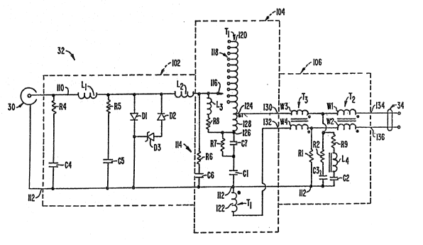
Referring to Figure 2, there is shown a first
preferred embodiment of a matching device 32 in accordance
with the invention. The matching device 32 comprises three
sections, namely a low-pass filter section 102 having a
first or unbalanced port 30, an autotransformer section 1~4
and a common mode current rejection section 106 having a
second or balanced port 34.
The common mode current rejection section 106
provides, simultaneously, d.c. passthrough, high common mode
impedance at signal frequencies (1 MHz to 10 MHz) and at low
to ~id-range frequencies (10 kHz to 500 XHz), and inductive
current cancellation. The autotrans~ormer section 104
provides adjustable impedance matching and unbalanced signal
to balanced signal conversion.
The low-pass filter section 102 provides reliablP
rejection of residual spurious r.f. signals which might be
present at the unbalanced input port 30, as well as
overvoltage protection against the possibility hat
undesired voltage might be present on the balanced side
which could damage delicate circuitry connected to the
unbalanced side.
The low-pass filter section 102 comprises a linear
phase passive L-~ filter comprising a ~irst inductor Ll and
a first capacitor C4 looking into a characteristic resistive
.~
:
.
: '
.
impedance of 50 Ohms at the unbalanced port 30, the
unbalanced port having a center conductor side 110 and a
common node 112. A first resistor R4 set at 50 Ohms in
series with the capacitor C4 across the unbalanced port 30
assures the load impedance at high frequencies remains at
the desired characteristic impedance. A second resistor R5
is provided in series with a second capacitor C5 between the
first inductor L1 and the common node 112. A second
inductor L2 is coupled from the first inductor L1 to a
second port at the autotransformer section 104, terminating
across a fixed high frequency load 114 (resistor R6 and
capacitor C6) and in a primary tap 116. Overvoltage
protection is provided by diodes Dl, D2 and Zener diode D3
from L1 and L2 to the common node 112. The parasitic
capacitance of the diodes contribute to the capacitance
values of the low-pass filter section 102.
The,autotransformer section 104 includes the fixed
high-frequency load 114 of R6 and C6, an autotransformer
coil 118 having a large multiple-tap winding 120 and a
smaller, isolated winding 12~, the large tapped winding
having a first tap 124 at a point relative to a reference
node 126 which has an equal number of turns as the isolated
: winding 122 thereby to define an output portion 128 on a
cen$er conductor side 130 of the common mode current
rejection section 106. The polarity o~ the isolated winding
: 122 matches the polarity of the large winding 120 (as
indicated by polarity dots)O The isolated winding 122 is
coupled at one end to the common node 112 and at the other
end to a signal common side 132 of the common mode current
rejection section 106. The multiple-tap winding 120 has a
plurality of tap connections at for example every turn ~or
connection of the primary tap 116 to the winding 120. The
preferable tap connection increment is to provide an eight
percent change in impedance in order to assure that it is
possible to attain an impedance match within a desired
tolerance for impedance matching of plus or minus four
percent.
~.~856~;~
A doc~ blocking capacitor Cl is provided between
the common node 112 (at the winding 122) and the base 126 of
the output portion 128 through a first compensation resistor
R7. The value of the first compensation resistor R7 is in
the low hundred ohm range. The primary tap 116 is provided
with a coupling through a third inductor ~3 and a second
compensation resistor R8 to the base 126. A high frequency
compensation capacitor C7 is coupled between the base 126
and the blocking capacitor C1 to minimize high frequency
attenuation between the unbalanced port 30 and balanced port
34. The combination of the d.c. blocking capacitor C1 and
the third inductor L3 determines the transition frequency
above which impedance matching occurs. The combination of
the compensation capacitor C7 and compensation resistors R7
and R8 provides damping ~o minimize ringing in response to
step chanyes in applied voltage.
The common mode current rejection section 106
having balanced port 34 on one side and center conductor
side 130 and signal common side 132 has in a first preferred
embodiment a first transformer T2 and a second transformer
T3l the first transformer T2 having a first winding Wl and a
second winding W2. The first winding W1 is coupled to a
first balanced port terminal 134 on the center conductor
side 130 to pass differential signals to the first te~minal
134 of the balanced port 34 connector, and the second
winding W2 is coupled to a second terminal 136 of the
balanced port 34 connector on the signal common side 1~2 to
pass differential signals. The first transformer T2 is for
providing a large common mode impedance at high-range
frequencies above about 1 MHz.
The second transformer T3 has a third winding W3
and a fourth winding W4. The third winding W3 is coupled on
: the center conductor side 130 to the first winding Wl to
pass differential signals to said first winding W1, and the
fourth winding W4 is coupled to the second winding W2 on the
signal common side 132 to pass differential signals to said
second winding W2. The second transformer W3 is for
,, , , , , ~, . . .
85~i23
providing a large common mode impedance at midrange
freguencies between about 10 kHz and about 1 MHz.
A fourth inductor L4 is coupled in series with a
resistor R9 and second d.c. blockin~ capacitor C2 between
the ~enter conductor side of the first winding Wl and the
common node 112 of the unbalanced port 30, the fourth
inductor having an inductance value matched to the
inductance value of the third winding W3, Por diverting
current from the third winding W3 to cancel common mode
offset current in the third winding W3.
Further, the ~o~mon mode current rejection section
106 has a first resistor Rl, a second resistor R2 and a
first coupling capacitor C30 The first resistor R~ is
coupled between the signal co~mon side 132 of said second
winding W2 and the con~non node 112. The second resistor R2 is
coupled between the center conductor side 130 of said first
winding Wl and the common node 112 through the first
coupling capacitor C3 for reducing effPcts o~
capacitively coupled noise from external sources through the
balanced port 34.
Figure 3 illustrates a matching device 32' in
accordance with a -~econd preferred embodiment of the
in~ention. This embodiment differs from the embodiment o~
: Figure 2 in that the second transformer T3 is coupled
between the low-pass filter section 102 and the
autotransformer section, and it would therefore not appear
as an explicit part of the common mode current rejection
section 106. However, its electrical function is exactly
the same as in the embodiment of Figure 2 in t~at it
provides high common mode impedance to midrange freguencies.
: The advantage of placement of the second transformer T3 at
the second port of the low-pass filter section 102 is
two-fold. First, the long length of wire in the transformer
windings, the impedance o~ which is fixed, does not need to
~ 35 change value with chang~ in tap setting of the
:~: autotransformer. Second, the impedance at the second port
of the low-pass filter section 102 is much lower than
.. . . .
.
~28S6;;:3
adjacent the ~irst transformer T2, and as a consequence
standard bifilar magnet wire may be employed for its
windings with ready match to the characteristic impedance of
50 Ohms at the second port.
The invention has now been explained with
reference to specific embodiments. OthPr embodiments will
be apparent to those of ordinary skill in this art.
Therefore, it is not intended that this invention be
limited, except as indicated by the appended claims.
~5
;
~ 30
.
~ 35