Note: Descriptions are shown in the official language in which they were submitted.
ELECTRICAL SOC~OET APPARATUS WITH TEMPORARY HOUSING
BACKÇROUN_D OF THE INVENTION
This invention relates in general to plugs and
soc~ets which are usad for electrical interconnection
purposes. More particularly, the invention relates
to sockets which are mounted on printed circuit
boards and other substrates.
Unfortunately, despite continued e~forts toward
miniaturization, conventional sockets still tend to
consume relatively large amounts of volume in both
the vertical and horizontal dimensions with respect
to the printed circuit boards on which such sockets
are mounted.
BRIEF SUMMARY OF THE INVENTION
onP object of the present invention is to
provide a socket for a printed circuit board or other
substrate which consumes a minimal amount of volume
on the substrate.
Another object of the present invention is to
provide a socket which includes a temporary housing
which can be removed to free-up valuable space on a
printed circuit board or other substrate.
In one embodiment of the invention, a socket is
provided which includes a connector element for
:
., . ~
.
receiving and ma~ing a connection to an electrical
lead. A soluble housing is attached to the connector
element for temporarily housing said connector
element. The housing is removable from the connector
element via solvent once the connector element is
inserted into an aperture in the substrate.
The features of the invention believed to be
novel are specifically set forth in the appended
claims. However, the invention itself, both as to
its structure and method of operation, may best be
understood by referring to the following description
and the accompanying drawings.
BRIEF DESCRIPTION OF 1~ DRAWINGS
FIG. 1 is a representation of a the connector
sockèt of the invention in an early stage of
fabrication.
FIG. 2 is a representation of the conneator
socket of the invention after tooling has bee used to
shape the connector.
FIG. 3 is a representation of the connector
socket of FIG. 2 after a temporary housing has been
~5 applied to the connector.
Fig. 4 is a perspective view of the connector of
the invention shown prior to insertion in an aperture
of a substrate.
Fig. 5 is a representation of several of the
connector sockets of FIG. 3 shown attached to a
common bar or reel.
Fig. 6 is a perspective view of the connector
socket of the invention shown after insertion in an
aperture in a substrate.
FIG. 7 is sectional view of the connector socket
, , , : . ~
- , .~ - .
- . ~ . ,, ' :,
,
:
. . , ~ ~ . ', .
of FIG. 6 along section line A-A' prior to removal of
the temp~rary housing.
FIG. 8 is sectional view of the connector socket
of FIG. 6 along section line A-~' after removal of
the temporary housing.
FIG. 9 is a cutaway perspective view of the
installed socXet with a lead therein.
1~ DE~AILED DESCRIPTION OF THE INVENTION
Turning now to FIG. 1, one connector element
~hich is used in the socket of the present invention
is shown as connector element 10. Connector element
1~ 10 includes a central spine 15 having opposed ends
15~ and 15B and a center 15C. A plurality of arm
pairs 21~-21B, 22A-22B, 23A-23B and 24A-24B extend
radiàlly outward from spine 15 in the region of spine
15 between end 15B and center 15C. Connector element
10 further includes arms 25A and 25B which are each
substantially semi-circularly shaped. One end of
each of arms 25A and 25B is connected to spine 15
between end 15B and center 15C as shown in FIG 1.
Connector element 10 is fabricated from electrically
~5 conductive material by a stamping or metal cutting
process.
As shown in FIG. 2, arm pairs 21A-21B, 22A-22B,
23A-23B and 24A-24B are shaped by appropriate tooling
into the form of semicircles. When so formed, arms
21A, 22A, 23A and 24A face arms 21B, 22B, 23B and
24B, respectively, in a manner which enables the arms
to capture a connector lead therein.
Spine 15 is bent at 30 and 35 to bring the plane
of arm pair 25A-25B substantially parallel with the
plane of the other arm pairs 21A-21B, 22A-22B, 23A-
23B and 24A-24B. An angled portion 40 is thus formed
.
:
in spine 15. The lower portion of spine 15 to which
arm pairs 21A-21B, 22A-22B, 23A-23B and 2~A-24B are
attached is now re~erred to as lower spine 45. The
portion of spine 15 above arm pair 25A-25B is now
referred to as upper spine 50. Upper spine 50 is
bent at 55 where it meets arm pair 25A-25B such that
upper spine 50 is in a plane substantially parallel
with lower spine 45.
FIG. 3 shows the connector socket 60 formed by
attaching a temporary housing 65 to the portion of
connector element 10 below arm pair 25A-25B. Housing
65 is shaped to fit into an aperture 70 in a circuit
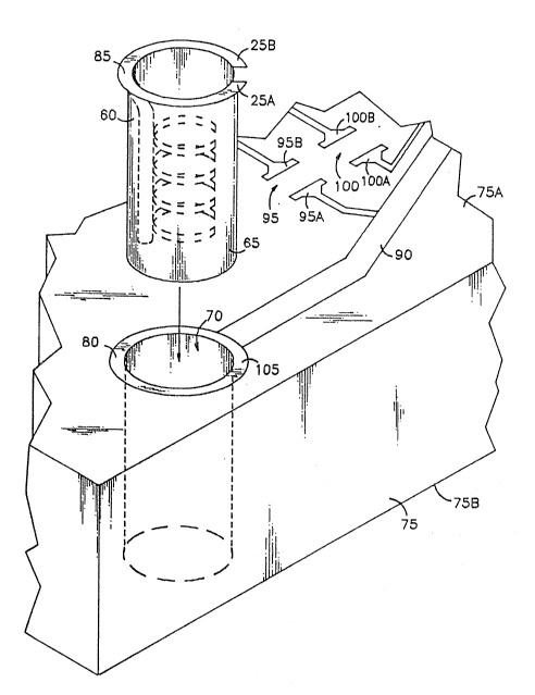
board or other substrate 75 as shown in FIG. 4.
Housing 65 is also shaped to permit an automatic
parts placement machine, that is, a so-called "pick
and place" machine, to pick up socket 60 by gripping
housing 65. That is, housing 6S provides a handle
which an automatic parts placement machine can grip.
In this embodiment of the invention, housing 65
exhibits a cylindrical shape to facilitate placement
in the cylindrical aperture 70 of FIG. 4O
Those skilled in the art will appreciate that the
cylindrical shape of housing 65 is described as an
example and that other geometries for 65 can be
selected for housing 65 as long as the selected
geometry is capable of being gripped by an automatic
parts placement machine, or alternatively, is capable
of being manually handled.
For convenience of use with automatic parts
placement machines, connector sockets 60 are
fabricated in a reel 78 as shown in FI5. 5. That is,
a plurality of sockets 60 are connected to a common
reel 78 by attaching the upper spines 50 of sockets
60 to reel 78 at spaced intervals. The automatic
parts placement machine shears off upper spine 50 at
,: . , : -
.: ,
.. . , ....................... . . :
,; .,
the time of insertion into substrate 75 as shown in
FIG. 4.
Temporary housing 65 is fabricated from a
soluble material, for example TC-561 manufactured by
5 Techform Laboratories, Housing 65 is molded onto the
portion of socket 60 below arm pair 25A-25B.
Alternatively, the portion of socket 60 below arm
pair 25A-25B is conformally coated with soluble
material to form housing 65.
As mentioned brlefly above, FIG, 4 shows a
subst~ate 75 with an aperture 70 into which socket 60
is to be inserted. For purpose of this example, it
will be assumed that substrate 75 is a pxinted
circuit board including opposed surfaces 75A and 75B.
A land or ring 80 of electrically csnductive material
is situated on surface 75A surrounding the opening of
aperture 70 onto surface 75A. Ring 80 is shaped to
mate with arm pair 25A-25B when socket 60 is inserted
into aperture 70. Arm pair 25A-25B forms a rim 85
which supports socket 60 when socket 60 is inserted
into aperture 70.
A conductive runner 90 is shown connected to
ring 80 on surface 75A to illustrate that socket 80
can be connected to other circuit elements on
2~ substrate 75 via such runners. Mounting sites 95
and 100 are also shown on surface 75A for receiving
surface mounted devices thereon. Mounting site 95
includes a pair of conductive lands 95A and 95B for
receiving a surface mounted device. Mounting site
100 also includes conductive lands lOOA and lOOB for
receiving a surface mounted device.
FIG. 4, and 6-9 illustrate the method of
placement of socket 10 in aperture 70 on printed
circuit board 75 and removal of temporary housing 65.
Returning momentarily to FIG. 4, prior to placement
of socket 60 in aperture 70, a layer of solder 105 is
printed or otherwise deposited on ring ~0. At this
time, any other conductive lands on surface 75A are
covered with solder in preparation for later solder
reflow.
Substrate 75 is then populated with socket 60 at
aperture 70 and other surface mounted devices at
sites 95 and 100 as seen in the cutaway perspective
view of FIG. 6. The automatic placement machine
shears upper spine 50 (shown in FIG. 5) from the
remainder of socket 60 prior to insertion of socket
60 into aperture 70. The rim 85 formed by arm pair
25A-25B rests on solder layer 105 which is atop ring
80 as shown in FIG. 7. FIG. 7 is a sectional view of
socket 60 and substrate 75 along section line A-A' of
FIG. 6. Solder layer 105 is more clearly shown in
FIG. 7.
The populated substrate 75 is then subjected to
a solder reflow environment. That is, substrate 75
is inserted into an oven which axhibits a temperature
~0 suf~iciently high to cause the solder on the lands of
substrate 75 and solder layer 105 to melt or reflow.
When reflow occurs, a permanent el~-ctrical connection
is formed between rim 85 and conductive ring 80.
While solder reflow was occurring, temporary housing
65 acted as a shield which prevented solder from
contacting arm pairs 21A-21B, 22A-22B, 23A-23B and
24A-24B. During reflow, permanent electrical
connections are formed between the lands at sites 95
and 100 and respective surface mounted devices .
Temporary housing 65 is removed to expose arm
pairs 21A~21B, 22A-22B! 23A-23B and 24A-24B to make
them accessible for connection purposes. That is,
the populated reflowed substrate 75 is subjected to a
solvent capable of dissolving the particular soluble
material selected for temporary housing 65. For
example, when TC-561 is selected as the soluble
- . , ' ~ . ~ , .
: . ' : . , ' ,
:.
: ' ' - . ,;
` - -
material for temporary housing 65, then warm water is
an example of one solvent which may be selected to
dissolve and remove temporary housing 65. Also by
way of example, when RR-490 manufactured by Lancer
Chemical is selected as the soluble material for
temporary housing 65, then Freon TMS~ manufactured by
DuPont is an example of another solvent which may be
selected to dissolve and remove temporary housing 65
from socket 60. Those skilled in the art will
appreciate that temporary hou~ing material/solvent
combinations other than those given in the examples
above may be employed in practicing the invention.
The populated reflowed substrate 75 is defluxed
to remove flux residues associated with reflow
soldering. This defluxing step i5 accomplished by
subjecting the populated substrate 75 to a defluxing
agent such as Freon TMS~. The invention includes an
embodiment wherein the temporary housing 65 is
fabricated from a material selected to be soluble in
the defluxing agent used to deflux the populated
substrate after solder reflow. In this manner, the
step of defluxing the reflowed substrate 75
simultaneously achieves the dissolving of temporary
housing 65. For example, when temporary housing 60
is fabricated from RR-490, the defluxing agent Freon
TMS~, is used to remove temporary housing 60 and to
deflux the populated reflowed substrate 75.
Alternatively, the removal of temporary housing 65
and the defluxing of reflowed substrate 75 can be
carried out in separate steps if desired. In that
case, the material of temporary housing 65 is
selected to be soluble in a solvent other than the
defluxing agent.
After the reflowed substrate 75 is defluxed and
the temporary housing 65 is removed from socket 60,
socket 60 appears as in the sectional view of FIG. 8.
.
It is seen that arm pairs 21A-21B, 22A-22B, 23A-23B
and 24A-24B are now free to accept a component lead
115 or other lead therein. Such a lead is grasped
between the arms of the respective arm pairs. The
perspective cutaway view of substrate 75 in FIG. 9
more clearly shows arm pairs 21A-21B, 22A-22B,
23A-23B and 24A-24B gripping and making connection to
lead 115 therein.
From the above description, it is clear that
the invention includes a method for installing a
socket having a plug connecting element mounted in a
soluble temporary housing. The socket is installed
in a substrate having at least one aperture for
receiving the socket in accordance with the method
the step of inserting the plug connecting element of
the socket into the aperture. The method further
includes the step of soldering a portion of the plug
connecting element to a conductor on the substrate.
The method includes the step of removing the
~0 temporary housing with an appropriate solvent. An
electrical lead is then inserted into the connecting
element of the socket.
The foregoing has described a soc~et apparatus
for a printed circuit board or other substrate which
consumes a minimal amount of volume on the substrate.
The socket includes a temporary housing which can be
removed to free-up valuable space on the substrate
and adjacent to the substrate.
While only certain preferred features of the
invention have been shown hy way of illustration,
many modifications and changes will occur to those
skilled in the art. For example, the location and
shape of temporary housing 65 is not limited to that
illustrated in the drawings. Temporary housing 65
may be located on socket 60 at locations other than
that show~ as long as housing 65 provides a handle
': . '
: ,
~L21~
which is accessible for an automatic parts placement
machine to grip. Moreover, temporary housing may
exhibit a shape other than that illustrated as long
as the selected shape exhibits sufficient structural
integrity to enable an automatic parts placament
machine to grip housing 65. In addition, the
invention may be practiced with connector elements
other than the particular connector element 10 which
was shown for purposes of example. Those skilled in
the art will appreciate that the temporary soluble
housing or handle described herein may be attached to
many different types of connector elements to enable
such elements to be placed by an automatic parts
placement machine. It is, therefore, to be
understood that the present claims are intended to
cover all such modifications and changes which fall
within the true spirit o~ the invention.
.
:-
,
.~ ~- '........................... .