Language selection

Search

Patent 1286014 Summary

Third-party information liability

Some of the information on this Web page has been provided by external sources. The Government of Canada is not responsible for the accuracy, reliability or currency of the information supplied by external sources. Users wishing to rely upon this information should consult directly with the source of the information. Content provided by external sources is not subject to official languages, privacy and accessibility requirements.

Claims and Abstract availability

Any discrepancies in the text and image of the Claims and Abstract are due to differing posting times. Text of the Claims and Abstract are posted:

  • At the time the application is open to public inspection;
  • At the time of issue of the patent (grant).
(12) Patent: (11) CA 1286014
(21) Application Number: 1286014
(54) English Title: TELEPHONE CONNECTOR WITH BYPASS CAPACITOR
(54) French Title: CONNECTEUR DE TELEPHONE A CONDENSATEUR DE DERIVATION
Status: Term Expired - Post Grant
Bibliographic Data
(51) International Patent Classification (IPC):
  • H01R 13/26 (2006.01)
  • H01R 13/33 (2006.01)
  • H01R 13/658 (2011.01)
  • H01R 13/66 (2006.01)
  • H01R 13/719 (2011.01)
(72) Inventors :
  • TALEND, DONALD RICHARD (United States of America)
(73) Owners :
  • CORCOM, INC.
(71) Applicants :
  • CORCOM, INC. (United States of America)
(74) Agent: SMART & BIGGAR LP
(74) Associate agent:
(45) Issued: 1991-07-09
(22) Filed Date: 1987-08-11
Availability of licence: N/A
Dedicated to the Public: N/A
(25) Language of filing: English

Patent Cooperation Treaty (PCT): No

(30) Application Priority Data:
Application No. Country/Territory Date
901,824 (United States of America) 1986-08-29

Abstracts

English Abstract


ABSTRACT
A modular jack for telephones in which bypass
capacitors have been connected to the leads so as to
bypass noise and other high frequency signals. End
mounted ceramic capacitors extend from the leads to a
ground plane which is provided with flexible fingers
and which is connected to a suitable ground so as to
provide a grounding contact for the capacitors.


Claims

Note: Claims are shown in the official language in which they were submitted.

-6-
CLAIMS
1. A telephone jack comprising an insulating
body member formed with an opening for a mating
connector, a plurality of electrical contacts mounted
in said body member, a plurality of tombstone
capacitors with first ends in contact, respectively,
with said plurality of electrical contacts, an
electrically conducting planar member mounted to said
body member and formed with a plurality of flexible
fingers, respectively, engaged by the second end of
said plurality of tombstone capacitors, and means for
grounding said electrically conducting planar member.
2. A telephone jack according to claim 1
including an electrically conducting cover member
mounted to said body member over said electrically
conducting planar member and electrically connected to
said planar member.
3. A telephone jack according to claim 2
wherein said plurality of tombstone capacitors are
mounted so that their longitudinal axes extend parallel
to each other.
4. A telephone jack according to claim 3
wherein said electrically conducting planar member is
soldered to said electrically conducting cover member.
5. A telephone jack according to claim 3
including an electrically insulating member formed with
a plurality of holes in which said plurality of
tombstone capacitors are respectively mounted and said
insulating member mounted between said cover member and
said plurality of electrical contacts.
6. A telephone jack according to claim 5
including a printed circuit board formed with at least
one mounting opening, and said body member formed with
at least one mounting prong which is receivable through
said mounting opening to attach said telephone jack to

-7-
said printed circuit board and said plurality of
electrical contacts connected to circuit paths on said
printed circuit board.
7. A telephone jack according to claim 3
wherein said plurality of electrical contacts formed
with enlarged regions and said first ends of said
plurality of tombstone capacitors, respectively,
engaging said enlarged regions.
8. A telephone jack according to claim 6
including a conductive grounding area formed on said
printed circuit board and at least one electrically
conducting tab extending between said conductive
grounding area and said electrically conducting cover
member.
9. A telephone jack according to claim 6
including an electrically conductive planar plate in
electrical contact with said electrically conducting
cover member.

Description

Note: Descriptions are shown in the official language in which they were submitted.


--1--
TELEPHONE CONNECTOR WITH BYPASS CAPACITOR
.
DESCRIPTION
7 _ . _
This invention relates in general to
electrical contacts in jacks and in particular to a
novel modular telephone jack in which the contacts are
provided with bypass capacitors.
Standard modular telephone jacks are provided
with a number of electrical contacts such as six, eight
or more which make mating engagement with a male
ln contact which is received therein. Such prior art
jacks do not provide bypass capacitors to a ground
plane from the various contacts.
It is an object of the present invention to
provide end mounted ceramic capacitors which extend
between the contacts and a ground plane of the jack.
It is an object of the present invention to
provide a telephone female terminal in which the
various contactors of the terminal are provided with an
enlarged portion upon which are mounted monolithic
~0 surface mounted capacitors which extend to a ground
plane which is connected to a ground plane of a printed
circuit board or to another suitable grounding region.
Metal springs are provided which engage the
ends of the capacitors which provide for mechanical
~5 cushionin~ of the capacitors and for alignment.
other objects, features and advantages of the
invention will be readily apparent from the following
description of certain preferred emhodiments thereof
taken in conjunction with the accompanying drawings,
although variations and modifications may be effected
without departing from the spirit and scope of the
novel concept of the disclosure and in which:
ON`~E DR~WINGS
.
FIG. 1 is a front plan view of the novel
3s connector of this invention;
.:,- ~ ', .,
.

~2 ~
--2--
FIG. 2 is a sectional view taken on line II-II
from FIG. l;
FIG. 3 iS a top plane view of the invention
with portions removed;
FIG. 4 is a cut-away top view of the
invention;
FIG. 5 is a partial ~iew illustrating the
connector prongs and contacts;
FIG. 6 illustrates a modification of the
1~ invention
FIG. 7 is a sectional view taken on line VII-
VII from FIG. 6;
FIG. 8 is a top plan view with portions
removed; and
FIG. 9 iS a break-away top view of the
invention.
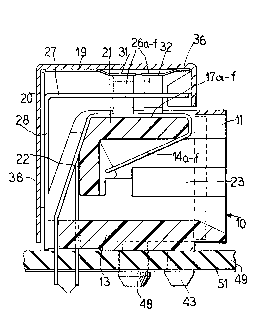
FIGS. 1-5 illustrate a first embodiment of the
invention which comprises a terminal 10 formed with a
plastic body member 11 in which a jack receiving hole
23 is formed in a front face thereof. The plastic
member as shown in the sectional view of FIG. 2 has a
bottom member 13 and a top member 21 and a back portion
~ plurality of electrical contact members 14a
through 14f have first portions which extend into the
openin~ 23 so as to make electrical contact with mating
terminals on a male plug received in the openinq 23 and
l~ave top portions 17a which pass over the top 21 of the
plastic member 11 and are formed with enlarged
capacitor contacts 18a through 18f in the top portions
30 17a through 17f of the contact which are offset .
relative to each other as illustrated in FIG. 3. The
rear portions of the contacts 14a through 14f pass down
beyond the rear portion 22 of the plastic member 11 and
extend through the bottom portion 13 of the plastic
member 11 and through a printed circuit board 49 which
'~, ' ' . ~ . ......... '- '' ,:
.
' '
,' , .. :' ,. :, ' ',

is provided with printed circuit contact area 51 to
make electrical contact with the ends 16a through 16f
of the contacts 14a through 14f as illustrated in FIGS.
1 and 2, for example.
~ounting prongs 47 and 48 pass through aligned
openings in the printed circuit board 49 for mounting
~lle female contact 10 on the board 49. A pluralit~ of
end mounted capacitors 26a through 26f extend through
an insulating sheet 27 which has a rear portion 28
1~ which is mounted relative to the plastic housing 11
such that first ends of the capacitors 26a through 26f
engage the electrical contact regions 18a through 18f
of the electrical contacts 14a through 14f.
A planar member 19 is formed with downwardly
1~ bent fingers such as 31 and 32 illustrated in FIGS. 2
and 4 which engage the second ends of the tombstone
~apacitors 26a through 26f and the member 19 is
electricall~ connected to a conductive core 36.
downwardly extending portion 20 of cover 36 is mounted
between downwardly extending portion 28 of the
insulating member 27 and the rear 38 of the electrical
conducting cover member 36. The member 19 may be
soldared to the cover member 36 by providing solder
through holes 37 formed in the finger member 19 as
illustrate3 in FIG. 4.
The cover member 36 is formed with sides 39
and 41 and grounding tabs 42 and 43 which extend from
the cover member 36 through openings formed in the
printed circuit board 4g and make electrical contact
with grounding regions on the printed circuit 51 so as
to ground the upper ends of the capacitors 26a through
26f through the fingers 31 and 32, the finger member 19
and the cover member 36~
In use, the terminal 10 is mounted on a
printed circuit board 49 with contacts 16a through 16f
: ' . - ~ '
,

which extend through board 49 electrically connected to
different terminals on the printed circuit paths 51.
The other ends of the capacitors 26a through 26f are
grounded through the grounding tabs 42 and 43 which are
connected to the side walls 39 and 41 of the
electrically conducting cover member 36. The male
member of the connector is inserted into the opening 23
to make electrical connection between the terminals 14a
through 14f and such contacts are grounded through
capacitors 26a through 26f. As illustrated in FIG. 5,
the cover member side walls 39 and 41 are provided with
tabs 46 which are deflected into mating opening formed
in the plastic member 11 to firmly attach the cover
member 36 to the plastic body member 11.
FIGS. 6-9 illustrate a second embodiment of
the invention wherein grounding is made to a front
grounding plate rather than to the printed circuit
board 49.
FIGS. 6-9 illustrate a modification of the
invention wherein the grounding arrangement has been
changed. This merely requires the modification of the
cover member and the plastic bod~ member. In this
embodiment, the cover member 136 has a front portion
152 which is connected to a conductive planar member
~5 151 by solder 153. The plastic member 111 has a front
rim 154 behind which the electrical conductive planar
member 151 fits as shown in FIGS. 7, 8 and 9. The
terminals 14a through 14f, the insulating plate 27, the
capacitors 26 have the same configuration as that of
the first embodiment. The cover member 136 is modified
so as to eliminate the extension tabs 42 and 43 which
are used for grounding in the embodiment illustrated in
FIGS. 1-5 and grounding occurs through the plate 151
which is connected by the solder 153 to cover member
35 136. This embodiment allows mounting and grounding to

~2~
conductive back panel.
Although the invention has been shown with six
electrical terminals, it is to be realized that it may
be modified to any desired number such as 8 or 10, for
example. Item 12 of FIG. 3 (flangeless) could be
modified as item 154 of FIG. 8 (flanged) with or
without 151 conductive mounting member.
Although the invention has been described with
respect to preferred embodiments, it is not to be so
1~ limited as changes and modifications can be made which
are within the full intended scope of the invention as
deEined by the appended claims.
. ~:, ';, : . ' ,
: . ,, . . :
. . :

Representative Drawing
A single figure which represents the drawing illustrating the invention.
Administrative Status

2024-08-01:As part of the Next Generation Patents (NGP) transition, the Canadian Patents Database (CPD) now contains a more detailed Event History, which replicates the Event Log of our new back-office solution.

Please note that "Inactive:" events refers to events no longer in use in our new back-office solution.

For a clearer understanding of the status of the application/patent presented on this page, the site Disclaimer , as well as the definitions for Patent , Event History , Maintenance Fee  and Payment History  should be consulted.

Event History

Description Date
Inactive: IPC from PCS 2022-09-10
Inactive: IPC expired 2011-01-01
Inactive: Expired (old Act Patent) latest possible expiry date 2008-07-09
Inactive: IPC from MCD 2006-03-11
Letter Sent 2004-07-22
Inactive: Late MF processed 1999-04-29
Letter Sent 1998-07-09
Grant by Issuance 1991-07-09

Abandonment History

There is no abandonment history.

Owners on Record

Note: Records showing the ownership history in alphabetical order.

Current Owners on Record
CORCOM, INC.
Past Owners on Record
DONALD RICHARD TALEND
Past Owners that do not appear in the "Owners on Record" listing will appear in other documentation within the application.
Documents

To view selected files, please enter reCAPTCHA code :


To view images, click a link in the Document Description column. To download the documents, select one or more checkboxes in the first column and then click the "Download Selected in PDF format (Zip Archive)" or the "Download Selected as Single PDF" button.

List of published and non-published patent-specific documents on the CPD .

If you have any difficulty accessing content, you can call the Client Service Centre at 1-866-997-1936 or send them an e-mail at CIPO Client Service Centre.


Document
Description 
Date
(yyyy-mm-dd) 
Number of pages   Size of Image (KB) 
Cover Page 1993-10-21 1 13
Drawings 1993-10-21 2 85
Abstract 1993-10-21 1 10
Claims 1993-10-21 2 60
Descriptions 1993-10-21 5 168
Representative drawing 2000-07-06 1 14
Maintenance Fee Notice 1998-08-06 1 179
Late Payment Acknowledgement 1999-05-17 1 172
Fees 1999-04-29 2 66
Correspondence 2004-07-22 1 9
Fees 1994-06-06 1 41
Fees 1996-04-30 1 38
Fees 1993-05-11 1 26
Fees 1995-06-20 1 43