Note: Descriptions are shown in the official language in which they were submitted.
~363~i~
Title of the Invention: HIGH SPEED HYBRID DIGITAL DRIVER
FIELD OF THE INVENTION
The present invention relates to digital drivers, and
more particularly to such a driver capable of translating
digital signals to different voltage levels in accordance
with programmed reference inputs.
BACKGROUND OF THE INVENTION
Military facilities, including shipboard electronic
instrumentation, require frequent testing and calibration
in order to operate reliably. Efforts have been made in
recent years to develop a eingle testing apparatus which
i8 capable of testing a wide variety of electronic
devices. The advantage to such an approach is to avoid
the cost and inconvenience of having individual test
equipment for electronic devices to be tested.
Generally, such test apparatus, known as automatic
test equipment (ATE), will provide a parallel digital
output to a device or unit undergoing test (W T). ~s test
data is generated by the automatic test eguipment, the
response of a connected W T is detected and compared to an
expected response. Failure to respond properly uncovers a
fault with the W T.
The problem with available prior art test equipment
is a relatively low operating speed and the lack of
conveniently testing the capability of a UUT to operate in
a tri-state condition.
BRIEF DESCRIPTION OF THE PRESENT INVENTION
The present invention offers a high-speed hybrid
digital driver which interfaces TTL digital word
generators (DWG) with W T's.
The present invention provides capability of
converting the DWG signals which are TTL level signals
into signals whose upper and lower voltage levels are
:~X~ iS
programmable. The timing is provided by the DWG. That
is, the present invention does not modify the duration of
the "ONES" and "ZEROS." However, the amplitude of the
ONE and likewise the amplitude of the ZERO are provided
as reference voltages to the driver. Thus, the needs of
a UUT for special levels of digital signals can be
satisfied. In addition, the driver also provides
additional driving power beyond that available from the
TTL output chip in the DWG itself.
Further, the present driver includes a control
input which allows the driver output to be put into a
tri-state mode, independent of the state of the signal
input.
Accordingly, the present high speed digital driver
offers the user great versatility and enables a large
variety of UUTIs to be fully tested by a single ATE.
BRIEF DESCRIPTION OF THE FIGURES
The above-mentioned objects and advantages of the
present invention will be more clearly understood when
considered in conjunction with the accompanying drawings,
in which:
FIG. l is a block diagram of the present high
speed digital driver which interfaces between a digital
word generator and a unit undergoing test; and
FIG. 2 is a schematic view of a first channel of
the driver circuit.
DETAILED DESCRIPTION OF THE INVENTION
FIG. 1 illustrates a basic block diagram of the
present invention.
The presence of an automatic test equipment (ATE)
is indicated by reference numeral 8. This ATE 8 is
conventional; and briefly, it generates logic patterns or
data words which are to be transmitted to the input of a
unit undergoing test (UUT) ll. Since each type of W T
.. ,. " , '
.
- - -
. -
-
1~363~i~5
generally requires diffarent logic patterns to complete atest, the ~TE 8 is microprocessor based in order to
generate the necessary logic patterns in the form of
digital words, depending upon the particular W T 11 being
tested. Within a conventional ATE 8, a plurality of
digital word generators (DWG) 9 is provided to generate
digital words in simulation of the logic pattern to be
input to the W T 11. If a parallel output is provided by
an ATE 8, a separate DWG 9 must be provided for each of
the parallel outputs. Otherwise stated, since the ATE 8
generates a data word comprised of a number of bits, a
separate DWG 9 is provided for each bit.
The hybrid circuitry shown connected between the
output of DWG 9 and the input of UUT 11 serves to
translate the logic levels generated by the DWG 9 and
presents such translated levels to the input of UUT
11, as is required by the latter unit in order to complete
a test. As previously mentioned, different types of W T's
11 will require inputs of different binary levels. Thus,
the present invention must be capable of generating
selectable input levels for the W T 11. Other than this
selectable level change, the driver of the present
invention is not intended to change the pulse width or
shape of the single bit signal provided at the DWG 9.
With this brief introduction to the invention,
further reference i8 made to FIG. 1 wherein the signal
flow through the driver circuit of the invention will now
be discussed.
The signal from the DWG 9 appears as an input to
a gate network 16. In the event the tri-state control
line 14 does not carry a control signal from DWG 9, the
signal at input line 10 will pass to upper and lower
paths 18 and 20 of the driver to translate the voltage
levels from the DWG 9 to selectable levels for the W T
11, as will be presently explained. However, in the
event that the DWG 9 does generate a tri-state control
- ' '. ' :, .
' , . '
,'..... ', :,, ' ' ' ' '
6365
signal on line 14, the gate network 16 will open, thereby
conditioning the driver output 12 to enter a tri-state
mode for the UUT 11. As is known by those skilled in the
art, such a tri-state mode at the input of the UUT is
accompanied by a high impedance, no signal condition.
The present driver circuitry simulates such a tri-state
mode, regardless of the high speed signal appearing on
line lO. Considering the upper or high level signal
path 18, the signal on line 10 passes through the gate
network 16 to input 19 of level shifter 22. The level
shifter converts conventional TTL low logic levels from
the DWG 9 to a more acceptable level to be utilized by a
typical UUT 11. The output from level shifter 22 is
connected with the input of a transistor switch 26 which
will open and close in accordance with the high binary
levels of the original input signal on line lO.
An important aspect of the present invention is
that the output of switch 26 has a selectable amplitude
in accordance with a high reference voltage at terminal
28 connected to another input 30 of switch 26 via a load
sense resistor 32. By varying the voltage at 28, the
high level of the original input signal will be
correspondingly altered at the driver circuit output 12,
connected to the input of the UUT 11. In a preferred
embodiment of the present invention, the high level
voltage at 28 i5 programmed by a computer (not shown) in
accordance with the particular W T 11 being tested.
Short circuit protection through the driver is
provided by an overload detector 34 having its input
connected across the load resistor 32. The output from
detector 34 is connected at a second input 36 of level
shifter 22 so that the occurrence of an overload
condition, as sensed across resistor 32, opens the
circuit path through level shifter 22 thereby preventing
component destruction.
.
. . .
. '. ' ',, ' . . .
;36~5
The lower signal path for the digital word provided
to UUT 11 at dri~er output 12 is generally indicated by
reference numeral 20 and is seen to include the same type
of level shifter 38, switch 40, and overload detector 44
as was present in connection with the upper signal path
18. In order to properly select the low level of the
signal input to W T 11, a programmable low level voltage
is introduced to the driver circuit at 42.
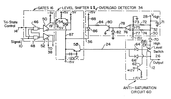
FIG. 2 is an elaboration of the driver circuitry
which has been explained in connection with FIG. 1. The
reference numerals are the same for similar components
indicated in the figures. The gate network 16 is seen to
include parallel connected gates 46 and 48 which
respectively drive inverters 50 and 52. The output from
inverter 50 drives the high level shifter 22, while the
inverter 52 drives the low level shifter 38. The level
shifter 22 is seen to include transistors 54 and 56
having their emitters connected in parallel. The
collector of transistor 56 drives transistor 58 which
produces the level shifted pulses from the original
signal on input line 10. The level shifted pulses are
then transmitted, along line 24, to a high voltage level
transistor switch 26 via a circuit 60 which prevents
saturation of transistor switch 26. The anti-saturation
circuit 60 iB of conventional design and includes diodes
64, 66, 68 and transistor 62 connected across the
terminals of the transistor switch 26. The programmable
and selectable high input voltage at terminal 28 drives
the emitter of transistor switch 26 via diode 70, the
latter ensuring proper voltage polarity at the emitter of
the transistor switch 26. The collector of the transistor
serves as the output of the driver circuit; then, as shown
in FIG. 1, it is connected to a W T 11. The inclusion of
capacitor 71 across terminal 28 ensures a bypass route for
spurious noise.
- ~ .
- . . : . - -- , :
: . . . , , ~ .
., , ~ ............ .
.
'' ,
.
~286;~6S
The overload detector 34 is shown in greater detail
in FIG. 2. The load resistor 32 is seen to drive the
inputs of an operational amplifier 76 via input resistors
72 and 74 which are connected across capacitor 75 and
respective input parallel grounded resistors 73 and 77.
Utilization of these latter-discussed resistors and
capacitor filter undesirable noise from the input of
the operational amplifier 76. In the event a short
circuit or overload condition is detected by virtue of
an inordinately high voltage across resistor 32, output
current from the operational amplifier 76 generates a
voltage across resistor 78 which is grounded, via diode
82. This developed voltage is then amplified by
transistor 80 and transistor load resistor 84. Transistor
80 is collector biased via resistor 88. When an overload
signal is generated at the output of transistor 80, it is
communicated, via diode 86, to lead 87 in connecting level
shi~ter transistors 56 and 58. In such a circumstance,
the current path through the level shifter 22 is
interrupted until the overload or short circuit condition
is changed.
By virtue of the previous description, the present
invention is seen to offer a high speed hybrid digital
driver which is capable of generating selectable voltage
levels for a UUT 11; and upon generation of a proper
tri-state control signal at 14, the driver will enter a
tri-state mode and appear as a high impedance
non-communicating connection to the input of a W T during
portions o~ a test when a tri-state input to the UUT 11
is desired.
Responses by the UUT 11 are customarily input to
a CPU (not shown) for analysis which, per se, does not
form part of the present invention.
It should be understood that the invention is
not limited to the exact details of construction shown and
' ~' ' ' ~ ',
: ' ', , ' '
' , .',
. . , ' . .
.' . , ' . ,
'~ . :
6~6~;
described herein, for obvious modifications will occur to
persons skilled in the art.
.. . .
-
. .
.
,