Note: Descriptions are shown in the official language in which they were submitted.
lX~ S
Meafiuring ~ ~s
~echnical Fi~l~
The present invention relates generally to
measuring AC current and more particularly to a method
of and apparatus for measuring AC current by
compensating for a DC magnetic flux bias introduced
into a magnetic core of a current transformer as a
function of asymmetric flux properties of the core
resulting from DC being superimposed on the AC current
being monitored.
~ackground ~L~
Current transformers are frequently employed to
monitor power line AC current level. The current
transformer usually includes a magnetic core having a
relatively high magnetic permeability and a primary
winding coupled to a line being monitored. A multi-
turn secondary winding is wound on the core to drive
relatively high impedance circuitry that does not
substantially load the primary winding. Such
structures are used to monitor current for current
measuring purposes, as well as to assist in determining
real and reactive power, and to drive watt hour meters.
In some situations, a DC level is imposed on the
primary winding of the current transformer. For
example, half wave rectifiers are sometimes connected
directly in the primary winding in attempts to defeat
the accuracy of the current measurement. In other
instances, DC rectification loads are connected to the
' . '
.2~63
-- 2 --
line and coupled to the current transformer primary
winding.
The DC level in the primary winding biases the
high permeability magnetic core in one direction, so
that the core has a tendency to become saturated to a
greater extent during half cycles of one polaeity than
during half cycles of the other polarity. Even if the
core is not driven into saturation during half cycles
of either polarity, the amplitude of the voltage
induced in the secondary winding differs during
opposite polarity half cycles with a core having a DC
bias superimposed thereon.
I am awaee of two different prior techniques for
detecting the asymmetric responses during opposite
polarity half cycles of a current transformer secondary
winding having a primary winding sub~ected to a DC
level. In the first technique, referred to as
differential peak detection, a derived control signal
has an amplitude dependent upon the difference in
positive and negative peaks of the secondary current.
In the second, zero crossing detection technique, the
control signal has an amplitude dependent upon the
differential duration of the positive and negative half
cycles of a replica of the current in the secondary
~ 25 winding. The control signal is derived as a DC voltage
; which is applied to a compensating winding wound on the
current transformer. Ideally, the DC current applied
to the compensa~ing winding tends to restore the DC
magnetic flux of the transformer core to the same level
30 it would have had if no DC were imposed on the primary
winding of the transformer.
;~ The differential peak detection technique, as
exemplified by Milkovic, United States Patent
O~ 4,255,705~ is not always effective because transient
, ~ , - ~.; ,.
. - , - . ~ - '
,: . . . ' ' .
. .. - . : .
. .: -. ' : : .
.
1~ ~ 6 3 ~ f i
-- 3 --
effects in the transformer affect the core magnetizing
inductance. If, e.g., a positive half wave rectified
current is applied to the current transformer, the
secondary voltage has positive and negative peaks with
similar magnitudes. The magnitudes are about the same
becau~e the primary winding half wave rectified
positive current is converted into an AC secondary
voltage waveform having a first segment that resembles
a half wave rectified sine wave and a second segment
including a negative peak followed by an exp~nential
ramp. When the primary winding current initially goes
positive at the beginning of a positive sinusoidal half
cycle of the rectified current, the secondary winding
output voltage is negative. The secondary voltage then
increases to a positive peak value, which occurs
approximately simultaneously with the peak value of the
primary winding current. In response to the primary
winding current returning to zero, the secondary
winding voltage drops suddenly to a negative peak value
which is approximately equal to the secondary positive
peak value. The exponential ramp of the second segment
then is derived until the primary winding starts to go
through another sinusoidal half cycle. The first and
second segments occur while the primary half wave
rectified current has finite and zero values,
respectively.
The differential peak detection technique is
subject to significant errors because the positive and
negative peak values have approximately the same
amplitude for the frequently encountered situation of a
half wave rectified sine wave current applied to the
current transformer. Very large percentage errors
occur when two values having approximately the same
amplitude are compared. Hen~e, the differential peak
: ' :
.
. . - - ,
' ' ' ~ . ~
1~3636~
detection technique is subject to inaccuracies which
cannot be tolerated in a high probability situation.
The zero crossing detection technique is subject
to inaccuracies if the amplitudes of a sinusoidal
waveform and a half wave rectified sinusoidal waveform
simultaneously applied to the primary winding are
approximately the same. If, e.g., a sinusoidal
waveform having the same amplitude as a half wave
rectified waveform is applied to the current
transformer primary, the difference in zero crossing
periods of the half secondary winding current is
reduced approximately by a factor of two.
Disclosure of Invention
It is a general object of the present invention to
provide an apparatus for compensating for DC current
flowing in a primary winding of a transformer having
a secondary winding.
This and other objects of the present invention are
attained, in accordance with one aspect of the
invention, by an~apparatus for compensating for DC
current flowing in a primary winding of a transformer
having a secondary winding and a magnetic core with a
B-H curve, the DC current having a tendency to supply
DC magnetic flux to the core to bias the core so as
operating point thereof is displaced from a zero flux
position on the B-H curve thereby to cause positive
and negative current components in the secondary
winding to have different amplitudes and different
time durations, the apparatus comprising means
responsive to the positive and negative current
components for deriving a first signal having a value
determined by the average values of the positive
,. . .
,, ~ .
- - : -
.:
.
'
.
636fi
current components, a second signal having a value
determined by the average values of the negative
current components, and a third signal having a value
determined by a comparison of the amplitudes of the
first and second values to indicate the average values
of the positive and negative components, and means for
controlling the DC magnetic flux supplied to said core
in response to the third signal to overcome the
tendency of the core to be biased away from the zero
flux position.
Brief Descri~tion of Drawina
Fig. 1 is a circuit diagram of a first preferred
embodiment of the invention;
Figs. 2 and 3 are waveforms useful for describing
the operation of the circuit of Fig. 1;
t~
,~ .
, - : . , .
. ~ - ' ,'.~ : ' '
, - ~ ::
. ' ' . ' ' - , . -
1 ~ ~
1~ 8~
Fig. 4 is a circuit diagram of a second embodiment
of the invention; and
Figs. 5a-Sd are waveforms useful in describing the
operation of the circuit illustrated in ~ig. 4.
~s~ MQ~ fQL Carrying Q~ ~h~ iQn
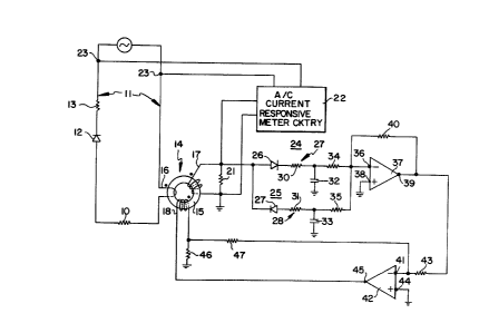
Reference is now made to Fig. 1 of the drawing
wherein a preferred embodiment of the present invention
i8 illustrated in combination with AC power line 11,
such as a 120 volt, 60 Hz power line. Power line ll is
connected to a half wave rectifier including diode 12
and resistor 13, both series connected with the line.
The half wave rectifier is connected to line 11 by a
customer using the line or is part of an impedance load
on the line. In any event, the half wave rectifier
causes the current flowing in line ll to be transformed
from the usual sinusoidal waveform to a half wave
rectified waveform, including positive sinusoidal-like
half cycles having a single polarity, separated by zero
valued half cycles. The half wave rectified sine wave
includes a substantial DC component, as well as a
fundamental component at the power line frequency and
harmonics of the fundamental.
To derive a signal having a magnitude directly
proportional to the AC current components in power line
ll, the power line forms a primary winding of current
transformer 14 including high magnetic permeability
magnetic core 15. Typically, power line ll may be
looped as a single turn 16 through core 15. For many
practical situations wherein a consumer is supplied
with a so-called two phase, three wire power line, a
line from each phase is looped through the magnetic
core. To simplify the exposition, only a single phase
AC line is described in connection with Fig. l.
, . " i ,i ~ b 'i " 'i
. . .' ' ' ,' . , '
,
'~ '," ' '.' ' '' ' ' ' .
1;~8~
Transformer 14 includes multi-turn secondary
winding 17 and auxillary, multi-turn winding 18, both
wound on magnetic core 15. Typically, windings 17 and
18 have an equal number of turns, such as 1000, and the
winding directions of the turns are as indicated in
Fig. 1 by the dot convention so that the polarities oE
the voltages across turns 16 and 17 are the same and
oppositely directed magnetic fluxes are introduced by
windings 16 and 18 in core 15.
Shunting winding 17 is burden or load resistor 21,
having opposite te~minals connected to opposite
polarity input terminals of AC current responsive meter
circuit 22; one terminal of resistor 21 is grounded.
Circuit 22 is typically an electronic watt hour meter
responsive to the AC current in secondary winding 17
and the magnitude of the AC voltage across terminals 23
of AC line 11. Alternatively, circuit 22 responds to
the voltaqes across resistor 21 and terminals 23 to
derive an indication of the instantaneous real or
reactive power supplied by the AC line to load 10, or
is responsive only to the current flowing in line 11.
The impedances of resistor 21 and circuit 22 are such
that they insignificantly load winding 16 and the
voltage across the resistor is a replica of the current
flowing in winding 17.
The DC component of the current in line 11
displaces the quiscent operating point of core 15 from
the normal zero flux value on the B-H hysteresis curve
of the core. The DC current flowing in line 11 and
winding 16 causes core 15 to be biased in a positive or
negative direction. The DC magnetic bias of core 15
causes the AC voltage induced in winding 17 to have
asymmetrical opposite polarity half cycles. The
asymmetry of the opposite polarity half cycles iæ
.~ ~","i~, .~
. . .
.~ . ,~ ' .
.' - :: ~ ' - . '.
.
'-.'' ' ~ ' .
363~;~
~ .
applicable to the amplitude and duration of the current
in secondary winding 17 for the opposite polarity half
cycles.
In certain situations, the amplitude of the
current in line 11 is sufficiently great to cause core
15 to be saturated during opposite polarity half cycles
of the current in line 11. The D~ bias imposed by the
half wave rectifier on the current in line 11 is such
that the degree of saturation for one polarity half
cycle is greater than the degree of saturation during
the other half cycle.
Even if core 15 i8 not saturated, the amplitude
and duration of the cuerent in secondary winding 17
dlffer as a result of the DC flux bias. The embodiment
of Fig. 1 relies upon the difference in the duration
and amplitude of the opposite polarity half cycles to
derive a correction signal having a magnitude
sufficient to overcome the bias effects introduced by
the DC current component in winding 16. The correction
signal determines the amplitude of a DC current applied
to auxillary winding 18. The level of the DC current
applied to winding 18 is controlled to provide the
desired co~pensation.
To provide a measure of the difference in
amplitude and duration of the opposite polarity half
cycles in secondary winding 17, the voltage across
burden resistor 21 is applied to positive and negative
detectlng channels 24 and 25. Detecting channels 24
and 25 are respectively responsive to the positive and
negative voltages developed across burden resistor 21.
To these ends, channels 24 and 25 include silicon
di~odes 26 and 27, respectively having an anade and
cathode ~connected to the ungrounded terminal of
resistor 21. The cathode of diode 26 and the anode of
:
"
:': , ' . ,: ~ '' , - ' --
-- .
'~ ~ j ', . - , .
, . . . .
636fi
10 -,
diode 27 are respectively connected to low pass or
averaging circuits 28 and 29. Circuits 28 and 29
respectively include series resistors 30, 31 and shunt
capacitors 32, 33. The values of resistors 30, 31 and
5 capacitors 32, 33 are selected so the time constants of
averaging circuits 28 and 29 are considerably in excess
of one cycle (more than ten times) of the fundamental
of the AC current flowing in line 11.
The voltages across capacitors 32, 33 respectively
10 represent the amplitudes and durations of tbe positive
and negative voltage components developed across burden
resistor 21. During positive half cycles of the
current flowing in winding 17, current flows through
dlode 26 to capacitor 32 when the voltage across
lS resistor 21 is greater than the sum o~ the 0.6 volt
drop across diode 26 and the voltage across capacitor
32. During negative half cycles of the current flowing
in winding 17, capacitor 33 i8 charged in response to
current flowing through diode 27 when the 0.6 volt drop
20 across the diode and the voltage across capacitor 33
exceeds the voltage across winding 17.
The voltages developed across capacitors 32, 33
are constantly discharged. Capacitors 32, 33 are
connected by resistors 34, 35 to inverting input
25 terminal 36 of DC operational, summing amplifier 37,
having grounded non-inverting input terminal 38.
Connected between output terminal 39 and inverting
input terminal 36 of amplifier 37 is feedback resistor
40. Amplifier 37 and the circuitry associated
30 therewith cause inverting input terminal 36 of the
amplifier to be at virtual ground potential. Current
continuously flows from capacitors 32, 33 through
resistors 34, 35 to the virtual ground potentialA~`~
inverting input terminal 36. The extent of current
. lt,~
. : :
; '
12~36;~
.
1~
flow through resistors 34, 35 is sufficiently great to
cause current to flow through diodes 26 and 27 during
each positive and negative half cycle of the AC voltage
across winding 17.
As described in greater detail inf~, with
reference to Fig. 2, amplifier 37 generates a nc
voltage at terminal 39 which provides a measure of the
differential amplitude and duration of opposite
polarity half cycles of the AC current induced in
secondary winding 17. If line 11 only conducts AC
current, there is a zero DC voltage derived at terminal
39. By connecting diode 12 and resistor 13 in line 11
in the manner indicated, the voltage derived at
terminal 39 has an amplitude and polarity indicative of
the difference in amplitude and duration of the
positive half cycles of the AC current induced in
winding 17 in response to the half wave rectified
current in winding 16.
The DC control signal at output terminal 39 of
amplifier 37 is applied to inverting input terminal 41
of DC current driver or amplifier 42 by way of coupling
resistor 43. Driver 42 includes grounded non-inverting
input terminal 44 and output terminal 45, connected to
one end of winding 18. The other end of winding 18 is
connected to shunt resistor 46 and to feedback resistor
47, con~ected to inverting input terminal 41. The
value of resistor 46, which controls the amount of
current flowing in winding 18, is selected so that the
proper current flows in winding 18 to provide the
desired compensation flux for core 15.
The current flowing through winding 18, as
determined by the output of amplifier 42 and the values
of resistors 46 and 47 as well as the number of turns
in windings 16 ind 18 is such that t~é~ number of ampere
. .
- - ,
.
' ~ :
i6
turns supplied by winding 18 to core 15 is equal to the
number of ampere turns supplied to the core by winding
16. Since the DC fluxes coupled by windings 16 and 18
to core 15 by windings 16 and 18 are equal and the
direction of current flow in the windings is opposite
to each other the DC magnetic flux coupled to the core
15 by winding 16 is cancelled by the DC magnetic flux
coupled to the core by winding 18. Thereby, by proper
selection of resistor 46 the circuit of the present
invention can be used with many different magnetic
cores, while maintaining the number of turns in
windings 17 and 18 the same for different types of
cores.
The current flowing in auxillary winding 18
controls the magnetic flux in core 15 to tend to center
the opeeating point of the magnetic core at the zero
Plux value. Hence, the product of current and time
during wh~ch current flows to capacitor 32 during the
positive half cycles of the voltage across resistor 21
has a tendency to equal the product of current and time
during which current flows to capacitor 33 during the
negative half cycles of the current flowing through
resistor 21. Because (1) capacitors 32, 33 have the
same values, ~2) charging resi~tors 30, 31 have the
same value, (3) the capacitors are connected through
equal valued discharge resistors 34, 35 to virtual
ground and (4) diodes 26 and 27 have virtually the same
voltage drop and impedance when conducting, the
voltages across capacitors 31 of networks 28 and 29
indicate the duration of the time while the opposite
polarity voltages exceed the diode drops and the
maximum amplitudes of the voltages during the opposite
polarity half cycles.
~p,~ ,~, , U`.1~ ~f.` ''
'
,
.
-
,: , ' ' '
`.
` .
`
. .
a i~
Amplifier 37 responds to the polarity of thevoltage applied to inveeting input terminal 36 to
derive a variable level, bi-polarity output voltage
which controls the amplitude and polarity of the
current supplied by driver 42 to winding 18. Hence,
foe example, if the voltage across capacitor 33 exceeds
the voltaqe across capacitor 32, amplifier 37 derives a
positive DC voltage which causes a negative current to
flow from output terminal 45 of driver 42 to winding
18. In contrast, if the magnitude of the voltage
across capacitor 32 exçeeds the magnitude of the
voltage aceoss capacitor 33 a net positive voltage is
applied to the non-inverting input terminal of
amplifier 37, causing a positive current to be supplied
lS by driver 42 to winding 18.
To assist in understanding the operation of the
present invention, consider waveform Sl, Fig. 2.
Waveform 51 represent~ the AC voltage generated across
resi~tor 21, assuming that the current flowing in line
11 ha$ a DC component superimposed on an AC sinusoid.
Hence, the situation illustrated by waveform 51 is not
representative of the half wave current which flows in
line 11 if diode 12 and and resistor 13 are connected
in series with load 10. lnstead, waveform 51
represents some other, perhaps theoretical, combination
of AC and DC currents in line 11.
In the hypothetical situation illustrated in Fig.
2, waveform Sl includes a positive sinusoidal half
cycle 52 having a relatively low amplitude of +Y,
followed by a relatively large amplitude negative
sinusoidal half cycle having a peak amplitude of -V.
~; The positive and negative half cycles respectively have
durations of 1 and ~. Thereby, positive and negative
hal~ ~cy~41es 52 and 53 have equal areas and average
: , s.~
)
..
;. . . ~ . ~ : .
.. .
. : . . ~ . .
, . . ~ . .
- . - - . .
.. - - .
~2~3636fi
\3
14
values relative to zero voltage level 54. The voltage
developed acros~ resistor 21 is a replica of the
current flowing in winding 17.
The circuit illustrated in Fig. 1 rësponds to
waveform 51 so that the area above voltage level Vl
during the positive half cycle tends to equal the area
below level V2 during the negative half cycles. The
area of waveform 51 above level Vl represents the DC
voltage across capacitor 32, while the area of waveform
51 below level V2 represents the DC voltage across
capacitor 33. If the areas of waveforms 52 and 53
respectively above and below levels Vl and V2 are not
equal driver 42 supplies winding 18 with a DC current
having an amplitude and polarity controlled by the
summed voltage at the inverting input terminal 36 of
amplifier 37. In the steady state condition, the
amplitude of the current supplied by amplifier 42 to
winding 18 is constant because of the long time
constants of the charge and discharge circuits for
capacitor~ 32, 33 relative to the period of the
fundamental frequency of the AC current on line 11.
When the equilibrium condition is reached, the voltages
on capacitors 32, 33 are constant at the levels
indicated by Vl and V2, so that in the exemplary
situation illustrated in Fig. 2, the magnitude of the
negative voltage on capacitor 33 exceeds the magnitude
of the positive voltage on capacitor 32.
Consideration is now given to the nature of the
operation of the circuit assuming that a half wave
rectified current flows in line 11, as illustrated in
Fig. 3a. Waveform 56, Fig. 3a, includes positive
sinusoidal half cycle humps 57 separated by zero
current level segments 58, each having a duration equal
to one half cycle of the AC line current fundamental.
'
.
~2~6~3~iS;,
\~
15 -
Hence, waveform 56 has a finite positive average value
59 having a value between zero and the peak value of
each positive half cycle hump 57 such that the area
beneath line 59 enclosed by line 50 and the sides of
hump 57 connected to the line equals the area enclosed
by hump 57 above line 59.
For the purpo~es of the present exposition, it is
assumed that the half wave rectified waveform 56 is
replicated, with a shift in DC level, by transformer
14, so that the waveshape of the current flowing in
secondary winding 17 is illustrated in Fig. 3b.
Waveform 61 includes constant amplitude segments 62 and
half wave ~inusoidal segments 63; segments 62 and 63
have equal durations. Waveform 61 has a zero average
value so that the value of zero current in secondary
winding 17 is displaced from wave segment 6 2 by an
amount equal to the displacement between wave segments
58 and average value 59, Fig. 3a. The peak values of
sinusoidal segments 62 and 63 are respectively equal to
(-1) and (1-1). Hence, the mathematical relationship
for waveform 61 is expressed as:
f(x) = sin x ~ 11 (o~x<lr)
f(x) ~ x<2 ~ .
The circuit of Fig. 1 responds to waveform 61 to
control the current supplied to winding 18 so that the
area of waveform 61 below level V2 is equal to the area
of waveform 61 above level Vl. The voltage on
capacitor 32 is directly proportional to the charge
accumulated on capacitor 32 during each po8itive half
cycle of the current flowing out of winding 17 minus
the DC current supplied by capacitor 32 to the virtual
ground at terminal 36, while the voltage on capacitor
33 is directly proportional to the charge accumulated
by capacitor 33 during each negative half cycle of
:. .
,.
. .
16
current flowing out of winding 17 minus the DC current
supplied by capacitor 33 to terminal 36. The charges
accumulated by capacitors 32 and 33 are directly
proportional to the area of waveform segments 63 above
and below levels Vl ar.d V2, respectively. Diodes 26
and 27 only conduct current to capacitor~ 32 and 33
during the intervals while waveform 61 has values above
and below levels Vl and V2, respectively. Levels Vl
and V2 are determined by (1) the forward voltage drops
of diodes 26 and 27, (2) the magnitude of the current
flowing in winding 17, and (3) the component values of
resistors 30, 31, 34 and 35 as well as capacitors 32
and 33. Diode 26 only conducts during that portion of
the half cycle when the voltage across resistar 21,
whLch is an exact replica of current waveform 61,
exceeds the voltage across capacitor 32 during each
positive half cycle of waveform 61. Similarly, diode
27 only conducts current when the negative voltage
across resistor 21 exceeds the magnitude of the
negative voltage across capacitoe 33.
In equilibrium, the charge which flows into
capacitor 32 by way of resistor 30 is equal to the
charge which flows out of the capacitor through
discharge resistor 34 to the virtual ground at
inverting input terminal 36 during each cycle of the AC
- current flowing in winding 17. It can be shown that the
charge flowing into capacitor 32 during each positive
half cycle is equal to:
~ 30~ Rl;~[Sd (8in t 7T)dt - Vl C~ = Vl g(Equation 1),
; where a~ is equal to the angle, in radians, at which
waveform segment 63 initially exceeds level Vl, and '
~ ~ t - time.
:~ :
:: , . . . . .
.. . . ~ . .- .~-. .
- .
- . .. . : : .
.. , - ~ . . . .. . . .
..
- . , ~
' ' . . .
-" ' -. ' - . '
i2~F~3~
The charge flowing out of capacitor 32 can be
represented as:
2~V~ (Equation 2~,
R2
where R2 i8 the value of resistor 34. By equating
Equationæ 1 and 2, the value of Vl can be determined
from
1 (~ L) + cosc~C
1 Rl - ~ (Equation 3),
where d - arc sin (Vl +,1), and
Rl equals the value of resistor 30.
Equation 3 can be solved with a computer using
lS iterative methods.
The value of V2 can be determined using similar
techniques as:
V2 ~ -(~+~ )
7~ (2~ Rl + ~r + ~ ) (Equation 4),
assuming that the values of resistors 30 and 31 are the
same and the values of resistors 34 and 35 are the
same, and
~ ~ arc sin (-V2 +,1).
Again, Equation 4 can be solved using computer
iterative methods.
The æum (Vl ~ V2) does not equal zero even though
waveform 61 haæ a zero average value. This is because
both 'he amplitude and duration of the AC secondary
current control the voltages across capacitors -32 and
33.~'7~'The values of Vl and V2 reflect both the amplitude
and the conducting duration of the current flowing
through diodes 26 and 27. If an additive sinusoi~d ~i~s,,y"
superimposed on the half wave rectified current flowing
- , - . . : - - :
~ : -
.
28
la -
in line 11 the sum of the voltages across capacitors 32
and 33, which represent the v~lues of Vl and V2, is
unchanged since the operation of the circuit of Fig. 1
is linear and the superposition theorem is applicable.
The effects of real diodes 26 and 27 in the
circuit of Fig. 1 are symmetrical, provided that the
amplitudes of the positive and negative going portions t
of the voltage across resistor 21 exceed approximately
0.5 volts. Below the 0.5 volt level the compensating
portion of the circuit illustrated in Fig. 1 is
inoperative. However, at these low levels the
corresponding low levels of DC in primary winding 1~
are not detrimental to the operation of AC current
responsive meter circuitry 22.
The compensating method and apparatus disclosed in
connection with Figs. 1-3 is an open-loop method since
there is no change in the DC sensing circuit output at
terminal 39 when the circuit is operating. The only
way to determine that the correction is being provided
is to observe the output waveform across resistor 21
with and without winding 18 connected to be responsive
to the output of amplifier 42. In tests conducted with
the present invention, it has been found that the DC
bia~ imposed on core 15 is perfectly compensated and
has a waveshape including a segment that is an exact
replica of a hump of a half wave rectified waveform,
followed by an exponentially increasing segment having
; the same duration as the half cycle of the sinusoid.
If there is no compensation in accordance with the
present invention, the waveshape across resistor 21
includes appreciable distortion during the half cycle
while rectification is ta~ing place in line 11,
particularly during thei~h~o~di~half of the sinusoidal
hump.
- -,
' ' ' ',
- '
6~6
\g
1~
According to a second embodiment of the invention,
compensation for the DC flux level of magnetic core 15
is provided by sensing the polarity durations of the
positive and negative flux variations in the core.
Because core 15 is asymmetrically biased by the DC
current in winding 16, the flux variations in the core
are not a replica of the current induced in winding 17.
This is because the current in winding 17 is directly
proportional to the time rate of change of flux in core
15. Because a DC level is imposed by the current in
winding 16 on the magnetic flux of core lS the large
amplitude sinusoidal components in winding 16 are not
accurately reproduced as sinusoidal currents in winding
17.
lS By comparing the time durations of the positive
and negative flux variations in core 15, rather than
the positive and negative current durations or the
positive and negative amplitude durations, as described
in the aforementioned patents, greater accuracy is
provided. It has been found that the current flowing
in secondary winding 17 is almost amplitude and
duration symmetrical for the positive and negative half
cycles even though core 15 exhibits partial saturation
in one polarity direction. The slight duration and
amplitude asymmetries, when compared, result in
relatively large error signals that tend to prevent
accurate circuit operation. To provide a replica of
the magnetic flux vari~tions in core 15 the integral of
the current in winding 17 is derived. The relative
time durations of the positive and negative half cycles
of the integral of the current is derived to control
the amplitude of an error signal supplied to amplifier
42.
,
.,, - ~ :
: . '' ' - ' ', '
3~;S;
~9
20 --
One particular circuit for controlling the
amplitude and magnitude of the DC current supplied by
amplifier 42 to winding 18, as a function of the
relative tlme durations of the flux variations in core
S lS, is illustrated in Fig. 4. The circuit of Fig. 4
replaces the control circuit of Fig. 1 between the
output terminal~ across burden resistor 21 to output
terminal 39 of operational amplifier 37. The only
other change is that the connections between output
terminal 45 of current driver 42 and the terminals of
winding 18 are reversed when the circuit of Fig. 4 is
used.
The circuit of Fig. 4 includes integrator 71,
containing DC operational amplifier 72 having an
inverting input terminal connected to burden resistor
21 by input or coupling resistor 73. Amplifier 72
includes a grounded non-inverting input terminal and an
output terminal, connected to a feedback network
including integrating capacitor 74 and shunt resistor
75, that stabilizes the amplifier. While resistor 75
prevents integrator 71 from operating as a perfect
integrator, operation of the circuit does not seem to
be impaired. The input impedance of integrator 71, as
coupled to burden resistor 21, must be relatively high
80 that the metering circuit does not draw appreciable
current from the monitored power line.
Integrator 71 responds to the AC current in
winding 17 to derive an output signal having a waveform
that is a replica of the flux variations of core 15. A
better understanding of the nature of the waveform
derived at the output of integrator 71 can be obtained
by reference to the waveforms of Figs. 5a-5d, assuming
that a DC magnetic flux bias is applied to core 15 and
a sinusoidal voltage, as illustrated in Fig. 5a, is
1~ ~6~3
~0
21 -
applied to primary winding 16. The sinusoidal current
applied to winding 16 causes the intensity of the AC
magnetic field (H~NI, where N=the number of turns of
winding 16, and I =AC current applied to winding 16) of
the core to vary somewhat sinusoidally at a phase
displaced 90 degrees from the phase of tbe current
flowing in winding 16. The magnetic intensity
variations in core 15 due to the current flow in
winding 16 are indicated by the cosinusoidal-like wave
lo illustrated in Fig. 5b.
The magnetic intensity variations represented by
the cosine-like wave of Fig. Sb cause the magnetic flux
density (B=~4H) of core 15 to vary as illu8trated in
Fig. 5c. The waveform of Fig. 5c includes sinusoidal
lS segments 76 and constant amplitude segments 77.
Sinusoidal segments 76 have the same waveshape as the
magnetic intensity variations of Fig. Sb when core 15
i8 not ~aturated. When core 15 is saturated, however,
the magnetic flux density in core 15 is constant, as
illustrated by waveform segments 77.
The current induced in secondary winding 17 in
response to the magnetic flux density variations of
F$g. 5c is illustrated in Fig. 5d. The waveform of
Fig. 5d is proportional to the derivative of the
waveform illustrated in Fig. 5c since Is-Kg~. While
the magnetic flux density undergoes sinusoidal
variations, as indicate~d by waveform segment 76, the
current induced in winding 17 undergoes phase displaced
sinusoidal variations, as illustrated by waveform
;j 30 segment 78. The current in secondary winding 17 has a
zero value while the magnetic flux in core 15 is
constant at the time the core is saturated. This is
indicated in Fig. 5d by waveform segments 79 wbich are
time coincident with waveform segments 77.
~,
- - - , :
., . , - - ,. ' . . ', , -:
,. ~ . . . , , : .
,-: .. , ~ ~ . ,
. .
,..... . . . . .
. .
. . ~ ., .
1~636~;
~1
22
An analysis of Figs. Sc and Sd indicates that the
peak amplitude of the current induced in winding 17 is
the same for the positive and negative half cycles of
the waveform illustrated in Fig. 5d. In addition, the
relative times while waveform segment 78 i8 above and
below the zero value for the secondary current are the
same. Hence, the prior art techniques utilising
differential peak current amplitudes for opposite
polarity variations and comparing the time durations of
the opposite polarity current segment~ are no~ accurate
for the situation illustrated in connection with Figs.
Sa-Sd.
ln accordance with the second embodiment of the
invention, as illustrated in Fig. 4, advantage is taken
lS of the relative times during which the wavefo~m of Fig.
Sc is above and below the zero magnetic flux density
line of Fig. 5c. The output of integrator 71, as
illustrated in Fig. 5c, has a waveshape that represents
the magnetic flux density for the exemplary situation
depicted in Pigs. 5a-Sd. The time while the waveform
of Fig. 5c has a valué less than B-0 i8 considerably
; less than the time while the waveform has a value
greater than B-0. The circuitry illustrated in the
remainder o~ Fig. 4 basically determines the eelative
intervals of the periods when the waveform of Fig. Sc
:: i8 greater than B=0 and less than B~0 and derives an
indication of the difference.
To these ends, the magnetic core flux density
representing output signal of integrator 71 is applied
to amplitude comparator 81, including high gain
operational amplifier 82 having an invertlng lnput
terminal connected to the output of operational
~- ~ amplifier 72. Amplifier 82 includes a grounded non
; invertlng input terminal and an output terminal on
, - .. - -, - . . . .
.
.,
-
. ,
:- : -
.,,, ., ': . - ' ' . ' '
'' ,, ~ ~ . , ~ .
12~636~
2~ -
which is derived a bi-level voltage. Opposite polarity
reference voltages are applied to amplifier 82 by DC
sources at terminals 83 and 84. The output terminal of
amplifier 82 is connected via resistor 85 to the
positive reference voltage at terminal 83.
Amplitude comparator 81 responds to the output
signal of integrator 71 to derive a bi-level signal
having positive and negative equal amplitude values,
with zero crossings synchronized with the zero
crossings at the output of amplifier 71. In response
to the output of amplifier 71 going from a negative to
a positive polarity, the output of comparator 81
changes from +V to -V. The output of comparator 81
remains at the -V level until theee is a polarity
transition from plus to minus at the output of
integrator 81, at which time the output of co~parator
81 abruptly switches from -V to +V.
A voltage regulatlng circuit including series
resistor 86 and a sh~nt branch containing series
;: 20 connected back-to-bac~ zener diodes 87 and 88 is
connected to the output terminal of operational
amplifier 82 to control more precisely the amplitudes
of the positive and negative transitions at the output
of the amplifier. Thereby, there is derived across
zener diodes 87 and 88 a bi-polarity voltage having
constant positive and negative amplitudes with
transitions precisely synchronized with polarity
transitions at the output of integrator 71. By
utilizing back-to-back zener diodes 87 and 88 it is not
:: necessary to have the positive and negative voltages at
termlnals 83 and 84 balanced or to be overly concerned
about the collector-to-emitter saturation voltge of an
- output transistor in comparator 82.
'~ ~
~ ~ .
' ' ~ . ' ' . ' , ,'
~ ' ' ' ` ' . ' '. ' ' "
'.' ~ ' , .' '' '
, " ' ,~ ' ~, ' ~ ' ' ' ' '
.' ` ' ' ' ' '~ ' . `
'~ '~'' ' ' ~
~3
~4
The bi-level output developed across zener diodes
87 and 88 is coupled to averaqing network 91, which
includes series resistor 9~ and shunt capacitor 93.
The values of resistor 92 and capacitor 93 are selected
so that the time constant of clrcuit 91 is many times
(e.g. 10 or more) greater than the fundamental
frequency of the output waveform of integrator 71.
There is developed across capacitor 93 a DC voltage
having a magnitude directly proportional to the
difference in time durations of the positive half cycle
variations of the magnetic flux in core 15 relative to
the negative half cycles of the magnetic flux
variations in the core. The voltage across capacitor
93 i8 suppl ied to resistor 43 to control the magnitude
and polarity of the DC current supplied by current
driver 42 to winding 18. The magnetic flux induced in
winding 18 substantially cancels the DC magnetic fiux
coupled to core 15 by winding 16.
The gain of operational amplifier 82 is relatively
low, such as 100 milliamps per volt, for two reasons.
In particular, the DC compensation technique of the
invention is not exact for certain waveshapes coupled
to winding 16; typical of the waveshapes for which
inexact compensation occurs is a wave that is a
sinusoid for one quarter of a cycle and which then
drops to a zero value until a later zero crossinq
occurs in the waveshape applied to winding 16. At the
later zero crossing, the quarter cycle sinusoidal
waveshape is repeated, either in the same or in the
opposite direction as in the previous quarter cycle.
In this situation the DC magnetic flux in core 15 is
compensated to zero when the zero crossing periods are
within a few percent of being equal. If amplifier 42
had high gain, winding 18 would be over driven with
, .. . . . .
~ . .
,
~ - .
~:8~
- 25 -
possible deleterious effects. The gain of amplifier 82
should also be relatively low so that a small amount of
DC magnetic flux in core 15 does not substantially
affect the performance of the core. If the DC current
S in winding 16 is relatively low no adverse effects are
reflected in the current supplied by winding 17 to
meter circuit 22. lhe present invention is designed to
compensate for large DC input currents to winding 16,
to provide compensation for many DC ampere turns
introduced by the current in winding 16 on core 15.
While there have been described and illustrated
several specific embodiments of the invention, it will
be clear that variations in the details of the
embodiments specifically illustrated and described may
be made without departing from the true spirit and
scope of the invention as defined in the appended
claims.
- : ~
.
-,